Note: Descriptions are shown in the official language in which they were submitted.
WO 9~/1d379 T'CT/LJS93/00717
~1~.~~1~;~
FI~EIt OF~"TIC GYROSCOPE
MODULATION ERROR REI~UC'TIOI~
BACKGROUND OF THE INVENTION
The present invention cancerns fiber optic
system phase modulators and, more particularly,
arrangements for accommodating such phase modulation of
electromagnetic waves traveling therein in changing ..
conditions.
Fiber optic gyroscopes are an attractive means
with which to sense rotation of an object supp~rting
such a gyroscope.Such gyroscopes can be made quite
small and can be constructed to withstand cox~sid~rable
mechanical shock, temperature' change, and ~ther
environmental extremes. Due to the absence of moving
parts, they can be nearly maintenance free, and they
have the potential of becoming economical in cost: Th~~r
can also be sensitive to low rotation rates that can be
a problem in other kinds of optical gyroscopes:
A fiber optic ~yr.°~s~ope has a coiled optical
2p fiber wound on a core anrl about the axis thereof around
which rogation is to be sensed: The optical fiber is
typical of 'a length of 100 to 2, 000 aneters, or sue, and
is part of a closed ~pti~al path in which an
electromagnetic wavy, or light wave, is introduced and
split into a pair of such caves to propagate in ~pposite
directions through the c~il to bothultimately impinge
on a ~,hotode~ector. Rotation about the sensing axis og
the cox~, or the coiled ~pfical fiber, provides an
effective optical path length increase in one rc~~ational
direction end an optical path length decrease in the
otheir,'irotational direction for one of these wavee. The
oppoelte result ocours for rotat~bn in the other
direction. Such path length differences between the
wo 93/1437 ~Crrius~~roo~rm
_2_
waves introduce a phase shift between these waves for
either rotation direction, i.e. the well-known Sagnac
effect. The use of a coiled optical fiber is desirable
because the amount of phase difference shift due to
rotation, and so the output .signal, depends on the
length of the entire optical path through the coil
traversed by the two electromagnetic waves travelling in
opposed direction, and_so a large phase difference can
be abtained in the long optical fiber but in the
i0 relatively small volume taken by it as a result of being
coiled.
The output current from the photodetector.
system photodiode, in response to the opposite direction
traveling electromagnetic waves impinging thereon after
passing through the coiled optical fiber; follows a
raised cosine function. That is, the output current
depends on the cosine of the phase difference between
these two waves. S~.nce a cosine function is an even
function, such an output furoction gives no i.ndicata.on as
2~D to the relative directions of the phase diff~ren~ce
shi~f~; and so no indication as to the directxox~ of the
rotation about the flail axis. Tn addition, the rate of
change of a c~sine function near zer~ phase is very
small, and so such an output function ~ro~ricles very low
sensitivity fdr low rotation rates.
because of these unsatisfactory
p characteristics, the phase difference between the tw~
~pposi~e Bisection traveling electromagnetic waves is
usually modulated by placing an optical phase mbdulatox,
3~ or what is sometimes referred to as a bias n~~dulator; in
the optical path on ~sne side of the co~.~.ed optical
fiber': As a result, bne of these opp~sit~ ~irecti~n
propagating waves passes through the modulat~r on the
WO 93/143'79 Pt.'T/US93/0~71'7
~.~I~~~.4~
way into the cail while the other wave, traversing the
coil in the opposite direction, passes through the
modulator upon exiting the coil.
In addition, a phase~sensztive detector
serving as part of a demodulator system is provided to
_ receive a signal representing the photodetector output
current. Both the phase modulator and the phase--
sensitive detector can be operated by a sinusoidal
signal generator at the so-called "proper" frequency to
reduce or eliminate modulator induced amplitude
modulation, but other waveform types of the ~a~ne
fundamental frequency can be used. Other frequencies
can be used; and often are, t~ reduce the frequency to
a more manageable value.
Tha resulting signal output of the phase~-
sensitive detector follows a sine function, i.e. the
output signal depends ors the dine of the phase
difference between the tw~ electromagnetic wares
impinging ~n the photodiode, primarily tp~~ phase shift
flue to rotation about then axis of the aoi.l in the
absence of occurrenee o f other 'aignif icant but unwanted
phase shifts. A sine function i~ any odd function having
its ~aaximu~a rats ~f change at zero phase shift,' and so
changes algebraa.c sine on ~i.ther side of zero ph~s~
shift. Hence, the phase-Sensitive detector signal can
provide an indication; of which direction a 'rotation is
~ccurxing about the axis of the coil, and can provide
the maximum rite of change of signal value as a function
of the rotat3.~n pate near C'~ '~wero rotation 1~ate, l.~e th~
detector has ~.ts anaximum sensitivity for phase shifts
near~zero sca that its output signal is,quite sensitive
to low rotation rates. This i~ possible, of course,
only if phase shifts due- to other sources, ~h~~.t is,
WAD 93/14379 ~~'~u~93~oo7a7
errors, are sufficiently small. In addition, this
output signal in these circumstances is very close to
being linear at relatively low rotation rates. such
characteristics for the output signal of the phase-
s sensitive detector are a substantial improvement over
the characteristics of the output current of the
photodetector without optical phase modulation.
An example of such a system from the prior art
is shown in Figure 1. the optical portion of the system
contains several features along the optical paths to
assure that this system is reciprocal, i.e. that
substawtially identical optical paths ocdur for each of
the opposite direction propagating'electromagnetic waves
exeept for the specif2c introductions of non-reciprocal
phase difference shifts, as will be described below.
The coiled optical fiber forms a coil, 10, about a core
or spool using a single mode optical fiber wrapped alaout
the axis around which rotation is to b~ ser~~ed. The use
~f a sins~le mode fiber allows the paths of the
electromagne~ia or light waves to be defined uniquely,
and further all~w~ the p3aa5e fronts of such a guided
wave to also be defined uniquely. This greatly aids
maintaining reciprocity.
In acid~aion, ' the opt~c~l falter can be
so-called p~lari~a'tion--maintaining fiber in 'that a very
signif ic~nt lbirefringence is constructed in the f fiber so '
that polarisation fluctuations introduced by unav~idable
mechanical stresses, by the Faraday effect in magnetic
field, or from other sources, which could lead to
varying phase difference shifts between the counter-
pr~p~Igating wives, become relatively insignificant.
Thus, either the high refractive index aacis, i:e. the
slower propagation axis, or the low index axis is chosen
irVO 93/14379 P~CY°/US93/00717
~11.~.~~~
-5-
for propagating the electromagnetic waves depending on
the other optical components in the system. In the
present system, the slow axis has been chosen in view of
the optical components used therein.
The electromagnetic waves which propagate in
. opposite directions through coil 10 are provided from an
electromagnetic wave source, or light source, ll, in
Figure 1. This source~is typically a laser diode which
provides electromagnetic waves, typically in the near
1o infrared part of the spectrum, with a typical wavelength
of 830 nm. Source 11 must have a sh~rt coherence length
for emitted light to reduce the phase shift differende
errors between these waves due to ~tayle~.gh and Fresnel
scattering at scattering sites in coil 10. Because of
the nonlinear Kerr effeet in coil 10, different
intensities in the two counter propagating waves can
lead to different phase shifts therebetween. This
situation dan be overcome als~ by'use of a short
coherence length source fc~r sourd~ 11 which leads t~
modal phase shift canceling;
between layer di~de ll and fiber optic coil 10
them is shown an optical path arrangement in F'iguxe 1
formed by the exteinsion of the ends of the optida;l fiber
forming coil 10 tea- some Optical eoupling c~mponents
2~ ~hidh separate the overall optical path into sevexal
~ptlG°al path portlon5o A portion of polarlZationa
° maintaining optical fiber is positioned' against laser
diode ll at a point of optimum light emission therefx°om,
a p~int from ~ahi~h it extends t~ a first optical
30' diredtionag c~upler; 12.
~Pfical directional coupler 12 has light
transmission media therein which extend between four
ports, two on each end of that media, and which are
wa ~~n a~~9 ~crius9~ioo7' ~
. _6_
shown on each end of coupler 12 in Figure 1. One of
these ports has the optical fiber extending from laser
diode 1~. positioned thereagainst. At the other port on
the sense end of the optical directional coupler 12
there is shown a further optical fiber positioned
thereagainst which extends to be positioned against a
photodiode, 13, which is electrically connected to a
photodetection system,. Z~.
Photodiode 23 detects electromagnetic waves,
or light waves, impinging thereon from the portion of
the optical fiber positioned thereagainst and provides
a phot~ current in response. This photocurrent, ~s
indicated above, in the case o~ two nearly coherent
light waves impinging thereon, follows a cosine function
in providing a photocurrent output which depends on the
cosine of the phase difference between such a pair of
substantially coherent light waves. Tha.s photcwoltaic
device will operate into a vrery low impedance to provide
the photo current which is a linear function of the
2g impinging radiati~n, and may. typically be a p-i-n
photodiode4
Optical directional coupler 12 has another
optical fib~~ against ~ port at the'~ther end thereof
which extends to a polarizery 15. ~t'the other fort on
that same'side of coupler 12 there is a non-reflective
~ermiraat~.~r~ arrangement, 1~, involving mother portion
of an optical fiber
Optical direetior~al coupler 12; in receiv~.ng
electromagnetic waves, or light, at any pork thereof,
transmits such light s~ that aPpr~ximately half there~f
appea~~ at each ~f the two ports of doupler 12 ~n the
end there~~ opposite that end having the ino~ming port.
On the other hand, no such waves or lfight is transmitted
'W~ 93/1479 PGT/Z1~93/UU717
-7 .~~.s~. ~~
to the port which is on the same end of coupler 12 as is
the ~nc~roming light port.
Polarizes 15 is used because, even in a single
spatial mode fiber, two polarization modes are possible
in electromagnetic waves passing through the fiber.
_ Thus, polarizes 15 is provided for the purpose of
passing one of these polarization modes through the
optical fiber, along the slow axis thereof as indicated
above, while blocking the other. Polarizes 15, however,
19 does not entirely block light in the one state of
polarization that it is intended to block. .gain; this
leads to a small non-reciprocit~r between two opposite
direction traveling electromagnetic waves passing
therethrough and so a small non-reciprocal phase shift
difference occurs between them which can vary with the
conditions of the enviionment in which the po~:arizer is
placed. In this regard, the high birefrangerace in the
optical fiber used again aids in reducing ttais resulting
phase diff~rence~ as indicated above:
Polarizes 15 has a pr~xt ora either end thereof
with the electromagnetic wave transmission m~e~iu~
contained therein positioned therebetween. Pos~.t~.oned
~gai~st the port on trae end thereof ~pposite that '
c~nnec~ed to optical cli.recti.onal coupler 12 ie another
optical fiber portion which extends to a further optical
bidirectxoraal coupler, 17, which has the ease wave
t~ansmissa~~n properties as does coupler 12.
The part on the same end of couples 1.7 from
which a pork is coupled to p~larizer 15 ~c~~in is
~ o connected ~,~ a nonref lective termination aaerange~nent,
1~~ us~,ng a further optical fiber' portion: Cons3.dering ,
. the ports on he other end ~f coupler 17; one is
connected to further optical camponents in'~he optieal
WO 93/14379 PC.T/YJS93/00717
_g_
path portions extending thereto from one end of the
optical fiber in coil 10. The other port in coupler 1°7
is directly coupled to the remaining end of optical
fiber 1Q. Between coil 10 and coupler 17, on the side
of coil 1a opposite the directly connected side thereof,
. is provided an optical phase modulator, 19. Optical
phase modulator 19 has two ports on either end of the
transmission media conta~.ned therein shown on the
opposite ends thereof in.~F.~gure 1. The optical fiber
from coil 20 is positioned against a port of modulator
19.. The optical (fiber extending from coupler 17 is
positioned against the other poxt of modulator 19.
Optical modulator 19 is capable of r~ceiva.ng
electrical signals to cause it to introduce a phase
difference in electromagnetic waves transmitted
therethrough by changing the index of refraction c~f the
transmission medium, or transmission media, therein to
thereby change the optical path lerag°~hSuch electrical
~~.gxials are supplied to modulator 1.9 by a b,i~s
n~dduiation signal generator, 2~, providing a sanusoa~dal
voltage output signal at a modulation frequency fq that
is intended to be equal to Clsir~(wqt~ where wg is the
radian frequency equivalent of the modulation frecyu~ncy
fg. ~ther suitable ,periodic waveforms could
alternatively be used.
This completes the d~scrip~ion of the ~pt~.c~l
portion o~ the system of Fic~tare 1 formed along the
~ptical path followed by'the electromagnetic waves; or
light waves, emitted by source 11. Seach electromagnetic
waves arm ~oaapled from that source through the optical
~ fib~.,r.~portion to ~gtical directional c~upler l2: S~me
o~ such wave enteringcoupler 12 frown source 11 is 1~st
in non-ref l~ctang terminating arrangement-1~ c4upled to
WO 93/1~t379 pC'f/L1S93>00717
_g_
a port on the oppasite end thereof, but the rest of that
wave is transmitted through polarizes 15 to optical
directional coupler 17.
Coupler 17 serves as a beam-splitting
apparatus in which electromagnetic waves entering the
. port thereof, received from polarizes 15, split
approximatel~r in half with one portion thereof passing
out of each of the two ports on the opposite ends
thereof . Out of one port on the opp~site end of cotapler
17 an electromagnetic wave passes through optica~:fiber
coil 10, m~dulator ~:9, and back to couples 17. There,
a porta.on of this returning wave is lost in non-
ref i~ctive arrangement 10 c~nnect~ed to 'the other port on
the polarizes 15 GOnnection end of coupler 17, but the
rest of that wave passes through the other port of
coupler 17 to polarizes 1S arid to coupler 12 where a
portion of it is transmitted to photodiode 13. The
. other part of the wave pawed fr~~n polarizes 15 to coil
1~J leaves the other port o~ the coil 10 end of coupler
1?a passes through a~odulatpx 19, and optieal. fa:ber COi3
Zp t~ sa-enter c~upler 17 and; again; with a portion
thexeof follow~:ng the same path as the other portion to
finally impinge on'phot~diode 13.
ps indicated above, photodiode 13 provides an
output ph~tocurrer~t, ipD~3, 'proportional o the
in~en~ity ~f the wo eleatrs~magnetic-waves or light
waves'impinging thereon, and is therefore expected to
follow the cosine of the phase dif~exenee between these
twd waves impinging on that diode as given by the
3~ Eo~:lowing ~quationz
...._ :~PD3, a. 2o C~ + COat~x+~m ~~S W~ t~~
fVO 93/x,4379 g"CT/US93/00717
-10-
This is because, the current depends on the resulting
optical intensity of the two substantially coherent
waves incident on photodiode 1~, an intensity which will
vary from a peak value of I~ to a smaller value
depending on how much constructive or destructive
interference occurs .between the two waves. This
interference of waves will change with rotation of the
coiled optical fiber forming coil 10 about its aacis as
such rotation introduces a phase difference shift of
between the wave's. further, there is an additional
variable phase .shift introduced in this phot~diode
output current by modulat~r 19 with an amplitude value
of rpm and which is intended to vary as c~s(o~t).
~ptical phase modulat~r 19 is of the kind
described above and is used in conjunction with a
phase-sensitive detector as part of a demodulation
system for converting the output signal of
phot~detection system 14, following a cosine fu~cti~n as
indicated above, to a signal following ~ sine functi~n~
2~ Following such ~ sine function provide in that output
signal, a~ indicated above; information both es to the
rate of rotation ar:d the dire~~ion of that rotatioa~
about the aa~is of goal 1~.
Thus, the output signal from photodeteetion
system 14, including photodiode 13, is con~rerted to a
voltage and pro~rided through an amplifier, 2J1, where it
is amplified and passed through a filter, 22, to such a'
please sen~ative detectoi° means; 23. Phase-~ensiti.ve
deteotor 23,~ serving as part of a phase dem~dulati~n
3~ system; i~ ~ well known device. Such a phase-s~ngitive
detecto~c extracts the amplitude of the first haxmonio of
the filtered photcadi~de system output signal, ~r the
fundamental frequency' of modulation signal generator 20,
dVCI 93/ 14379 PCT/LJ~93/~~717
2~.~~ 1~c)
-11-
to provide an indication of the relative phase of the
electromagnetic waves impinging on photodiode 13. This
information is p~_°ovided by phase-sensitive detector 23
in an output signal following a sine fundtion, that is,
this output signal follows the sine of the phase
difference between the two electromagnetic waves
impinging on photodiode 13.
Sias modulator signal generator 20, in
modulating the light in the optical. path at the
frequency f~ described above, also leads to harmonic
components being a generated by the reeoanbined
electromagnetic waves in pho~odetection system 14:
Filter 22 is a bandpass filter which is to pass the
modulation frequency component ~f the s~utput signal of
photodetector 14; i.e. the first harmonic, after its
amplif ication by amplifier 2~..
In operation, thE: phase difference changes in
the twa opposite direction propagating electromagnetic
waves passing through coil ~.0 in the optical patho
~~ because df rotati~n, will vary relatively slowly
compared with the phase difference changes due to
m~dulator 13. any phase di:~ferences due to rotation, or
the Sagnac effect, will merely shift the phase
d~:fferences between the two electromagnetic waves. The
amplitude scaling factor of the modulation frequency
comp~nent o~ the output signal of photodetection system
14, aPP~aring at the output of filter 22, is expected to
be set by the sire of this phase di~f~~ence ~~dified
further only by the factore of a) the amplitude value of
the phase modulation of these waves due to m~dulator i,g
and' ..generator 20, and b) a constant representing tlh~
various gins through the system. Then, the periodic
effects of 'this sinusoidal modulation due to generator
wo ~~rm~79 ~c-~~ivs9~roo~y~
20 and modulator 19 in this signal component are w
expected to~be removed by demodulation in the system
containing phase-sensitive detector 23 leaving a
demodulator system (detector) output signal depending on
just the amplitude scaling factor thereof.
Thus, the voltage at the output of amplifier
21 wi?1 typically appear as:
vz~-o~c ~ k{1+cos~~a~+cp~cos(c~~t+~)~~
The constant k represents tYae gains through the system
l0 to the output of; amplifier 21. the s~~ol, ~
represez°ats additional phase delay in the output signal
of amplifier 21. ~xth respect to the phase of the signal
provided by c~en~ra~or 20. Some of this phase ~hi~t gill
be introduced in ph~todeteci~ion system 14; and some will
7.5 be due from other sources such as a phase shift across
modulator 19 between the pYnase of the signals supplied
by generator 20 and the response of ~nodul~tor 19 n
having the index of re~raetior~ of the media therein,
and/or its length, c~r~espondingly chanr~e. the bther
2~ symbols u~ecl in tie preceding equation, have the same
meaning as-they did in the first equation above.
The foregoing ecguation can be expanded in a
vessel serifs expansion ~ give the following.
3 ~ .. .
W(y 93/1479 FCI'/US93/0~717
-13-
Vz1-out ' k~Z+Jo(tPm)coscpR~
- 2kJ1(tPm)SlIl(~RCOS(GJgt+~)
2kJ2(c~~)coscpRcos2 (eogt+~)
+ 2kJ3(cpm)sincpRcos3 (wgt+6)
+ ~ ~~-~,~n2kJzn(sp~)COSCp~cOS211(w t+8)
n-2
+(~~.)n2kJzn,1((~m)Siri(pRCOS(~13+1)(Wgt+~)
This signal at the output of amplifier 21 is ap~aliecl to
the input of falter 22.
Filter 22~ as indicated above, passes
primarily the first harm~nic f-ram the last equation,
i:e. the module ion frequency comgaonent. As a resu~a,
the output signal, of filter 22 oan be wr~:tten as
' follows:
u22-ouc "' -2kJ'1(~m)siniQRCO~((Jgt+e+1~1)
~0 T:~e further phase delay term appearing, girl, is' the
additional phase shift in the first harmonic term added
as a result of; passing through 'filter 22. 'phi's added
phase shift ~.s expected to be substantially constant and
a ~h~ywn characteristic of filter 22.
~.S The signal fr~m filter 22~is then applied to
ph~se~~ensitive detector 23; as'is the signal Exam bias
modulator gensrator'20,'the latter again ~.ntended to lbe
equal to ~lsin ( ~a~t), where c~~ is the radian frequency
equivalent of the modulation frequency f~. As~t~mi:ng
20 that a phase shaft equal to 8~~r1 can be added by phase~
seri~~.~rive detector 23 to its output signal, the ~utput
'of hat detector with such a generator 2~ output signal
~'il~ than be the following:
w~a pan a~7~ ~~rsus9~ioo7' 7
_m_
~z3-oue ' IC Jl~l~m~S3.11tQR
The constant k' accounts for the system gains through
phase-sensitive detector 23.
However, these expected results may not be
achieved in the system of Figure 1. One reason for
Failing to achieve the expected results is that bias
modulation signal generator 20, in modulating the light
in the optica7l path at frequency fg as described above
through phase modulator 19, not only results in harmonic
components being generated in photodetection system l~
by the recombined electromagnetic waves, but also
directly supplies some harmonic coanponents in the
varying optidal. path phase because of nonlinearities
occurring both in generator 20 and modulator lea
. 15 That is, as a first possibility, the output
signal supplied by modulatii~n generator 2~ at its output
may contain not only a funeiamental signal at frequently
fg, but als~ significant harmonics thereof: Even if
signal free of such harmonics could be p~ovid~d,
nonlinear com~canent charac~era.stics and hysteresis in
phase modulator 19 can result in introducing au~h
har~onics into the varying phase ~aravided. thereby a.n tl~e
optical path. Such harmonics cax~ lead ;to significant
rate bias errors in the c~ut~ut signal of the fiber optic
gyrosc~pe. Thus, there is desired an ~.nterferometr~.c
gglaer optic gyrascope in whack such err~rs due to the
m~d~alati.on sys em are reduced or ,eliminated.
SPRY O~' TFiE TN~ENTIOI~1
The present invention provides an error
.,
cont~bl arrangement for an optical f.~.ber rotation sens~r
bayed on elect~omagnet~c waves propagating in opp~site
dirgctions in seed coiled optical fiber to impinge on a
CA 02114149 2000-06-14
64159-1288
photodetector with a phase relationship. These electromagnetic
waves propagating in opposite directions both pass through a
bias optical phase modulator operated by a phase modulation
generator both of which can contribute second harmonic
5 distortion resulting in errors in the sensor output signal.
Direct limitation of both contributions to keep them less than
the equivalent output error limitation, or indirect limitation
by a limiting factor to keep the combination of the factor and
the contributions less than the equivalent output error
10 limitation can be used to provide an acceptable sensor.
Control of the bias optical phase modulator contribution for a
modulator having a piezoelectric body wrapped with an optical
fiber portion is accomplished by mounting the body layers
having nonlinear stiffness.
15 In accordance with the present invention, there is
provided a rotation sensor capable of sensing rotation about an
axis (coil axis perpendicular to plane of drawing paper) of a
coiled optical fiber (10), said sensing based on
electromagnetic waves propagating in opposite directions in
said coiled optical fiber (10) to impinge on a photodetector
(13) with a phase relationship which has an effective maximum
offset error associated with a specified maximum rotation rate
offset error, said rotation sensor comprising: a bias optical
phase modulator means (19) having an input and being positioned
in an optical path portion selected from among those optical
path portions taken by electromagnetic waves passing through
said coiled optical fiber (10) en route on an optical path to
said photodetector (13), said bias optical phase modulator
means (19) being capable of phase modulating any such
electromagnetic waves passing therethrough and propagating
along said optical path so as to provide a varying phase
difference between such electromagnetic waves propagating
through said coiled optical fiber (10) in opposing directions
CA 02114149 2000-06-14
64159-1288
15a
in response to a corresponding electrical signal that is
substantially periodic and has a particular amplitude at a
first frequency, wherein said corresponding electrical signal
causes said varying phase at a frequency twice that of said
first frequency to have an amplitude that is a first fraction
of the amplitude that said varying phase has at said first
frequency; a phase modulation generator means (20) having an
output electrically connected to said bias optical phase
modulator means input, said bias modulation generator means
(20) being capable of providing a substantially periodic
electrical output signal at said output thereof having a
fundamental component at selected fundamental frequency and a
selected amplitude, and having a harmonic component at a
frequency twice that of said fundamental frequency with an
amplitude that is a second fraction of said fundamental
component amplitude; and a signal component selection means
(14, 21, 22) having a detection input, electrically connected
to said photodetector (13) to receive an output therefrom
representative of any phase differences occurring between pairs
of electromagnetic waves impinging thereon, and having an
output, said signal component selection means (14, 21, 22)
being capable of causing signals to appear at said output
thereof representing amplitudes of components of signals
occurring at said detection input thereof based on said
fundamental frequency, said bias optical phase modulator means
(19) providing a varying phase difference at said fundamental
frequency between electromagnetic waves propagating through
said coiled optical fiber (10) in opposing directions of a
fundamental phase difference amplitude in response to said
phase modulation generator means (20) providing said phase
modulation generator means output signal at said output
thereof, said first fraction being of a value less than a ratio
of said effective maximum offset error to said fundamental
phase difference amplitude.
CA 02114149 2000-06-14
64159-1288
15b
In accordance with the present invention, there is
further provided a rotation sensor capable of sensing rotation
about an axis (coil axis perpendicular to plane of drawing
paper) of a coiled optical fiber (10), said sensing based on
electromagnetic waves propagating in opposite directions in
said coiled optical fiber (10) to impinge on a photodetector
(13) with a phase relationship which has an effective maximum
offset error associated with a specified maximum rotation rate
offset error, said rotation sensor comprising: a bias optical
phase modulator means (19) having an input and being positioned
in an optical path portion selected from among those optical
path portions taken by electromagnetic waves passing through
said coiled optical fiber (10) en route on an optical path to
said photodetector (13), said bias optical phase modulator
means (19) being capable of phase modulating any such
electromagnetic waves passing therethrough and propagating
along said optical path so as to provide a varying phase
difference between such electromagnetic waves propagating
through said coiled optical fiber (10) in opposing directions
in response to a corresponding electrical signal that is
substantially periodic and has a particular amplitude at a
first frequency, wherein said corresponding electrical signal
causes said varying phase at a frequency twice that of said
first frequency to have an amplitude that is a first fraction
of that amplitude that said varying phase has at said first
frequency; a phase modulation generator means (20) having an
output electrically connected to said bias optical phase
modulator means input, said bias modulation generator means
(20) being capable of providing a substantially periodic
electrical output signal at said output thereof having a
fundamental component at selected fundamental frequency and a
selected amplitude, and having a harmonic component at a
frequency twice that of said fundamental frequency with an
amplitude that is a second fraction of said fundamental
CA 02114149 2000-06-14
64159-1288
15c
component amplitude; and a signal component selection means
(14, 21, 22) having a detection input, electrically connected
to said photodetector (13) to receive an output therefrom
representative of any phase differences occurring between pairs
of electromagnetic waves impinging thereon, and having an
output, said signal component selection means (14, 21, 22)
being capable of causing signals to appear at said output
thereof representing amplitudes of components of signals
occurring at said detection input thereof based on said
fundamental frequency, said bias optical phase modulator means
(19) providing a varying phase difference at said fundamental
frequency between electromagnetic waves propagating through
said coiled optical fiber (10) in opposing directions of a
fundamental phase difference amplitude in response to said
phase modulation generator means (20) providing said phase
modulation generator means output signal at said output
thereof, said bias optical phase modulator means (19) and said
phase modulation generator means (20) having parameter values
established therein so as to provide a weighting factor
multiplying at least one of said first fraction and said second
fraction to form a product therewith such that the remaining
one of said first and second fractions and said product are
both of values less than an output ratio of said effective
maximum offset error to said fundamental phase difference
amplitude with that one of said first and second fractions used
in forming said product being greater than said output ratio.
In accordance with the present invention, there is
further provided a bias optical phase modulator for positioning
in an optical path and capable of phase modulating
electromagnetic waves passing therethrough propagating along
said optical path, said bias optical phase modulator
comprising: a piezoelectric material structure means (30)
having an input and having a surface of revolution with a
CA 02114149 2000-06-14
64159-1288
15d
perimeter which can vary in extent in response to an electrical
signal provided to said input; a length of optical fiber (40)
insertable in an optical path and forming a coil wrapped about
said surface of revolution; a pair of interface layers (33, 35)
which are compressible but with nonlinear stiffness in
resisting compression such that resistance to compression
increases substantially with increases in compression; and a
clamping means (32, 36, 37) in which said piezoelectric
material structure means is mounted between said pair of
interface layers, and wherein said optical fiber comprises a
jacket adhering to an optical core, wherein said jacket is
substantially thin and hard, and wherein said optical fiber has
an integral number of turns about said piezoelectric material.
BRIEF DESCRIPTION OF THE DRAWINGS
Figure 1 shows a system schematic diagram of the
present invention combining a signal processing arrangement and
an optical transmission path and device arrangement; and
Figures 2A and 2B show a modulator system of the
present invention.
DETAILED DESCRIPTION OF THE PREFERRED EMBODIMENTS
Typically, just the next harmonic after the
fundamental in the time varying phase imposed on the optical
path to and from coil 10 by phase modulator 19 and modulation
generator 20 of the bias modulation subsystem has an amplitude
significant enough to cause significant errors. Hence, only
the second harmonic need be considered. Thus, modulation
signal generator 20 can be considered, in the absence of
measures being taken to eliminate same, to provide an output
signal,
WO ~3J1437~ P~H'/U~9~/00717
-16-
particularly at higher output voltage amplitudes, that
varies as:
o - CZ~coscyt+geeos(2 W~~+~r~~~
rather than as C~si.n(r~gt) where the change from a sine
function representati~n' to a cosine function
representation is an~arbitrary choice.
In this representation of the output signal of
generator 20, ~~ is the relative amplitude of the
unwanted second harmonic signal distorting the desired
output, relative to the amplitude of the fundamental
component, and C~ is a general gain constant for
generator 20 which is set at a value suffic~:ent to
provide the fundamental output signal component
therefrom at a desired amplitude. The phase,
developed in the generation of the second harmmoni.c
component, has been arbitrarily chosen relative to the
zero phase value arbitrarily selected for the
fundamental signal.
Phase mc~dul~tor 19 may be a 'eerhmic material
2(7 body exhibiting piezoeledtric effects, and have a
portion of the optical fiber leading to co~:l 10 from
to~p'coupler 17 wrapped in several turns therearound:
This ceramic body is typically a truncated porn~n of a
hollow cylinder (a ring) formed of a material such as
lead zirc~n~te titanate (PST), and the electrical leads
interconnecting this ring and leading to
~.nterconn~ctions with venerator 20 are t~rpically placed
one eac~a ~n the outside and the inside curved surf~~es
~f the truncated cylindrical body. Under electrical
3~ energi~at~.on, tie ring e~ehibi~s behavior as an
electrical ci~cui~ component which can be simulated at
last in part by equivalent electrical circuit
WD 93/14379 PC,"T/US93/00717
°1'°~~~ ~~~~
components. The fundamental signal from modulation
generator 20 causes the ceramic ring to expand and
contract radially, thereby increasing and contracting
the perimeter of the ring outer curved surface, and so
. 5 stretching, and relaxing from such stretches, the
optical fiber wrapped therearound effectively increasing
and decreasing its length. This action oscillatingly
alters the optical path length in that fiber to thereby
modulate the phase of any electromagnetic waves passing
l0 therethrough.
Altera~atively, phase modulator I9 may be an
integrated optics chip having a substrate formed of;
typically, lithium niobate (LiNb03) with an in-diffused
titanium or proton exchange waveguide: Modulat~.on
15 generator 20 is electrically interconnected thereto by
electrical leads connecteal to a pair of eiectr~des on
e~thex side of the wavegu:ede causing phase modulation
therein tlxrough the electrooptic effect. The phase of
any electromagnetic waves traveling along the waveguide
20 ins varied as 'the electric field applied by tie
electrodes in rasp~nse to the output eignal of generator
2p applied to these: electrodes electrooptically chengi~ng
the effective index Qf ref~°action ari the ~ra~eguide
portl~n thereb~tween:,to hugs' m~dulate, th~se wavet5s
2~ Electrical component behavior'by the integrated op~ies
chip is also exhibited at these electrodes bn the chip
~ubs~rate which again can be simulated at least in p~~t
bar equivalent electrical components; agaih p~iasarily
ca~acitance~
30 APPlicat~.on of output vo~;tage d2o of
modulati~n gerae~ator 20 to either of such devices chosen
for use in the fiber optic gyroscope thus leads to a
time varying phase change, ~p (t) in electromagneta~c waves
wo ~a~ ~ a~79 ~cri us93ioo~ ~ ~
-18-
passing through the optical path portion in that device.
Not only is the second harmonic component in the output
signal of modulation generator 20 carried through the
phase modulator device chosen to be reflected in the
time varying phase change in the gyroscope system
optical path, but also the application of the necessary
relatively large voltage amplitude of the fundamental
component of this generator output signal to such a
device leads to a mechanical response therefrom which
typically pro~rides a further second harmonie component
to that time ~rarying phase change: Thus, the bias
modulation system induced time va~y~.ng phase change
experienced by the electromagnetic waves passing along
the optical path of the phase modulator device used will
be:
C'ZiplCOSGJgt+G"z~2$Bcp:3~2 Wg~+1~!~~+C2tPa~mCOS(2 Wg~+1V~)
In this resulting phase response; the amplitude response
of phase modulator 19 in converting t~ the first
harmonic phase change componenfi in the optical path
~a~rtior~ of-that modulator the effects of the (first
harn~e~nic c~mpon~nt of the output signal o~ modulation
generator 20 applied to that modulator is Cpl involva.ng
both electromechanical and mechanooptic acti~ns. A time
varying phase second harmonic component oceurs due to
the linear amplitude rasp~nse ~f modulatsar ~.9 o the
Se~b~d harm~nic component of the ou~:put signal of
xn~dulation generator 20 as the result of converting the
effects of its aPPl~.cation to phase changes in the
optical path portion of that modulator, this response
being, ~ designated ~p2 again involving both
~~,e~trc~mechanical and mechano~ptic actions.
W() 9/14379 P'C:T/~.JS93/00717
-19-
Another time varying phase second harmonic
component also occurs due to the nonlinear amplitude
response of modulator 19 to the f first harmonic component
. of the output signal of modulation generator 20 as 1a
result of converting the effects of its application to
phase changes in the optical path portion of that
modulator, the magnitude of that response relative to
the response of converting the generator f first har~aonic
component to a time varying first harmonic comp~nent be
ing designated ~~. The phase of this time var~,ing
second harmonic component arising because of mechanical
nonlinearities relative to the time varying first
harmonic component is Vim. Note.that phase ~ in the
a
first time varying optical pat3a phase change component
will differ from phase brae in the second harmonic
component of the output signal of modulation generator
as there may be soan~e phase shift betty~en the
electrical stimulus ~f, and the mechanical response of,
phase modulator 19 at the sed~no~ harmonic freguenC~,
20 T:~e mechanical 'nonlin~aritie~ giving rise to the
dorresponding time varying second harmonic optical path
phase charge a~mponent typ~,cally c~me about because of
ncar~linear behav~.or n the structural materials df phase
modulat~i° 29, and because of hysteresis in materials and
structural. c~mponent relationships, for examph
mechanical c~upling~ in phase modulator 19.
The net non-reciprocal phase difference,
~~, (t) , between :counter ~ropa9ating elects~magnetic waves
which have redo~bined in coupler Z7 after passim
through coil 10 and phase m~dulator 19 is ~p (t) -~ ~t~r ) ~,n
which g is the time duration for an elects~magneti~ wave
to leave m~dulator ~.9, tr~v~l through coil to end ~e~~~
a symmetric point on the opposite side of that c~il.
WO 93/14379 ~~ PCT/US93/00717
-2 0--
This definition far c~m(t) can be symmetrized by
substituting for t on the basis of t ~ t,~+T/2 thereby
permitting more convenient manipulation of the equation
for this quantity. The time duration 'r is the
propagation time through coil 10 for electromagnetic
waves from phase modulator 19 to a symmetrical. point on
the other side of coil 10. Using the definition of
~m(t), and making the foregoing substitute~n, gives the
resultv
~p~, ( ~) ' ~p ( t) -~p ( t-T ) ° tp~t~+ 2 ~-cp(t°- 2 ~, for t ~
~°+ ~
" Cx~Pycos~w9t~*rag z ~-cos'rugt°-°~9 ~ ~~
+ GZCpaa~cos(2w~t°+WET+~te~-COS(2t~a~t°--,~~~.+~~~~
* C2c~la~cos~2c~s~~+cag~r+~m~-COS~2t~gt°-e~~,i+t~r~~~
_2G'Z(~,lSl~GJ9 2'S7.nW9~'~-2~'$tP2~eSlII~GJgT,SlI7~2f~39~°+1~~)
- 2021~71a~S3,El~i~~T,SI.Il~2t~9,t°+l~lm)
where the last equation has been obtained using
trigono~eetric identities: If the amplitude of the
fundamental harmonic tern is defined asvthe modu~.ation
an~plitud~ ~~, or ~mg-~2C~~plSinwgTJ2, this last equation
can be rewritten as:
? ° ~~rsinc,~9~~~2 ~i Be~mGOS~s~g 2 ~gin(2w~.ts+~~}
+2~~tpmCOS~t~~ 2~si:x1(2c~~t°~~r~~
_~,~ The electromagnetic waves with thaa phase
reach ~phot~c7e~ector 13, and so tie equation above for
Wta 93/14379 lP~'/U~9310U717
~p~13 must be rewritten to use this list phase
di~~erence, or:
1 pDl3 " 2o t~+COS~(PR+(~m ( ~~~
jo
2 ~~1+COS~c~DR+~m$1.Z1CJ9t~+2t~mOOS(Wg 2 ~[~ms1T1~2i~1~~~+lVm~
+ ~a 8esir~2c.~gt~+~re~
cP z
2 1+cos(cp~+cpmsinwg~~)
-2 tQmCOB~W~ 2 ~ ~mSin(2t~ls~~~~m~~~ ~z am(~ W ~~+!!~
W ~ ~
x sin~~pR+~~in~~t~)
using tr~gonom~tr.a.c ~.dentities t~ reach this
apprc~acimati~n.
The foregoing ec[~aatx~m can be ea~p~r~de~i ~,ra the
lle~s~l series expansion which, combined with
trig~nom~tric identities, yields the first harmonic
c~mponent aPP~aring in the output ol: photodetectox 1,3
~~-ase
aPnl, ~~,9 '~° 2 -2~~Ilt(lxsTi(ipm~s3.IlWgt'~+2t~mCQS(t~g 2 ~C0;3lQR
x ~'T1(~m~_J3~~m~~ ~Z a~~lnt~IA+$~SlIl~P~ slIl(~9~~
-~~~~~m~+ J3~~~~~ ~2 a~CO$1IP~+~~OOSI~Pm 0086s3g.~~
' ~ t i
w~,
wc~ ~~iaa~~~ Pcrmsg3soo~m
-22-
Since the first harmonic signal from modulation
generator 20 follows cosine mgt, the in-phase component
of the last equation will be extracted by phase
sensitive detector 23 (the terms multiplied by sine
ogt°) at the fundamental frequency of modulation
generator 20 as:
t'23-our °~'~~~,COS~W9 2~~J1(cp~)-J3(t~m~ ~ ~2 a~sint~e+a~s.int~~
assuming q~R=0, i.e. ignoring any rotation of coil 10 to
permit any phase difference at a zero ratation rate to
ZO be evaluated as error. The constant k° is again ghe
constant: appearing in the first ec~ua~tion for vz3_~ut
given above covering gain constant's in system components
ahead of, and in, phase sensitive detector 23.
Thus, as the equr~ti~n for the extracted in
la phase signal component shows, there is an ~ffset: value
in the output signal of phase sensitive detector 23,
that is, there is an output value present indicat~tng a
rotation rate of coif 1.0 e~espite the absence of any
input rogation rate to that coil. Howwer, the
20 ~ubsecguerat signal processing circuitry t~ which the
gyr~sco~e is ~onneGt~d will b~ design~~ to receive a
signal. v23~o~t in the expected form given ira the first
equati~n ther~f~r above on the basis of no seoond
h~~onic list~rtion being present, ~r.
y23-ottt ~~J1(~m)~~.Ylt~R
defining any value out: of phase se~s~,tive defector ;23 as
being equivalently bayed on a rogation rate ~g ~~~
rotation date error. Thus, equating these last ~w~
equations gives he value of y~~ which will be acquired
WO 93/14379 PCT/U593/00717
-23-
by the subsequent signal processing circuitry and passed
on as a valid rotation rate, this value being:
k~Jl~~m~s~.nc~R - k'c~mcos~w~~~~~Tl~~m~~-J3~~pm~~ ~Wbesin~re+~~sin~m
1 I ~
sincp~ m cp~ncos~wg ~ ~ 'Tl(cpm)-J3(~Pm) ~a a~sir.~r~-~bmsin~,~
2 J~~cPm) cPi
This result can be simplified on the assumption that the
rotation rate error cps will somehow be. kept relatively
small to have a useful gyroscope, ~ the offset rotation
rate error thPsn directly ba~.ing:
~R " ~mC08 wg ~ ~,- J3~~m? ~2 beg3.I11~re+~mSiT'll~tm
~l~~m~ ~ ~1
Consider an open loap interferometrzc fiber
optic gyroscope using a phase modulator based on' a
ceramic lbady with optical fiber wrapped ther~around an;d
using fused couplers, an a~rrangemen which wily hermit
providing a fiber optic g~trosGOpe caf relatively modest
perfor~cnance having an out~rut error of a few degrees per
I5 houre Such a design will also ~.imit the bias modulation
frequ~hcy, or the ~requ~ncy of the fundamental component
of the output signal df modulation generator 2~, to
being in tens of kilohertz.
In these circumstances; the (first three
faetors on the right hand side ~f the last equata.on for
the ~ffectave offset -error ~pR will together y~.eld a
value on the order c~f cane, if the typieal value for the
~~plitude of the fundamental bias modulation component
~p~, ~.s chosen as 1..84 ,t~ maximize the expected ~utput
sigii~~ o so that the equation may be closet a
y pproximated
a~ o
r
WU 93/4379 PCI'1~J~93/00717
-2~-
~g "' ~Z a~Sllll~d~+E~Slnillm
I
In view of a typical perar~itted error for such a device
of a few degrees per hour, ~pR would be typically
spscif ied as : ~pRslO"~, or
10'6 > ~a ~~sin~re+a~sin~~
aP I
Clearly, each of~ the terms on the right of this
inequality must at least satisfy the in~quali~y
individually if the inequality is to be satisfiedo or~
~a a~$~.I11(P~ S 10'6 , ~~S1T1'l~m 5 ~,0 6 .
A phase modulator formed of a ceramic rind
with optical fiber wrapped ~:here~laout is typically found
~o have the rasp~n~e in ~th,e tune varying gah~ts~ ah~nge
pro~risled in the optical path po~ti~n ~erathrough
occurring at the second harmonic frequency h~ only a
15 tenth of that eccurx°ing at the fundamental frequency so
~2;~qpl~~.1. T'h~ factor sine can never be m~r~ than one;
and ~r~ is subject to unpredictable variation preventing
any a~suanpti:ora that it will continually be at any value
less than ons. Thus; the value ~in~r~ must be treated as
20 appxoxi~aately dne for purposes of an error aanaAysis
m ~ivZn.~. th~~prsu~t.. that ~~~~~ ~ s .
since a~ is the amp~,~au~e o~ he second
ha~moraic comp~nent of the ~utput signal provided by
m~dulata:on generatcar 20 relative to the a~aplit~de of the
25 ' fir~t,harmo~ic coaap~nent; the second harm~nic c~m~on~a~t
amplitude gust ba 100 dB Less thin the aa~plitud~ of the
fundamental ~ompon~nt. Thatis, the mechanical rs~ponse
1VV~ 9:1/14379 ~PC'f/US93/00717
_~5_
of the phase modulator provides sufficient aid in
suppressing the effect of the second harmonic component
generated by modulation generator 20 so as to reduce the
specification on that generatof by a factor of 20 dll
. 5 from the specification on the system output error.
. ~n the other hand, siny~m again must be
considered to be approximately one because of its
unpredictability, the'result is that d~,~10"6. Thus, as
dm.is the amplitude of the time varying second harm~nic
l0 optical path p3~ase change comp~nent due to the n~nlinear
mechanical response of phase modulator 19 relative to
the tine varying (first harmonic optical path phas,s
change component, the mechanically induced second
harmonic phase change component amplitude must b~ 12~ dl~
15 less than the fundamental time varying harmonic optical
path phase change component amplitude.
The requirement on the ~utput signal of
modulation generator 20, d~<_1~~5 or -100 d~, can be met
by providing the ~ut~ut signal of ger~erat~r 20 after
20 having passed through a filter therein having a
sufficient number of poles so as to give an attenu~.tibn
~f at least 1.00 dll ~t ~ frequency ~ric~ ~.he funda~~rrta~,
~reguen~cy of the generator output signal, e~~: Such a
filter mint also kae constructed of components which do
25 not exh~.bit nonlinear behavior over the range of voltage
~a'nplitud~ ~~quirecl to be delivered by that generator tb
op~rate phase modulator 1.9: Such an arrane~ement wi~:~.
yield an output signal from generator 20 havia~g th~
ratio of the a~apli~ud~ of its second harmonic dom~e~nent
30 relative to is fundamental component that is less than
the-.-ph'ase error perm~.tted in the r~tation rate fbr the
fiber optic 9Yrb~cop~ s~rste~a ~g Fi~r~ 1
CA 02114149 2000-06-14
64159-1288
-26-
The mechanical requirement of ~m-ip-6, or
-120 dB, for phase modulator 19 can be far more
difficult to meet using a structure having a ceramic
ring with optical fiber wrapped several times
therearound. Although the isolated ceramic body ring
has well-suited oscillatory modes for periodic motion of
that ring in that the mode at the fundamental component
frequency ~g is oscillatory radial motion of the ring
outer surface back and forth, and its closest mode at
2~g follows something of a figure 8 pattern such that
there is no change in the outer surface perimeter due to
that motion, significant further problems arise. Any
constraints on the moving ring can lead to slight
deformations therein giving rise to other harmonic '
components in the motion which are transferred into the
stretching motion of the optical fiber wrapped
therearound. The effects resulting from such changes in
the fiber length dimension lead to second hanaonic
components in the optical path phase changes and induce
second harmonic components in the electromagnetic waves
passing therethrough.
One such constraint is the electrical signal
interconnecting wires fastened to the ring which cause
a mechanical load on that ring, and more specif ically an
unbalanced mechanical load. A typically much more
serious source of unbalanced constraints is the load
imparted to such a ring by many kinds of mounts which
could potentially be used to secure that ring to a
desired location. Finally, the wrapping of the optical
fiber about the ring can be both a load constraint,
specifically a non-uniform load constraint, and a source
of substantial hysteresis and/or time varying mechanical
unbalances due to the process of stretching of the fiber
wQ ~~i ~ a~7~ Pcri us9~ioo~ ~ 7
~~I414~
by the radially oscillating ring and the shifts that
occur as the result of temperature cycling and aging.
Inconsistencies in the ceramic material in the body of
the ring can also cause such hysteresis. and/~r other
deleterious effects. These various nonlinearities
contribute to forming the value of due, and more
specifically the second harmonic, and the hysteresis in
particular contributes to the forming the value
Figures 2A and 28 show a top view, and a side
l0 va.ew in cross section, respectively, of an optical phase
modulator constructed to substantially reduce these
sorts of nonlinearities including the hysteresis and/or
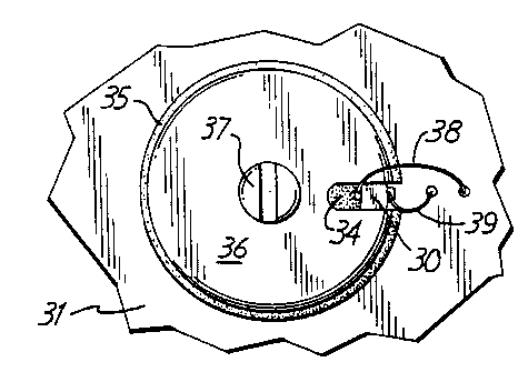
mechanical unbalances. A PZT ceramic ring, 30, is sh~t~
positioned in a recessed portion of a housing, 31, ~r~.th
the recessed portion being in the form of a flat b~ttom
hole in this housing thr~~ugh its upper surface; This
hole is enclosed by an outer vertical side surface
formed by h~using 31 having a circular cr~~s section,
there being a. central core, 32, in the hole ~n the fog
of a right cylinder about which the hole is forged
having an upper face substantially parallel to, and at
a height ab~ve, the upper surface of housing 31.
A 1~wer open cell, ~o~t foam material Dyer,
33, is prerv~:d~d on the exposed bottom surface of th~,s
hole with a central hole therein allowing cdr~ 32 t~
extend up there~through. Ceramic material ring 30 is
positioned thereover and around care 32, ring 30 being
kept approximately centered wzth respect to this core by
a furtheropen Cell, soft foam material layer, 34, in
they form of a round disk which is as thick as rung 30 is
high ~ ~ central hole in foam disk 34 permits core 3~ t~
also extend th~~~~hr~ugh.
17VU 93/14379 PGT/US93/007H7
-28--
An upper open cell, soft foam material layer,
35, is positioned over layer 3~ and much of the upper
surface of ring 30, arid around core 32 extending through
a hole therein. A clamping plate, 36, with a fastener
hole in the center, is positioned over much of ring 30
and layer 35, and all of core 32 except for the portion
of that core exposed by the fastener hole. A screw, 37,
goes through the fastener hole in clamping plate 3~ arid
into a tapped hole in core 32 centered in its upper
face.
Screw 37 is turned in until clamping plate 36
is forced tightly against the upper surface core 32~.
this action provides a fairly repeatable downward force
on the combination of ring-30: between open cell, soft
foam material layers 35 and 33 determined by the, height
of that r ng and the thickness of those layers egaven a
repeatable depth for the hole in hou$ing 31 arid a
repeatable height for core 32. Thus, the forces by
which ring 30 is held are reasonably well known from-
unit to unit and reasonably repeatebie
Layers 35 and 33 behave somewhat as nonlinear
springs in that ring 30 is rather lightly held by them
with very little s iffness in these layers in opposing
forces. of the ring applied to them if the ring is near
to being centered ~herebetween: However; the
oPPosi~ion of these layers to ring forces applied o
them increases very quickly if ri~ag 30 is forced a
significant distance in the direction of either of those
layers, as by mechanical shock, i.e: the layers become
relatively very stiff. Centering layer 34 behaves in a
s~.~ai~la~r manner if part of ring 3p is moved radially .
toward core-32.> This relatively light loading on ring
30 keeps. the generation of second harmonic motion
CA 02114149 2000-06-14
64159-1288
29
components during periodic motion of the ring forced by
generator 20 very small, but nevertheless leaves ring 30 well
restrained from relatively large motion excursions.
A pair of flexible wires, 38 and 39, are used to
electrically contact the inner and outer curved surfaces of
ring 30, respectively. Interconnection wires 38 and 39 are
very flexible and so provide a very small mechanical loading on
ring 30. A possible alternative to a ring, which would aid in
avoiding loading of interconnection wires 38 and 39, would be
to use a solid disk of ceramic material rather than a ring as
such disks under periodic motion develop stationary node
locations thereon at which such wires could be affixed to not
impede disk motion.
A portion, 40, of the optical fiber extending between
coupler 27 and coil 10, which is wrapped around ring 30 is
shown in Figures 2A and 2B to be wrapped around the central
portions of the curved outer surface of ring 30. Flexible wire
39 is connected to the curved outer surface of ring 30 above
the portion of that surface about which optical fiber portion
40 is wrapped. To substantially reduce hysteresis and slippage
in the stretching process undergone by the wrapped optical
fiber during modulation, the jacket on optical fiber portion
40, may be thin and hard, and should adhere well to the silica
core.
Also for this purpose, optical fiber portion 40 is
wrapped under tension of about 40 grams about the outer curved
surface of ring 30, and is done with that surface wet with
ultraviolet curable epoxy which suffuses through the wrapped
fiber portion and is thereafter cured to firmly bond that
portion to the outer curved surface of ring 30. Optical fiber
portion
CA 02114149 2000-06-14
64159-1288
-30-
40 is wrapped symmetrically about the outer surface of
ring 30 with an integral number of turns to avoid any
stretching of just a portion of a loop in that fiber
therearound.
Such a structure for phase modulator 19 can
result in a phase modulator in which the mechanical
response generated second harmonic component that
relatively easily achieves having mechanically induced
time varying second harmonic optical path phase changes
of amplitudes that are 80 dB less than the fundamental
frequency component amplitudes and, with care, will have
an amplitude more than 120 dB below that of the
fundamental component. Thus, the phase modulator of
Figures 2A and 2B can meet the requirement of providing
a second harmonic phase change component which is no
more than that permitted for the offset phase error
component in the output signal of the fiber optic
gyroscope system of Figure 1.
The expression found above for the offset
phase error due to the presence of second harmonic
components shows two further possibilities for reducing
or eliminating such an offset error. The first is found
in the factor [ 1-J3 ( Vim) /J1 ( apm) ~ which can be forced to
zero, or very close to zero, by choosing the amplitude
of the fundamental component of the phase change ~p~ at
a substantially higher value, 3.05, than the value used
to maximize the expected output signal, 1.84. This
would result in ~pR also becoming zero. A system for
selecting and maintaining amplitude values of the bias
modulation fundamental component is described in United
States Patent entitled "Fiber Optic Gyroscope Bias
Modulation Amplitude Determination" by P. Dane et al No.
CA 02114149 2000-06-14
64159-1288
-31-
5,196,904 and assigned to the same assignee as the
present application.
Although such an arrangement cannot keep
the bias modulation amplitude perfectly at 3.05, and
offsets due to larger quadrature signals increase, this
arrangement can be used to provide a relatively small
value for this factor, even if not zero, which can in
turn increase the limits which ~e and am must meet even
though the fiber optic gyroscope output signal offset
phase error specification remains unchanged.
The other remaining possibility for
eliminating or significantly reducing the offset phase
error shown in the equation found therefor is provided
by the factor cosc~gz/2. As is well known, there is a
so-called "proper frequency" for cog in operating phase
modulator 19 by modulation generator 20. At that
modulation frequency, the modulation of the counter-
propagating electromagnetic waves in coil 10 will be
180 ° out of phase which provides various benef it's in the
operation of a bias modulation system. The proper
frequency for ~9, or mg_p, is ~g_pr=n. At that
frequency, clearly wg/2=~r/2. Since cos~r/2=0, ~pR also
becomes zero. A phase modulator of the type described
in Figures 2A and 2B usually cannot operate at the
typical frequency this implies for relatively short
lengths of optical fiber being used to form coil 10
(although it is suitable for longer lengths) , and so one
option is to use an integrated optics chip phase
modulator particularly if a coiled loop fiber optic
gyroscope is involved.
If the typical value for ~m of 1.84 is again
used, rpm[ 1-J3 (rpm) /J1 (gym) 1 will be approximately one
again. On the other hand, the use of an integrated
wee ~~~ad~79 p~ius9~soo7a~
-3a-
~~'~
optics chip will eliminate help from the mechanical
response ratio, i.e. ~p2/cpl will be approximately one
since an integrated optics chip exhibits a wide
bandwidth in use of the electrooptic effect which
introduces no significant frequency dependent effects
wntil the capacitance between the electrodes becomes
significant at very.high frequencies. As a result, the
aid this factor brought in raising the limit to be met
by 6e is eliminated. Further, 8~ will be approximately
Zero so there will not be a mechanically induced second
harmonic component difficulty in using an integrated
optics chip of any significance, this result coming
about because the elasto~ptic effect in the material
body in such a chip is insignificant compared to the
electrooptic effect. Such ,integrated optics chips
exhibit other nonlinearities which result on~:y 3n
quadrature effects. In these circumstances, from the
result found fog i~R above, and again noting that sin~rg
must be considered a value of one, the error phase can
be written:
l~R~~ '°~ COS~~G59 2 ~b~
Howe~rer; there are substantial difficu~.ties in
attempting to set cosWg~/2 to Zero, or ~~/2 tn n/2,
because T is a function. ~f temperature due to the
p 25 eptical fiber in coil to expanding and contracting with
temperature changes. Typically; this temperature
depen3ence' is on the order of:
_1 _d~ ~ 1 p"~/° c
t dT
.. :: '.. ~.. . ~ .~. .; , ., ..... ," . ,... .. .,.. ,.~....;., ~ . '...
'.~",;S :.,~,~~',
WO 93/14379 PC'I'/US93/00717
33-
where T represents temperature on the Centrigade scale.
This temperature dependence leads to a corresponding
temperature dependence in cos~agT / 2 which f or r~gr / 2 being
approximately ~r/2 can be shown to be approximately:
dcos ~ t
dT ~° - 2 1.0'5/ c
Thus, for a maximum excursion of 60°~ from room
temperature, cos~gr/2 will change by as much as:
~COS~t~g1 ~~ ~ 60 2 10'S ~ 1Q'~
' Thus, ~ coswgz/2 ( cannot be expected to remain any closer
than within 10°3 of zero, and s~:
$e ~ ~°~
10_3
Hence, the req~uiremen~ on the relative
amplitude of the second harmonic component with xespect
to the first h~imonic component from modulati~n
generator 20 is less stx~in~~nt in the situation whieh
phase modulatar 19 is pperat~d at the proper frequency
by 60 d~. T'his can be achieved by use of an integrated
og~tic c~.rGUit rather than by a ceramic body having
optical fiber wrapped therearound or a long length ~f
optical fiber in coil 10 using such a ceramio body and
wra~a: ~n ' the other k~and; the expense of using an
integrated optie chip, or a long length ~f cail, or
b~th, often will mean that a high quality fiber ~ptic
gyroscope must be provided to mike it saleable at the
necessary price. Thue, ~~p~~max may be significantly
dc~~eased, such as ~o being less than 10"8, ~r only a
W(D 93/ 1 ~i379 FG f/US93/007 H 7
~l~
. ~-34-
fraction of a degree per hour. In the situation of an
integrated optics chip, the requirement on the amplitude
of the second harmonic component relative to the first
harmonic component provided by modulation generator 20,
8e, may be as stringent as it was in the previous
situation of ~ ~p~ ~ ~,ax being less than 10"5.
In many situations, modulation generator 20
will be desired for .convenience to provide a square wave
to operate phase modulator l9 rather than a sinusoid:
1.0 For instance; this waveform may be quite convenient in
certain demodulation schemes differing from the one
shown in the system of Figure 1: Such square waves, if
truly square, do not ~dntain even'harmonics, and so the
only harmonic likely to be significant, the second
harmonic, in operating phase modulator 19 would not be
present.
I~owever, providing a square wave to drive a
substantia3ly capacitive 1~ad may be,quite difficult,
particularly at higher frequencies. A duty cycle other
z~ than a 50% duty cycle i~ not a maj~r difficulty; as such
an asymmetrical rectangular wave merely raises the
quadrature signal pravided by the phase detector. ~n
the other hand, if the rise times and fall times of the
rectangular ware or the square wave are unequal, second
harmonic components will be generated leading to an
offset pha~a error: The limit on the r~sulting second
harmongc companent from generator ~0 xelative 'to the
f~xnd~mental component therefrom, 8~, would remain
related to the permitted fibeg optic gyroscope phase
3(H error lama as shown in the equati~ns therefor above,
and ~ge.n be shown to be related to rise and fall time
differences approximately as:
WO 93/ 143'79 PCT/US93/0~717
RISE ~'Il~?~E - FALL ?'IME
a
T
If coil 10 is chosen to be 1.0 km in length, T will be
approximately 5,us. If 6~ again must meet the
requirement de510°5, then the difference between the w
wave rise time and the fall time must not emceed .05 ns.
Although the present invention has been
described with reference to preferred embodiments,.
workers skilled in the art will recognize that changes
may be made in form and detail without departing fxo~
ZO the spirit and scope of the invention:
~,