Note: Descriptions are shown in the official language in which they were submitted.
21 l ~il 82
NARROW-BAND FILTER HAVING A VARIABLE CENTER FREQUENCY
Background of the Invention:
This invention relates to a narrow-band filter
having a variable center frequency. Such a narrow-band
filter is particularly useful for detecting a plurality
of tone signals which have different frequencies.
In general, a narrow-band filter comprises an
input terminal supplied with an input signal having a
predetermined frequency, an output terminal, first
through n-th low-pass filters which are connected in
parallel to one another, where n represents a first
positive integer greater than unity, a switching circuit
connected to the first through the n-th low-pass filters,
and a control circuit for controlling the switching
circuit. The first through the n-th low-pass filters
have the same filter characteristic and are collectively
called an n-path filter. The control circuit delivers
first through n-th switch driving signals to the
switching circuit. Supplied with the first through the
n-th switch driving signals, the switching circuit time
divisionally connects the first through the n-th low-pass
filters one by one between the input and the output
terminals at a predetermined period Tp. As a result of
switching operation of the switching circuit, the first
2 1 1 51 82
through the n-th low-pass filters time divisionally
filtering the input signal for first through n-th
filtering durations, respectively. The first through the
n-th filtering durations are equal to one another. In
this event, the narrow-band filter has a single center
frequency fc. Such a narrow-band filter is disclosed in
Japanese Unexamined Patent Prepublication No. 16013/1985
(Tokkai Shô 60-16013).
In the meantime, a mobile radio telephone system
of an AMPS type uses an SAT (Supervisory Audio Tone)
signal in order to monitor a connection state of a radio
channel. The SAT signal is carried by a radio signal and
has one of first through third tone frequencies which are
equal to 5970 (Hz), 6000 (Hz), and 6030 (Hz), respectively,
and which are assigned to base stations. Let the mobile
radio telephone system comprise first through third base
stations which are assigned with the first through the
third tone frequencies, respectively. When the first
base station transmits the SAT signal having the first
tone frequency, a mobile station receives the SAT signal
transmitted from the first base station. When the mobile
station detects the first tone frequency of the SAT signal,
the mobile station transmits a transmission signal, as an
answer back signal, having a frequency equal to the first
tone frequency. On reception of the transmission signal
having the frequency equal to the first tone frequency,
the first base station confirms the fact that the radio
channel is connected to the mobile station.
21 1 51 82
As apparent from the above description, the
mobile station must discriminate a tone frequency among
the first through the third tone frequencies. The
narrow-band filter mentioned above is particularly useful
for detecting the tone frequency. However, the mobile
station must be provided with first through third narrow-
band filters having first through third center frequencies
which are equal to the first through the third tone
frequencies, respectively. This is because the narrow-
band filter detects a single tone frequency only. Thismeans that the mobile station requires a receiver circuit
of a large size for discriminating the tone frequency
among the first through the third tone frequencies.
Sum~ary of~the Invention:
It is therefore an object of this invention to
provide a narrow-band filter which is capable of changing
a center frequency in a narrow range.
It is another object of this invention to provide
a narrow-band filter of the type described without
increment of a circuit size.
Other object of this invention will become clear
as the description proceeds.
On describing the gist of this invention, it is
possible to understand that a narrow-band filter is
supplied with an input signal having a predetermined
frequency through an input terminal. The narrow-band
filter filters the input signal and produces a filtered
signal through an output terminal. The narrow-band
21 1 51 82
filter comprises first through n-th low-pass filters
which are connected in parallel to one another, where n
represents a positive integer greater than unity, and
switching means connected to the first through the n-th
low-pass filters for time divisionally connecting the
first through the n-th low-pass filters between the input
and the output terminals. The first through the n-th
low-pass filters time divisionally filters the input
signal for first through n-th filtering durations,
respectively, and produces first through n-th time
division filtered signals, respectively, collectively as
the filtered signal. The narrow-band filter further
comprises control means connected to the switching means
and supplied with a frequency designation signal
designating the predetermined frequency for controlling
the switching means to change at least one of the first
through the n-th filtering durations in accordance with
the frequency designation signal.
Brief Description of the Drawing:
Fig. 1 is a block diagram of a conventional
narrow-band filter;
Fig. 2 shows signal waveforms for use in
describing operation of the narrow-band filter
illustrated in Fig. l;
Fig. 3 is a block diagram of a narrow-band filter
according to a preferred embodiment of this invention;
Fig. 4 shows an example of a circuit arrangement
in a signal generating circuit illustrated in Fig. 3;
21 15182
Fig. 5 shows a circuit arrangement of a variable
frequency divider illustrated in Fig. 3;
Fig. 6 shows signal waveforms for use in
describing first operation of the variable frequency
divider illustrated in Fig. 5;
Fig. 7 shows signal waveforms for use in
describing second operation of the variable frequency
divider illustrated in Fig. 5;
Fig. 8 shows signal waveforms for use in
describing operation of the narrow-band filter
illustrated in Fig. 3;
Fig. 9 shows signal waveforms for use in
describing third operation of the variable frequency
divider illustrated in Fig. 5; and
Fig. 10 shows signal waveforms for use in
describing another operation of the narrow-band filter
illustrated in Fig. 3.
Description of the Preferred Embodiment:
Referring to Figs. 1 and 2, a conventional
narrow-band filter will be described at first in order
to facilitate an understanding of the present invention.
In Fig. 1, the narrow-band filter comprises a filter
circuit 10 which is called an n-pass filter and a control
circuit 20. The filter circuit 10 is for filtering an
input signal having a predetermined frequency fi and
produces a filtered signal. The filter circuit 10
comprises an input terminal 11 supplied with the input
signal, an output terminal 12, and first through n-th
6 211~182
low-pass filters 13-1 to 13-n which are connected in
parallel to one another, where n represents a first
positive integer greater than unity. The first through
the n-th low-pass filters 13-1 to 13-n have the same
filter characteristic, for example, the same cutoff
frequency of 3 dB.
The filter circuit 10 further comprises first
through n-th input switches 14-1 to 14-n which are
connected between the input terminal 11 and the first
through the n-th low-pass filters 13-1 to 13-n and first
through n-th output switches 15-1 to 15-n which are
connected between the output terminal 12 and the first
through the n-th low-pass filters 13-1 to 13-n. The
first through the n-th input switches 14-1 to 14-n and
the first through the n-th output switches 15-1 to 15-n
may collectively be called a switching circuit.
As will later be described, the switching circuit
is controlled by the control circuit 20 and time
divisionally connects the first through the n-th low-pass
filters 13-1 to 13-n one by one between the input and the
output terminals 11 and 12.
The control circuit 20 comprises an oscillator
21, a frequency divider 22 connected to the oscillator
21, and a ring counter 23 connected to the frequency
divider 22. The oscillator 21 generates a reference
clock signal having a reference frequency fO. The
frequency divider 22 frequency divides the reference
clock signal by a predetermined frequency dividing ratio
7 21 15182
l/m where m represents a second positive integer greater
than unity. The frequency divider 22 delivers a divided
clock signal CK having a divided frequency fr given by
fO/m to the ring counter 23. The divided clock signal CK
is illustrated at a top line of Fig. 2. Supplied with
the divided clock signal CK, the ring counter 23 counts
the number of clocks of the divided clock signal CK and
time divisionally generates first through n-th count
signals in the manner known in the art. The ring counter
23 supplies the first through the n-th count signals, as
first through n-th switch driving signals Sl to Sn, to
the first through the n-th input switches 14-1 to 14-n,
respectively, and to the first through the n-th output
switches 15-1 to 15-n, respectively.
In Fig. 2, the first through a tenth switch
driving signals Sl to S10 are illustrated on the
supposition that first integer n is equal to 10. The
first through the tenth switch driving signals Sl to S10
have the same driving frequency fp and have first through
tenth high level durations, respectively, defined by a
high level, namely, a logic one value. Each of the first
through the tenth high level durations lasts a constant
time duration Td and which repeats at a predetermined
period Tp. It should be noted here that the first
through the tenth high level durations never overlap on a
time base. In other words, the first through the tenth
switch driving signals Sl to S10 have first through tenth
phases which are different from one another.
21 1 51 82
Turning back to Fig. 1, the first through the
n-th input switches 14-1 to 14-n are put into an on state
by the first through the n-th switch driving signals Sl
to Sn, respectively. The first through the n-th output
switches 15-1 to 15-n are also put into an on state by
the first through the n-th switch driving signals Sl to
Sn, respectively. For example, the first input and the
first output switches 14-1 and 15-1 are put into the on
state at the same time by the first switch driving signal
Sl. As a result, the first low-pass filter 13-1 is
connected between the input and the output terminals 11
and 12 in a time period during which the first input and
the first output switches 14-1 and 15-1 are put into the
on state. In other words, the first low-pass filter 13-1
filters the input signal for a first filtering duration
which corresponds to the first high level duration and
which is equal to the constant time duration Td. The
first low-pass filter 13-1 delivers a first time division
filtered signal to the output terminal 12.
Next, the second input and the second output
switches 14-2 and 15-2 are put into the on state at the
same time by the second switch driving signal S2. The
second low-pass filter 13-2 is connected between the
input and the output terminals 11 and 12 in a time period
during which the second input and the second output
switches 14-2 and 15-2 are put into the on state. Thus,
the second low-pass filter 13-2 filters the input signal
for a second filtering duration which corresponds to the
21 1 51 82
second high level duration and which is equal to the
constant time duration Td. The second low-pass filter
13-2 delivers a second time division filtered signal to
the output terminal 12.
Similarly, the third through the n-th low-pass
filters 13-3 to 13-n filter the input signal, in order,
for third through n-th filtering durations which are
equal to the constant time duration Td. It should be
noted here that the first through the n-th filtering
durations are equal to the constant time duration Td and
never overlap on the time base. This means that the
first through the n-th low-pass filters 13-1 to 13-n time
divisionally filter the input signal and produce the
first through the n-th time division filtered signals,
respectively, collectively as the filtered signal. In
the manner mentioned above, the narrow-band filter has a
narrow-band filter characteristic defined by a center
frequency fc. The narrow-band filter is, in general,
called a narrow-band n-path filter.
In the narrow-band filter being illustrated, the
center frequency fc is equal to the driving frequency fp
of the first through the n-th switch driving signals Sl
to Sn. Furthermore, a band width of 3 dB of the
narrow-band filter is equal to twice the cutoff frequency
of 3 dB of the first through the n-th low-pass filters
13-1 to 13-n. On the other hand, the driving frequency
fp is related to the divided frequency fr mentioned in
conjunction with the frequency divider 22 and is defined
21 1 51 82
by a first equation given by:
fp (= fc) = fr/n. (1)
As mentioned in conjunction with the frequency divider
22, the divided frequency fr is defined by a second
equation given by:
fr = fO/m. (2)
From the first and the second equations (1) and
(2), the center frequency fc is defined by a third
equation given by:
fc = fr/n = fO/(m x n). (3)
In addition, it is desirable that the first positive
integer n is equal to ten at most in order to minimize
the size of the narrow-band filter.
Taking the above into consideration, if the
oscillator 21 is implemented by a crystal oscillator, the
reference clock signal has a precise frequency equal to
the reference frequency fO. As a result, the center
frequency fc can be set at a correct value. Furthermore,
if the cutoff frequency of 3 dB of the first through the
n-th low-pass filters 13-1 to 13-n is set at a low value,
it is possible to narrow the band width of 3 dB of the
narrow-band filter. This means that the narrow-band
filter is particularly useful for detecting the input
signal having the predetermined frequency equal to the
center frequency fc. Under the circumstances, the
narrow-band filter comprising the n-path filter is used
for detecting a tone signal.
11 2 1 1 5 1 82
In the meantime, a mobile radio telephone system
of an AMPS type uses an SAT (Supervisory Audio Tone)
signal in order to monitor a connection state of a radio
channel. The SAT signal is carried by a radio signal and
has one of first through third tone frequencies which are
equal to 5970 (Hz), 6000 (Hz), and 6030 (Hz), respectively.
A frequency difference between the first and the second
tone frequencies is an extremely small value which is
equal to 30 (Hz) and is 0.5 (%) relative to the second
tone frequency. This applies to the frequency difference
between the second and the third tone frequencies. The
first through the third tone frequencies are assigned to
base stations which have different radio communication
areas. Let the mobile radio telephone system comprise
first through third base stations which have first through
third radio communication areas and which use the first
through the third tone frequencies, respectively. If the
first base station transmits the SAT signal having the
first tone frequency, a mobile station located in the
first radio communication area receives the SAT signal
transmitted from the first base station. When the mobile
station detects the first tone frequency of the SAT signal,
the mobile station transmits a transmission signal, as an
answer back signal, having a frequency equal to the first
tone frequency. On reception of the transmission signal
having the frequency equal to the first tone frequency,
the first base station confirms the fact that the radio
channel is connected to the mobile station.
12 2 1 1 5 1 82
As apparent from the above description, the
mobile station must discriminate a tone frequency among
the first through the third tone frequencies. The
narrow-band filter mentioned above is used in a receiver
circuit of the mobile station for detecting a
predetermined one of the first through the third tone
frequencies. In order to discriminate the tone frequency
among the first through the third tone frequencies, the
mobile station must be provided with first through third
narrow-band filters having first through third center
frequencies which are equal to the first through the
third tone frequencies, respectively. This means that
the mobile station requires the receiver circuit which is
expensive and which has a large size in order to
discriminate the tone frequency among the first through
the third tone frequencies.
In order to dissolve the above-mentioned
disadvantage, it will be supposed to time divisionally
detect the first through the third tone frequencies by
changing the center frequency fc. In order to change the
center frequency fc, the following methods will be
considered taking the third equation (3) mentioned before
into consideration.
In a first method, the reference frequency fO is
changed. In a second method, the first positive integer
n is changed. In a third method, the second positive
integer m is changed. In the first method, it is
required to use an oscillator of a variable frequency
2 1 1 5 1 82
type. This means that it is impossible to use the
crystal oscillator having a high accuracy. As a result,
the reference frequency becomes unstable. In order to
stabilize the reference frequency, it will be considered
that the oscillator is combined with a PLL (Phase Lock
Loop) circuit. In this case, the narrow-band filter
requires a complex analog circuit for the PLL circuit.
In the second method, it is hard to change the
center frequency by 0.5 (%), namely, 30 (Hz), even if the
first positive integer n is changed. This is because the
first positive integer n is equal to ten at most as
mentioned in conjunction with the equation (3). In the
third method, it is required that the second positive
integer m is greater than 200 in order to change the
center frequency by 0.5 (%). If the center frequency fc,
the first positive integer n, and the second positive
integer m are equal to 6000 (Hz), 10, and 200,
respectively, the reference frequency fO becomes an
extremely high frequency which is equal to 12 (MHz). In
this event, the frequency divider 22 must operate in high
speed. This means that the frequency divider 22 requires
a high power consumption.
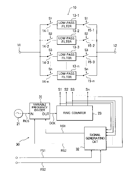
Referring to Fig. 3, the description will proceed
to a narrow-band filter, namely, a narrow-band n-path
filter, according to a preferred embodiment of this
invention. The narrow-band filter is particularly useful
for detecting three kinds of tone signals which have the
first through the third tone frequencies and is therefore
14 2 1 1 5 1 82
included in the receiver circuit of the mobile station.
The narrow-band filter comprises similar parts designated
by like reference numerals and a control circuit 30 used
in place of the control circuit 20. The control circuit
30 comprises similar parts designated by like reference
numerals, a variable frequency divider 31 which is used
in place of the frequency divider 22, and additionally a
signal generating circuit 32. As will later be
described, the variable frequency divider 31 frequency
divides the reference clock signal by one of first
through third frequency dividing ratios of l/~m-l), l/m,
and l/(m+l). The first through the third frequency
dividing ratios are determined by first and second ratio
designation signals RSl and RS2 supplied from the signal
generating circuit 32.
The signal generating circuit 32 is supplied with
the first through the n-th switch driving signals Sl to
Sn from the ring counter 23 and supplied with first and
second frequency designation signals FSl and FS2 from a
micro processor (not shown). As well known in the art,
the micro processor controls a transmitter and a receiver
in the mobile station. In the example, the micro
processor produces the first and the second frequency
designation signals FSl and FS2 in order to designate the
frequency dividing ratio. Although the signal generating
circuit 32 is supplied with the first through the n-th
switch driving signals Sl to Sn, the signal generating
circuit 32 utilizes only one of the first through the
21 1 51 82
n-th switch driving signals Sl to Sn as will become clear
as the description proceeds. As will shortly be
described, the signal generating circuit 32 produces the
first and the second ratio designation signals RSl and
RS2 in accordance with the first and the second frequency
designation signals FSl and FS2 and one of the first
through the n-th switch driving signals Sl to Sn. Such a
signal generating circuit 32 can be implemented by a
decoder known in the art. The first and the second
frequency designation signals FSl and FS2 may
collectively be called a frequency designation signal.
Similarly, the first and the second ratio designation
signals RSl and RS2 may collectively be called a ratio
designation signal.
Practically, the micro processor produces the
first and the second frequency designation signals FSl
and FS2 so as to designate periodically the first through
the third frequency dividing ratios of l/(m-l), l/m, and
l/(m+l) one after another at a prescribed period. For
example, the micro processor designates at first the
first frequency dividing ratio of l/(m-l) during a first
time duration. Next, the micro processor designates the
second frequency dividing ratio of l/m during a second
time duration succeeding the first time duration.
Subsequently, the micro processor designates the third
frequency dividing ratio of l/(m+l) during a third time
duration succeeding the second time duration. The micro
processor repeats the above mentioned designation
16
operation at the prescribed period. 2 1 1 5 1 82
Let the signal generating circuit 32 utilize a
sixth switch driving signal S6. In this event, the
signal generating circuit 32 is realized by first and
second AND gates 32-1 and 32-2 as shown in Fig. 4. In
Fig. 4, the first AND gate 32-1 is supplied with the
sixth switch driving signal S6 and the first frequency
designation signal FSl while the second AND gate 32-2 is
supplied with the sixth switch driving signal S6 and the
second frequency designation signal FS2. The first AND
gate 32-1 produces the first ratio designation signal RSl
having the logic one value only when both the sixth
switch driving signal S6 and the first frequency
designation signal FSl have the logic one value. At this
time, the second AND gate 32-2 produces the second ratio
designation signal RS2 having the logic zero value. On
the other hand, the second AND gate 32-2 produces the
second ratio designation signal RS2 having the logic one
value only when both the sixth switch driving signal S6
and the second frequency designation signal RS2 have the
logic one value. At this time, the first AND gate 32-1
produces the first ratio designation signal RSl having
the logic zero value.
Turning back to Fig. 3, the variable frequency
divider 31 selects one of the first through the third
frequency dividing ratios of l/(m-l), l/m, and l/(m+l) in
accordance with the first and the second ratio
designation signals RSl and RS2. In the example being
21 1 5 1 82
illustrated, the variable frequency divider 31 selects
the second frequency dividing ratio of l/m when both the
first and the second ratio designation signals RSl and
RS2 have the logic zero value. The variable frequency
divider 31 selects the first frequency dividing ratio of
l/(m-l) when the first ratio designation signal RSl has
the logic zero value and when the second ratio set signal
RS2 has the logic one value. The variable frequency
divider 31 selects the third frequency dividing ratio of
l/(m+l) when the first ratio designation signal RSl has
the logic one value and when the second ratio designation
signal RS2 has the logic zero value.
The description will be directed to the case
where the reference frequency f0, the first positive
integer n, and the second positive integer m are equal to
1200 (kHz), 10, and 20, respectively. In this case, the
variable frequency divider 31 implemented by a circuit
illustrated in Fig. 5. In Fig. 5, the variable frequency
divider 31 comprises first through fifth D-type flip-flop
circuits 51 to 55 which are connected in series, sixth
and seventh flip-flop circuits 56 and 57, AND gates 58 to
63, an OR gate 64, and an NAND gate 65.
Referring to Fig. 6 together with Figs. 3 to 5,
let the variable frequency divider 31 receive the first
and the second ratio designation signals RSl and RS2 have
the logic zero value. The first D-type flip-flop circuit
51 is supplied from the oscillator 21 implemented by the
crystal oscillator with the reference clock signal. The
18 21 1 51 82
reference clock signal is depicted at RCS and illustrated
at a top line of Fig. 6. In this event, the first D-type
flip-flop circuit 51 produces a first divided signal Ql
wherein the reference clock signal RCS is divided by the
frequency dividing ratio of 1/2. The first divided
signal Ql is shown at a second line of Fig. 6. The
second D-type flip-flop circuit 52 produces a second
divided signal Q2 wherein the reference clock signal RCS
is divided by the frequency dividing ratio of 1/4. The
second divided signal Q2 is shown at a third line of Fig.
6. Similarly, the third D-type flip-flop circuit 53
produces a third divided signal Q3 which is divided by
the frequency dividing ratio of 1/8. The fourth D-type
flip-flop circuit 54 produces a fourth divided signal Q4
(shown at a fourth line of Fig. 6) which is divided by
the frequency dividing ratio of 1/16. On the other hand,
the fifth D-type flip-flop circuit 55 is reset by reset
operation before the fifth D-type flip-flop circuit 55
completes frequency dividing operation by the frequency
dividing ratio of 1/32. In other words, the fifth D-type
flip-flop circuit 55 produces a fifth divided signal Q5
(shown at a sixth line of Fig. 6) in the middle of the
frequency dividing operation by the frequency dividing
ratio of 1/32 for the following reason.
Namely, the NAND gate 65 produces a gate output
signal S65 having the logic zero value at a twentieth
clock of the reference clock signal RCS from start of
frequency dividing operation. A start time of the
19 21 1 51 82
frequency dividing operation is depicted at Ts in Fig. 6.
By the gate output signal S65 having the logic zero
value, the first through the fifth D-type flip-flop
circuits 51 to 55 are reset at the same time. As a
result of reset operation, the fifth D-type flip-flop
circuit 55 produces a divided clock signal DCK through an
inverter terminal Q. It should be noted here that the
divided clock signal DCK is an inverted signal wherein
the fifth divided signal Q5 is inverted in polarity.
Moreover, the divided clock signal DCK is a signal
wherein the reference clock signal RCS is divided by the
frequency dividing ratio of 1/20. Supplied with the
divided clock signal DCK defined by the frequency
dividing ratio of 1/20, the ring counter 23 delivers the
first through the tenth switch driving signals Sl to S10
which are similar to that illustrated in Fig. 2.
Supplied with the first through the tenth switch driving
signals Sl to S10, the filter circuit 10 carries out the
same filtering operation similar to that described in
conjunction with Fig. 1. As a result of the above
operation, the narrow-band filter has the center
frequency which is equal to 6000 (= 1200 x 103/(20 x 10))
(Hz). The narrow-band filter can detect the input signal
having the predetermined frequency equal to the center
frequency. In other words, the narrow-band filter serves
as a detector for detecting the input signal, such as a
tone signal, having the second tone frequency, as the
predetermined frequency, equal to 6000 (Hz).
21 1 51 82
Referring to Figs. 7 and 8 together with Figs. 3
to 5, let the micro processor produce the first frequency
designation signal FSl having the logic one value and the
second frequency designation signal FS2 having the logic
zero value. In this event, the signal generating circuit
32 delivers the first ratio designation signal RSl having
the logic one value and the second ratio designation
signal RS2 having the logic zero value. In other words,
the first ratio designation signal RSl has the logic one
value in a time period during which the sixth switch
driving signal S6 has the logic one value as apparent
from Fig. 4. Furthermore, the sixth low-pass filter 13-6
carries out the filtering operation in a time period
during which the sixth switch driving signal S6 has the
logic one value. On the other hand, the variable
frequency divider 31 selects the third frequency dividing
ratio of l/(m+l), namely, 1/21, in a time period during
which the sixth low-pass filter 13-6 carries out the
filtering operation. This means that the variable
frequency divider 31 carries out the frequency dividing
operation by the third frequency dividing ratio of 1/21
in a time period during which the sixth low-pass filter
13-6 carries out the filtering operation.
In Fig. 5, the NAND gate 65 produces the gate
output signal S65 having the logic zero value at a
twenty-first clock of the reference clock signal RCS from
the start of the frequency dividing operation. By the
gate output signal S65 having the logic zero value, the
first through the fifth D-type flip-flop circuits are 5 82
reset at the same time. As a result of the reset
operation, the fifth D-type flip-flop circuit 55 produces
the divided clock signal DCK through the inverter
5 terminal Q. The divided clock signal DCK is the signal
wherein the reference clock signal RCS is divided by the
frequency dividing ratio of 1/21 in a time period during
which the sixth low-pass filter 13-6 carries out the
filtering operation. This means that the sixth filtering
10 duration of the sixth low-pass filter 13-6 is extended
for one cycle duration of the reference clock signal RCS.
In other words, the sixth filtering duration becomes
longer by one cycle duration than the first through the
fifth filtering durations and the seventh through the
15 tenth filtering durations which are depicted at Td in
Fig. 8. Such an extended sixth filtering duration is
depicted at Td21 in Fig. 8. Although the sixth high
level duration is extended, the first through the tenth
high level durations never overlap one another. As a
20 result of the above operation, the narrow-band filter has
the center frequency which is approximately equal to 5970
(= 1200 x 10 /(20 x 10 + 1)) (Hz). In this case, the
narrow-band filter serves as the detector for detecting
the tone signal having the first tone frequency equal to
5970 (Hz).
Referring to Figs. 9 and 10 together with Figs. 3
to 5, let the micro processor produce the first frequency
designation signal FSl having the logic zero value and
22 21 15182
the second frequency designation signal FS2 having the
logic one value. In the case, the signal generating
circuit 32 delivers the first ratio designatlon signal
RSl having the logic zero value and the second ratio
designation signal RS2 having the logic one value. In
other words, the second ratio designation signal RS2 has
the logic one value in a time period during which the
sixth switch driving signal S6 has the logic one value.
The sixth low-pass filter 13-6 carries out the filtering
operation in a time period during which the sixth switch
driving signal S6 has the logic one value. On the other
hand, the variable frequency divider 31 selects the first
frequency dividing ratio of l/(m-l), namely, 1/19, in a
time period during which the sixth low-pass filter 13-6
carries out the filtering operation. This means that the
variable frequency divider 31 carries out the frequency
dividing operation by the first frequency dividing ratio
of 1/19 in a time period during which the sixth low-pass
filter 13-6 carries out the filtering operation.
In Fig. 5, the NAND gate 65 produces the gate
output signal S65 having the logic zero value at a
nineteenth clock of the reference clock signal RCS from
the start of the frequency dividing operation. The first
through the fifth D-type flip-flop circuits 51 to 55 are
reset at the same time by the gate output signal S65
having the logic zero value. As a result of the reset
operation, the fifth D-type flip-flop circuit 55 produces
the divided clock signal DCK through the inverter
23 21 1 51 82
terminal Q. The divided clock signal DCK is the signal
wherein the reference clock signal RCS is divided by the
frequency dividing ratio of 1/19 in a time period during
which the sixth low-pass filter 13-6 carries out the
filtering operation. This means that the sixth filtering
duration of the sixth low-pass filter 13-6 is shortened
by one cycle duration of the reference clock signal RCS.
In other words, the sixth filtering duration becomes
shorter by one cycle duration than the first through the
fifth filtering durations and the seventh through the
tenth filtering durations which are depicted at Td in
Fig. 10. Such a shortened sixth filtering duration is
depicted at Tdl9 in Fig. 10. Although the sixth high
level duration is shortened, the first through the tenth
high level durations never overlap one another. As a
result of the above operation, the narrow-band filter has
the center frequency which is approximately equal to 6030
(= 1200 x 10 /(20 x 10 - 1) (Hz). In this case, the
narrow-band filter serves as the detector for detecting
the tone signal having the third tone frequency equal to
6030 (Hz).
As apparent from the above description, the
narrow-band filter according to this invention can change
the center frequency in a narrow range without a complex
PLL circuit and a frequency divider which operates in
high speed. The narrow-band filter can detect all the
first through the third tone frequencies of the tone
signal. The narrow-band filter is therefore useful for
24 21 1~182
detecting a plurality of tone signals, such as SAT
signals which are used for the mobile radio telephone
system of the AMPS type and which have extremely small
frequency differences.
While this invention has thus far been described
in conjunction with a preferred embodiment thereof, it
will readily be possible for those skilled in the art to
put this invention into practice in various other
manners. For example, the variable frequency divider may
have four or more kinds of frequency dividing ratios.
The signal generating circuit may be implemented by
another circuit different from the circuit illustrated in
Fig. 4 and may select a plurality of switch driving
signals from the first through the N-th switch driving
signals. In this event, if the first and the second
switch driving signals are selected, the first and the
second filtering durations are changed.