Note: Descriptions are shown in the official language in which they were submitted.
21l5814
TITLE OF THE INVENTION
VOLTAGE-TYPE SELF-COMMUTATED CONVERSION SYSTEM
BACKGROUND OF THE INVENTION
Field of the Invention
This invention relates to a power conversion system,
and more particularly to a voltage-type self-commutated
conversion system such as a self-commutated reactive power
compensator device which performs voltage control, reactive
power control and so forth of power system and a self-
commutated power conversion system which performs power
interchange by means of DC transmission and frequency
conversion.
Description of the Related Art
Figure 4, a diagram for the purpose of explaining the
prior art, shows a voltage-type self-commutated power
converter 1 (referred to simply as a converter below) which
connects to an AC system 4 via a 3-phase system connection
transformer 3, together with its-control devices. 2is a DC
capacitor, 8, 9 and 10 are current transformers tCTs), 11 is
a converter output voltage reference computation circuit, 12
-- 1 --
;
2115S14
is a synchronization detection circuit, 13 is an active
current setting device, 14 is a reactive current setting
device, 15 is a PWM gate control circuit and 20 is a
protection circuit for the converter 1.
In Figure 4, the converter 1 is composed of self-turn-
off devices GU, GV, GW, GX, GY and GZ, for example GTOs
(gate turn-off thyristors), power transistors, static
induction thyristors and other power electronic devices with
self-turn off function, together with diodes, DU, DV, DW,
DX, DY and DZ connected respectively in anti-parallel with
each self-turn-off device.
Hereinafter, explanation will be given in the case
where the converter 1 is operated as an inverter for
converting DC input power into AC output power. The 3-phase
output voltage of the converter 1 in a system with this kind
of construction can be controlled by varying the conducting
period of the self-turn-off devices, GU, GV, GW, GX, GY and
GZ. The current received from or delivered to the AC system
4 via the impedance of the system connection transformer 3
is controlled by adJusting the phase angle and amplitude of
the 3-phase output voltage of the converter 1 in accordance
with the phase angle and amplitude of the system voltage VR,
VS and VT of the AC system 4. By this means, the voltage-
type self-commutated conversion system composed of the
converter 1, the DC capacitor 2 and the system connection
transformer 3 can either exchange active power with the AC
2~ 81~
-
system 4 by converting DC power to active power or
compensate the reactive power of the AC system 4.
The converter output voltage reference computation
circuit 11, the synchronization detection circuit 12, the
active current setting device 13, the reactive current
setting device 14 and the PWM gate control circuit 15
constitute a control device for the voltage-type self-
commutated conversion system which controls the active power
and reactive power.
The synchronization detection circuit 12 detects the
system voltage phase angle ~ of the system voltages VR, VS
and VT of the 3-phase AC system 4. The converter output
voltage reference computation circuit 11 computes converter
output voltage references VRc, VSc and VTc which determine
the output voltage of the 3 phases of the converter 1 in
order to regulate the converter output AC currents iR, iS
and iT detected by the current transformers 8, 9 and 10 in
accordance with an active current reference iqc from the
active current setting device 13 and a reactive current
reference idc from the reactive current setting device 14.
The converter output voltage reference computation
circuit 11 determines the phase angles of the convertér
output voltage references VRc, VSc and VTc to the system
voltages VR, VS and VT based on the system voltage phase
angle ~ detected by the synchronization detection circuit
12.
21I581~
~- The PWM gate control circuit 15 outputs gate singals
U1, V1, W1, X1, Y1 and Z1 which determine the conducting
periods of the sel~-turn-off devices GU, GV, GW, GX, GY and
GZ of the converter 1 by comparing the converter output
voltage references VRc, VSc and VTc with a triangular wave
carrier signal generated based on the system voltage phase
angle ~.
A protection signal P1 is generated from a protective
relay element (not shown) in order to protect the converter
1 from overcurrent, overvoltage and so forth.
The construction of the protection circuit 20 will be
described with reference to Figure 5. The gate signals U1,
V1, W1, X1, Y1 and Z1 from the PWM gate control circuit 15
are applied to first input terminals of AND circuits 20U,
20V, 20W, 20X, 20Y and 20Z, respectively. The protection
signal P1 is applied to second input terminals of the AND
circuits 20U, 20V, 20W, 20X, 20Y and 20Z through an inverter
circuit 20I. The AND circuits 20U, 20V, 20W, 20X, 20Y and
20Z generates gate signals Ug, Vg, Wg, Xg, Yg and Zg, which
are applied to gates of the self-turn-off devices GU, GV,
GW, GX, GY and GZ of the converter 1, respectively.
When the protection signal pl is not present, the
protection circuit 20 generates the gate signals U1, V1, W1,
X1, Y1 and Z1 as the gate signals Ug, Vg, Wg, Xg, Yg and Zg
to the converter 1 to control the conducting periods of the
self-turn-off devices GU, GV, GW, GX, GY and GZ,
- 4 -
~1~5814
respectively. When the protection signal P1 is generated,
the protection circuit 20 stops the gate signals U1, Vl, W1,
X1, Y1 and Z1 of the PWM gate control circuit 15 and
generates gate signals Ug, Vg, Wg, Xg, Yg and Zg to turn off
all the self-turn-off devices GU, GV, GW, GX, GY and GZ in
order to protect the converter 1 from overcurrent,
overvoltage and so forth in accordance with the protection
signal P1 from a protective relay element not shown in the
diagram.
The conventional voltage-type self-commutated
conversion system shown in Figure 4 suffers from the types
of problems described below. Because the output voltage of
the converter 1 and the AC voltage diverge if the AC voltage
is distorted owing to the introduction of the power
capacitor or the transformer and so forth, which are
connected to the AC system 4 and not shown in the diagram,
the output AC current of the converter 1 can increase and
become an overcurrent. When this happens, the overcurrent
relay not shown in the diagram operates and the self-turn-
off device GU, GV, GW, GX, GY and GZ are all turned off by
the protection circuit 20.
Figure 6 shows the state of the converter 1 immediately
before this. The dashed lines in Figure 6 show the flow of
current immediately before the protective action; for
example, R-phase current is flowing in-towards the +
(positive) side DC bus line P of the converter I from the AC
2II58I~
-
system 4 through the diode DU. The self-turn-off device GV
has been turned on by PWM control, and S-phase current
returns to the AC system 4 through the self-turn-off device
GV. T-phase current returns to the AC system 4 from the DC
capacitor 2 through the - (negativè) side DC bus line N and
the diode DZ.
If the R-phase current becomes an overcurrent in the
situation of Figure 6, the self-turn-off devices GU, GV, GW,
GX, GY and GZ are all turned off by the action of the
protection circuit 20 of Figure 4. When this happens, S-
phase current becomes unable to flow through the self-turn-
off device GV and returns to the AC system 4 via the +
(positive) side DC bus line P, the DC capacitor 2 and the
diode DY. This flow of current is shown by a solid line.
The flow of current shown by the solid line in Figure 6
is in the direction which charges up the DC capacitor 2.
Since this charging current is a large one, sufficient for
the overcurrent relay not shown in the diagram to operate,
the DC voltage rises to some extent. Because of this, a DC
overvoltage is generated and there is a risk of damage to
the converter 1 or devices connected to the DC bus lines P
and N.
With a conventional control and protection system,
there is therefore, contrary to what is intended, a risk of
- generating a DC overvoltage as a result of the protective
action of the converter. Th2 withstand capability to
21 I 581`-q
-
overvoltage of a semiconductor device is inherently less
than that to overcurrent, and it becomes damaged if the
overvoltage exceeds its withstand capability even
instantaneously. There is therefore a considerable risk of
damaging the converter by the protective action instead of
protecting it. There is consequently a danger of being
unable to restart a voltage-type self-commutated conversion
system after a voltage waveform distortion has abated, and
the system's essential purpose, voltage control and reactive
power control of power system or a power interchange,
becomes impossible.
SUMMARY OF THE INVENTION
Accordingly, one object of this invention is to provide
a voltage-type self-commutated conversion system which can
in safety protectively shut down a voltage-type self-
commutated power converter without raising the DC voltage.
These and other objects of this-invention can be
achieved by providing a voltage-type self-commutated
conversion system including a voltage-type self-commutated
power converter with a plurality of anti-parallel circuits
of a self-turn-off device and a diode. DC terminals of the
power converter are connected to DC bus lines of the voltage-
type self-commutated conversion system. The voltage-type
2115814
self-commutated conversion system further includes a DC
capacitor connected between the DC bus lines, a transformer
connected between an AC system and AC terminals of the power
converter and a control circuit for controlling the power
converter. The control circuit includes a gate control
circuit for generating gate signals for determining
conduction periods of the self-turn-off devices in the power
converter, a first protection circuit for turning on the
self-turn-off devices connected to positive side of the DC
bus lines in case of protective shutdown of the power
converter and a second protection circuit for turning off
the self-turn-off devices connected to negative side of the
DC bus lines in case of the protective shutdown of the power
converter.
According to the invention, the self-turn-off devices
connected to the + (positive) side DC bus line of the
converter are turned on in accordance with a protection
signal from the protection circuit. Contrarily, the self-
turn-off devices connected to the - (negative) side DC bus
line are turned off. As a result of this, no current flows
into the DC capacitor, and the current returns to the AC
system through one or other of thè turned-on self-turn-off
devices. The DC capacitor is thus not charged up, and the
DC voltage does not rise.
21~.~814
BRIEF DESCRIPTION OF THE DRAWINGS
A more complete appreciation of the invention and many
of the attendant advantages thereof will be readily obtained
as the same becomes better understood by reference to the
following detailed description when considered in connection
with the accompanying drawings, wherein:
Figure 1 is a circuit diagram illustrating a voltage-
type self-commutated conversion system according to an
embodiment of this invention;
Figure 2 is a circuit diagram illustrating the
construction of the main portions of this invention shown in
Figure 1;
Figure 3 is a diagram for explaining the operation and
effects of the system shown in Figure 1;
Figure 4 is a circuit diagram illustrating a
conventional voltage-type self-commutated conversion system;
Figure 5 is a circuit diagram illustrating the
construction of the protection circuit 20 of Figure 4; and
Figure 6 is a diagram for explaining the protective
operation of the system shown in Figure 4.
DETAILED DESCRIPTION OF THE PREFERRED EMBODIMENTS
Referring now to the drawings, wherein like reference
numerals designate identical or corresponding parts
g
211~14
throughout the several views, the embodiments of this
invention will be described below.
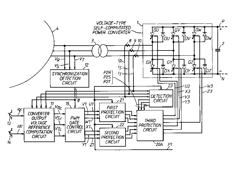
Figure 1 is a circuit diagram illustrating an
embodiment of this invention; only the difference compared
with the conventional example of Figure 4 will be described.
21 is a first protection circuit constituting the first
protection means which turns on the self-turn-off devices,
GU, GV and GW connected to the + (positive) side DC bus line
P of the converter 1 in accordance with the protection
signal P1 from the protective relay element not illustrated,
22 is a second protection circuit constituting the second
protection means which turns off the self-turn-off devices
GX, GY and GZ connected to the - (negative) side DC bus line
N of the converter 1 in accordance with the protection
signal P1 from the protective relay element not illustrated,
and 23 is a detection circuit which detects and generates
detection signal P2R, P2S and P2T when the converter AC
currents have become approximately zero under the condition
that the protection signal P1 from the protection relay
element not illustrated is present. 20A is a third
protection circuit for generating gate signals U3, V3, W3,
X3, Y3 and Z3 to the converter 1.
The construction of the first protection circuit 21,
the second protection circuit 22j the third protection
circuit 20A and the detection circuit 23 will be described
with reference to Figure 2.
-- 10 --
21~5814
In Figure 2, the PWM gate control circuit 15 outputs
the gate signals Ul, Vl, Wl, Xl, Yl and Zl which determine
the conducting periods of the self-turn-off devices GU, GV,
GW, GX, GY and GZ of the converter 1 as in Figure 4.
The first protection circuit 21 is composed of OR
circuits 21U, 21V and 21W. The gate signals Ul, Vl and Wl
from the PWM gate control circuit 15 are applied to first
input terminals of the OR circuits 21U, 21V and 21W,
respectively. The protection signal Pl is applied to second
input terminals of the OR circuits 21U, 21V and 21W. The OR
circuits 21U, 21V and 21W output gate signals U2, V2 and W2,
respectively.
The second protection circuit 22 is composed of AND
circuits 22X, 22Y and 22Z and an inverter circuit 22I. The
gate signals Xl, Yl and Zl from the PWM gate control circuit
15 are applied to first input terminals of the AND circuits
22X, 22Y and 22Z, respectively. The protection signal Pl is
applied to second input terminals of the AND circuits 22X,
22Y and 22Z through the inverter circuit 22I. The AND
circuits 22X, 22Y and 22Z output gate signals X2, Y2 and Z2,
respectively.
The detection circuit 23 is composed of absolute value
detection circuits 231R, 231S and 231T, level detection
circuits 232R, 232S and 232T and AND circuits 233R, 233S and
233T .
The absolute value detection circuits 231R, 231S and
-- 11 --
2115814
231T receive the converter output AC currents iR, iS and iT
detected by the current transformers 8, 9 and 10,
respectively, and detect the absolute values R1, S1 and T1
of the converter output AC currents iR, iS and iT,
respectively. The level detection circuits 232R, 232S and
232T generate detection signals R2, S2 and T2 of the "1"
state when the absolute valves R1, S1 and T1 are below
predetermined values, respectively. The detection signals
R2, S2 and T2 are applied to first input terminals of the
AND circuits 233R, 233S and 233T, respectively. The
protection signal P1 is applied to second input terminals of
the AND circuits 233R, 233S and 233T. Output signals of the
AND circuits 233R, 233S and 233T which are the detection
signals P2R, P2S and P2T are output as the output signals of
the detection circuit, respectively. Namely, the detection
signals P2R, P2S and P2T are generated ~Jhen the converter AC
currents iR, iS and iT have become approximately zero under
the condition that the protection signal P1 is present.
The third protection circuit 20A is composed of AND
circuits 20AU, 20AV and 20AW and inverter circuits 20R, 20S
and 20T. The gate signals U2, V2 and W2 of the first
protection circuit 21 are applied to first input terminals
of the AND circuits 20U, 20V and 20W, respectively.
The detection signals P2R, P2S and P2T of the detection
circuit 23 are applied to second input terminals of the AND
circuits 20U, 20V and 20W through the inverter circuits 20R,
211 ~814
20S and 20T. The AND circuits 20AU, 20AV and 20AW output
gate signals U3, V3 and W3 which are applied to gates of the
self-turn-off devices GU, GV and GW, respectively.
The gate signals X2, Y2 and Z2 of the second protection
circuit 22 are output as the gate signals X3, Y3 and Z3 of
the third protection circuit 20A, which are applied to gates
of the self-turn-off devices GX, GY and GZ, respectively.
In normal state where the protection signal P1 is in
the "0" state, the gate signals U3, V3, W3, X3, Y3 and Z3,
which are equal to the gate signals U1, V1, W1, X1, Y1 and
Z1, are applied to the gates of the self-turn-off devices
GU, GV, GW, GX, GY and GZ to control the conducting periods
thereof, respectively.
In abnormal state where the protection signal P1 is
turned to the "1" state, the gate signals U2, V2 and W2 are
then turned to the "1" state. As the output signals P2R,
P2S and P2T are in the "0" state, the gate signals U3, V3
and W3 are turned to the "1" state, thereby to turn on the
self-turn-off devices GU, GV and GW, respectively. When the
protection signal P1 is turned to the "1" state, the gate
signals X2, Y2 and Z2 are turned to the "0" state. The gate
signals X2, Y2 and Z2 are output as the gate signals X3, Y3
and Z3 thereby to turn off the self-turn-off devices GX, GY
and GZ, respectively.
Then, when the converter AC currents iR, iS and iT have
been approximately zero, the detection circuit 23 generates
~ - 13 -
2ll5814
the detection signals P2R, P2S and P2T of the "1" state. At
this time, the gate signals U3, V3 and W3 become to "O"
state, thereby to turn off the self-turn-off devices GU, GV
and GW, respectively. The gate signals X3, Y3 and Z3
continues to be "O" state, so that the self-turn-off devices
GX, GY and GZ continués to be in the off state.
The operation and effects of this embodimént will now
be explained with reference to Figùre 3. The dashed lines
in Figure 3 show the current-conducting state of the
converter 1 immediately before protection; these are the
same.as the dashed lines in Figure 6, which is for
explaining the operation of the conventional example.
In the situation shown in Figure 3, if the R-phase
current becomes an overcurrent, the self-turn-off devices
GU, GV and GW connected to the + (positive) side DC bus line
P of the converter 1 are first turned on by means of the
first protection circuit 21, and the self-turn-off devices
GX, GY and GZ connected to the - Inegative) side DC bus line
N are turned off by means of the second protection circuit
22, in accordance with the protection signals P1 from the
protective relay not shown in Figure 1.
As a result of this, the R-p~ase current flowing
through the diode DU returns to the AC system 4 through the
turned-on self-turn-off devices GV and GW. Consequently,
the DC capacitor 2 is not charged up and the DC voltage does
not rise. This situation is shown by the solid lines in
- 14 -
21 1581~
Figure 3.
Next, at the moment when the instantaneous value of the
current returning to the AC system 4 has become small, the
detection circuit 23 outputs the detection signals P2R, P2S
and P2T, the self-turn-off devices GU, GV and GW are turned
off by means of the third protectlon circuit 20A, and the
self-turn-off devices GX, GY and GZ continues to be in the
off state, and the protection is completed.
As described above, there is no rise of DC voltage in
the protective shutdown of the voltage-type self-commutated
power converter 1 according to this embodiment.
Up to this point, the explanation has described a 3-
phase voltage-type self-commutated power converter 1, but
this invention can be applied similarly to a single-phase
voltage-type self-commutated power converter. Likewise, a
voltage-type self-commutated conversion system including a
combination of one transformer, one voltage-type self-
commutated power converter and one DC capacitor has been
described in general terms, but the same applies even if it
is a voltage-type self-commutated conversion system with a
number of transformers and voltage-type self-commutated
power converters connected.
According to the voltage-type self-commutated
conversion system of this invention described above, in the
protective shutdown of a voltage-type self-commutated power
converter, the power converter can be shut down safely
- 15 -
-- 2115814
without the DC voltage rising. It can thus be restarted
even if it has been shut down temporarily as a result of,
for example, overcurrent due to AC voltage waveform
distortion. It therefore has the advantages that the
system's essential purpose that is voltage control and
reactive power control of an electrical power system, or
electrical power interchange can be continued and that it
can help to make to the power systems safer.
Obviously, numerous modifications-and variations of the
present invention are possible in light of the above
teachings. It is therefore to be understood that within the
scope of the appended claims, the invention may be practiced
otherwise than as specificàlly described herein.
- 16 -