Note: Descriptions are shown in the official language in which they were submitted.
2~ 1158~
'~_
OVERVOLTAGE PROTECTION CIRCUIT
BACKGROUND OF THE INVENTION
Field of the Invention
This invention relates to an overvoltage
protection circuit, and more particularly to an overvoltage
protection circuit using thyristors with an overvoltage
protection function, an overvoltage protection equipment
constructed with the same and a power converter also
constructed with the same.
SUMMARY OF THE INVENTION
According to one object of this invention there is
provided an overvoltage protection circuit which can finely
adjust the overvoltage protection actuation level, can
prevent the electrical equipment to be protected from
overvoltage from increasing its insulation and the number of
its construction devices and elements and can thereby reduce
the size and production cost of the electrical equipment.
Another object of this invention is to provide an
overvoltage protection equipment which can finely adjust the
overvoltage protection actuation level, can prevent the
electrical equipment to be protected from overvoltage from
increasing its insulation and the number of its construction
-
2 ~ 2
devices and elements and can thereby reduce the size and
production cost of the electrical equipment.
Still another object of this invention is to
provide a power converter wherein its arm has an overvoltage
protection function which can dispense with a separate
overvoltage protection equipment thereof, can finely adjust
the overvoltage protection actuation level, and can thereby
reduce its size and protection cost.
A further object of this invention is to provide a
static var compensator wherein its arm has an overvoltage
protection function which can dispense with a separate
overvoltage protection equipment thereof, can finely adjust
the overvoltage protection actuation level, and can thereby
reduce its size and production cost.
These and other objects of this invention can be
achieved by providing an overvoltage protection circuit
including a plurality of series connected thyristor having
an overvoltage protection function and a plurality of
impedance circuits. Each of the impedance circuits is
connected in parallel with one of the thyristors,
respectively. The impedance circuits include at least a
first impedance circuit having a first impedance value and a
second impedance circuit having a second impedance value
which is different from the first impedance value.
According to one aspect of this invention, there
is provided an overvoltage protection equipment for
protecting an electric equipment from overvoltage. The
overvoltage protection equipment includes three overvoltage
2 ~
protection circuits connected between respective two phases
of the electric equipment. Each of the three overvoltage
protection circuits includes a plurality of series connected
thyristors having an overvoltage protection function and a
plurality of impedance circuits, each of which is connected
in parallel with one of the thyristors, respectively. The
impedance circuits include at least a first impedance
circuit having a first impedance value and a second
impedance circuit having a second impedance value which is
different from the first impedance value.
According to another aspect of this invention,
there is provided an overvoltage protection equipment for
protecting a synchronous motor and a rectifier for supplying
DC power to a field circuit of the synchronous motor from
overvoltage. The overvoltage protection equipment includes
an overvoltage protection circuit connected to the
synchronous motor and the rectifier. The overvoltage
protection circuit includes a plurality of series connected
thyristors having an overvoltage protection function and a
plurality of impedance circuits, each of which is connected
in parallel with one of the thyristors, respectively. The
impedance circuits include at least a first impedance
circuit having a first impedance value and a second
impedance circuit having a second impedance value which is
different from the first impedance value.
According to still another aspect of this
invention, there is provided a power converter including a
plurality of bridge connected arm circults. Each of the arm
2 ~
circuits includes a series circuit of a reactor and an
overvoltage protection circuit. The overvoltage protection
circuit includes a plurality of series connected thyristors
having an overvoltage protection function and a plurality of
impedance circuits, each of which is connected in parallel
with one of the thyristors, respectively. The impedance
circuits include at least a first impedance circuit having a
first impedance value and a second impedance circuit having
a second impedance value which is different from the first
impedance value
According to a further aspect of this invention,
there is provided a tactic var compensator including delta
connected three arm circuits connected between respective
two phases of a power system. Each of the arm circuits
includes a series circuit of a reactor and an overvoltage
protection circuit. The overvoltage protection circuit
includes a plurality of series connected thyristors having
an overvoltage protection function and a plurality of
impedance circuits, each of which is connected in parallel
with one of the thyristors, respectively. The impedance
circuits include at least a first impedance circuit having a
first impedance value and a second impedance circuit having
a second impedance value which is different from the first
impedance value.
For example, we assume that the impedance circuit
respectively connected in parallel with the n thyristors
equipped with overvoltage protection function consist of two
types of impedance circuit of impedance values Zl in one
-- 4 --
8 ~ 2
case and Z2 in the other case (where Zl > Z2). In this way,
by making the impedance values of the impedance circuits
respectively connected in parallel with the n thyristors
equipped with overvoltage protection function different, the
turn-on voltage of the overvoltage protection circuit can be
changed in the range lower than n. WBO.
BRIEF DESCRIPTION OF THE DRAWINGS
A more complete appreciation of the invention and
many of the attendant advantages thereof will be readily
obtained as the same becomes better understood by reference
to the following detailed description when considered in
connection with the accompanying drawings, wherein:
Fig. 1 is a circuit diagram showing an overvoltage
protection circuit according to a first embodiment of this
invention;
Fig. 2 is a circuit diagram showing an overvoltage
protection circuit according to a second embodiment of this
invention;
Fig. 3 is a circuit diagram showing an overvoltage
protection circuit according to a third embodiment of this
invention;
Fig. 4 is a circuit diagram showing an overvoltage
protection circuit according to a fourth embodiment of this
invention;
2 ~
Fig. 5 is a layout diagram showing an overvoltage
protection equipment according to a fifth embodiment of this
invention;
Fig. 6 is a layout diagram showing an overvoltage
protection equipment according to a sixth embodiment of this
invention;
Fig. 7 is a circuit diagram showing a power
converter according to a seventh embodiment of this
invention;
Fig. 8 is a circuit diagram showing a static var
compensator according to an eighth embodiment of this
invention;
Fig. 9 is a layout diagram showing a conventional
overvoltage protection equipment; and
Fig. 10 is a circuit diagram showing a
conventional overvoltage protection circ,uit.
DESCRIPTION OF THE RELATED ART
Fig. 9 is a layout diagram showing an example of a
conventional overvoltage protection equipment using
thyristors equipped with an overvoltage protection function
(hereinbelow called VBO-free thyristors).
In this Figure, 1 is an induction motor, 2 is a
power converter that supplies low frequency AC power to the
secondary circuit of induction motor 1, and 3 is an
overvoltage protection equipment wherein three overvoltage
protection circuits 4 constituted by connecting in series a
. -6
2 ~ 5 ~
plurality of antiparallel connection circuits consisting of
VBO-free thyristors 11 are connected between each phase of
power converter 2. When overvoltage is generated in the
secondary circuit of induction motor 1 by shut-down etc of
the primary side of induction motor 1, the secondary circuit
of induction motor 1 is short-circuited to protect induction
motor 1 from overvoltage.
Fig. 10 is a specific layout diagram of the
conventional overvoltage protection circuit 4 shown in Fig.
9. In this layout, a plurality of antiparallel connection
circuits consisting of VBO-free thyristors 11 connected in
antiparallel are connected in series; snubber circuits
consisting of series circuits of snubber capacitor 12 and
snubber resistor 13 are connected in parallel with the
respective antiparallel connection circuits; and voltage
grading resistors 14 are respectively connected therewith in
parallel.
A VBO-free thyristor 11 is a device which, when a
predetermined prescribed voltage is applied, can perform
turn-on even without a gate signal being applied. Snubber
capacitors 12, snubber resistors 13 and voltage grading
resistors 14 are provided with the purpose of ensuring
uniform voltage sharing between the VBO-free thysistors 11
which are connected in series; their values are the same for
each circuit. If we represent the voltage at which firing
of VBO-free thyristor 11 takes place without application of
a gate signal by W BO, the turn-on voltage in the entire
2 ~ ~85~
series circuit constituted by n VBO-free thyristors 11 is
n. WBO.
In the overvoltage protection equipment 3 shown in
Fig. 9, when the overvoltage protection equipment 3 is
constructed with three overvoltage protection circuits 4
constituted by connecting in series n antiparallel circuits
obtained by antiparallel connection of VBO-free thyristors
11, when the voltage applied to both ends of the overvoltage
protection circuit 4 reaches n.WBO, it is turned ON and
electrical equipment such as inductor motor 1 and power
converter 2 connected to the overvoltage protection
equipment 3 is thereby protected from overvoltage.
However, generally it must be ensured that the
overvoltage protection equipment is not turned ON for the
voltage that is regularly generated by the electrical
equipment, which is connected in parallel with the
overvoltage protection equipment and is to be protected from
overvoltage. Since this regularly ; generated voltage
also includes, for example, surge voltage generated by power
converter shown in Fig. 9, a value higher than the rated
voltage of the electrical equipment that is to be protected
from overvoltage must be selected for the operating voltage
of the overvoltage protection equipment 3. In other words,
a number of VBO-free thyristor 11 antiparallel circuits to
be connected in series must be selected such that the
voltage at which the overvoltage protection equipment 3
turns ON is higher than the regularly generated voltage.
For example, if the regularly generated voltage is more than
n. WBO and less than (n + 0.5).WBO, t~e number of VBO-free
thyristor 11 antiparallel circuits connected in series must
be (n + 1). In this case therefore the overvoltage
protection equipment 3 does not turn ON unless the voltage
applied to the electrical equipment or the voltage generated
in the electrical equipment to be protected from overvoltage
reaches (n + l).WBO. Thus, the electrical equipment that
is to be protected from overvoltage must be capable of
withstanding this (n + l).VVBO voltage. In the case where
the electrical equipment is a power converter, it must have
a higher level of insulation and more number of series-
connected semiconductor devices and other circuit elements
than the level and the number determined by the normal
voltage.
For example, if W BO is 6 kV and the regularly
generated voltage is 13 kV, the number of series-connected
VBO-free thyristor 11 antiparallel circuits to be connected
in series is 3, giving an overvoltage protection equipment
turn-on voltage of 18 kV.
Consequently, although the ideal protection
voltage of the electrical equipment that is to be protected
from overvoltage can be set about 14 kV to 15 kV, the turn-
on voltage of the overvoltage protection equipment is
decided to be 18 kV, so the electrical equipment itself that
is to be protected from overvoltage must be such in terms of
insulation and construction as to be capable of withstanding
18 kV.
2 ~ 5 2
The turn-on voltage of the conventional
overvoltage protection equipment changes in stepwise manner.
If therefore harmonization could not be achieved between the
operating voltage of the overvoltage protection equipment
and the voltage generated by the electrical equipment to be
protected from overvoltage or the voltage applied to the
electrical equipment, size and cost of the electrical
equipment were increased due to the resulting requirement
for further insulation.
The overvoltage protection circuit 4 shown in Fig.
has the function of providing protection for both
polarities of the voltage generated by the electrical
equipment to be protected from overvoltage or voltage
applied to the electrical equipment. However, in cases
where the voltage generated by the electrical equipment to
be protected from overvoltage or voltage applied to the
electrical equipment is a polarity in only one direction,
instead of the VBO-free thyristors 11 needing to be
antiparallel-connected, series connection would surface. In
such cases also, as described above, if harmonization cannot
be obtained between the voltage generated in the electrical
equipment to be protected from overvoltage or voltage
applied to the electrical equipment and the operating
voltage of the overvoltage protection equipment, the
electrical equipment to be protected from overvoltage has to
be unduly large or expensive due to the requirement for
increased insulation.
- 10 -
~ ~ ~ 5 ~ ~ 2 '
DETAILED DESCRIPTION OF THE PREFERRED EMBODIMENTS
Referring now to the drawings, wherein like
reference numerals designate identical or corresponding
parts throughout the several views, the embodiments of this
invention will be described below.
Fig. 1 is a circuit diagram of an overvoltage
protection circuit according to a first embodiment of this
invention that protects from overvoltage of unidirectional
polarity In this Figure, 11-1, 11-2, 11-3 ... ll-n are
VBO-free thyristors, 12-1, 12-2, 12-3 ... 12-n are snubber
capacitors, 13-1, 13-2, 13-3 ... 13-n are snubber resistors
respectively connected in series with each of these snubber
capacitors 12-1, 12-2, 12-3 ... 12-n, and 14-1, 14-2, 14-3
... 14-n are voltage grading resistors respectively
connected in parallel with VBO-free thyristors 11-1, 11-2,
11-3 ... ll-n. Let the combined impedance of snubber
capacitor 12-1, snubber resistor 13-1, and voltage grading
resistor 14-1 be Zl, the combined impedance of snubber
capacitor 12-2, snubber resistor 13-2, and voltage grading
resistor 14-2 be Z2, the combined impedance of snubber
capacitor 12-3, snubber resistor 13-3, and voltage grading
resistor 14-3 be Z3, and the combined impedance of snubber
capacitor 12-n, snubber resistor 13-n and voltage grading
resistor 14-n be Zn. In this invention, different values
are selected for all or some of Zl, Z2, Z3 ... Zn. For
example, if n = 3, Zl : Z2 : Z3 = 1.5 : 1 : 1 or Zl : Z2 :
Z3 = 1.5 : 1.2 : 1 may be selected. To facilitate
- 11 -
~ ~ .~..
~ 2 ~ 8 5 ~
understanding, an overvoltage protection circuit consisting
of three series connections is described below (n = 3). If,
as described above, Zl : Z2 : Z3 = 1.5 : 1 : 1 is selected,
the voltage Vl applied to VBO-free thyristor 11-1 becomes
larger than the voltage V2 applied to VBO-free thyristor 11-
2 and voltage V3 applied to VBO-free thyristor 11-3, and the
21158~2
ratio V1 : V2 : V3 = 1.5 : 1 : 1. If the turn-on voltage of
each of VBO-free thyristors 11-1, 11-2 and 11-3 itself is
VVBO, when VBO-free thyristor 11-1, is ON, the voltage
applied to the series circuits of VBO-free thyristors 11-1,
11-2 and 11-3 is [1 + (1/1.5) + (1/1.5)].VVBO = 2.33 VVBO.
Since this voltage is applied uniformly to VBO-free
thyristors 11-2, 11-3, that is, (2.3/2) W BO = 1.15 WBO is
respectively applied to them, and VBO-free thyristors 11-2
and 11-3 are also successively turned ON. The overvoltage
protection circuit is therefore turned ON at 2.33 WBO.
Also for example if the impedance ratio is selected
such that Z1 : Z2 : Z3 = 1.2 : 1 : 1, the turn-on voltage of
the overvoltage protection circuit can be made [1 + (1/1.2)
+ (1/1.2)]. WBO = 2.66 WBO.- Thus, the voltage at which the
overvoltage protection circuit turns ON can be freely varied
by suitably selecting the impedance ratio, not limited in
S t epwise manner.
According to this embodiment, the electrical equipment
to be protected from overvoltage can be prevented from
increasing its insulation and the number of its construction
devices and elements. Thereby, the electrical equipment can
be reduced in itS size and production cost.
In the first embodiment, snubber capacitors 12-1, 12-2,
12-3, ... 12-n, snubber resistors 13-1, 13-2, 13-3 ... 13-n
and voltage grading resistors 14-1, 14-2, 14-3 ... 14-n were
fixed values, but, as shown in Fig. 2, by making snubber
- 13 -
211S8~2
-
capacitor 15-1, 15-2, 15-3 ... 15-n variable-capacitance
capacitors and by making snubber resistors 16-1, 16-2, 16-3
... 16-n and voltage grading resistors 17-1, 17-2, 17-3 ...
17-n variable resistors, the turn-on voltage of the
overvoltage protection circuit can be even more finely
adjusted.
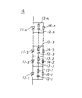
Furthermore, if, in Fig. 1 and Fig. 2, an anti-parallel
connected layout is adopted for VBO-free thyristors 11-1, 11-
2, 11-3 ... 11-n, as shown in Fig. 3 and Fig. 4, an
overvoltage protection circuit that protects from
overvoltage of bidirectional polarity can be produced.
When the voltage that is generated by the electrical
equipment to be protected from overvoltage or the voltage
applied to the electrical equipment is overvoltage of
unidirectional polarity, the overvoltage protection
equipment constructed with the overvoltage protection
circuit of Fig. 1 or Fig. 2 may be connected in parallel
with the electrical equipment that is to be protected from
overvoltage. When the voltage generated by the electrical
equipment that is to be protected from overvoltage or the
voltage applied to the electrical equipment is overvoltage
of bidirectional polarity, an overvoltage protection
equipment constructed with the overvoltage protection
circuit of Fig. 3 or Fig. 4 may be employed.
Such overvoltage protection equipments will be
described with reference to the drawings. Fig. 5 shows an
21158~2
overvoltage protection equipment according to a fifth
embodiment of this invention. In Fig. 5, 18-1 is an
impedance circuit constructed with a series circuit of
snubber capacitor 12-1 and snubber resistor 13-1 and voltage
grading resistor 14-1 connected in parallel with the series
circuit. 18-n is an impedance circuit constructed with a
series circuit of snubber capacitor 12-n and snubber
resistor 13-n and voltage grading resistor 14-n connected in
parallel with the series circuit. In this Figure, the
overvoltage protection equipment 3 is constructed with three
overvoltage protection circuits 4 shown in Fig. 3, which are
connected between each phase of power convertor 2. When
overvoltage is generated in the secondary circuit of
induction motor 1, the secondary circuit is short-circuited
by the overvoltage protection equipment 3 to protect
induction motor 1 from overvoltage.
Fig. 6 shows an overvoltage protection equipment
according to a sixth embodiment of this invention. In Fig.
6, 5 is a synchronous motor and 6 is a rectifier that
supplies DC power to the field winding of synchronous motor
5. In this Figure the overvoltage protection equipment 3 is
constructed with a single overvoltage protection circuit 4
shown in Fig. 3. In this embodiment, when overvoltage is
generated in the field winding of synchronous motor 5, the
field winding is short-circuited by the overvoltage
protection equipment 3 to protect synchronous motor 5 from
2115~52
overvoltage.
In both the embodiments of Figs 5 and 6, a proper
protection voltage can be selected for the turn-on voltage
of the overvoltage protection equipment 3. Accordingly,
prevention of the increase in the insulation of induction
motor 1 and synchronous motor 5 is realized and the number
of series-connected circuit elements in power converter 2
and rectifier 6. Thereby, the size and the production cost
of power converter or rectifier 6 can be reduced.
Fig. 7 shows a power converter according to a seventh
embodiment of this invention. In Fig. 7, 2A is a power
converter constructed with VBO-free thyristors. In this
Figure, power converter 2A is constructed such that each arm
is constructed with a reactor 19 and the overvoltage
protection circuit 4 shown in Fig. 1 or Fig. 2, that is,
each arm itself has an overvoltage protection function.
Fig. 8 shows a static var compensator according to an
eighth embodiment of this invention. In Fig. 8, 7 is a
static var compensator constructed with VBO-free thyristors
11. In this Figure, static var compensator 7 is constructed
such that each arm is constructed with reactor 19 and the
overvoltage protection circuit 4 shown in Fig. 3 or Fig. 4
and has an overvoltage protection function. The static var
compensator 7 is connected to an AC power system to
compensate the reactive power.
In Figs. 7 and 8, an impedance circuit 18 is
- 16 -
2115~52
constructed with a series circuit of snubber capacitor 12
and snubber resistor 13 and voltage grading resistor 14
connected in parallel with the series circuit. Impedance
circuit 18 may be constructed with a series circuit of
variable-capacitance capacitor 15 and variable resistor 16
and variable resistor 17 connected in parallel with the
series clrcuit.
In these embodiments, the overvoltage protection
equipments that were respectively provided in each arm as in
a conventional power converter or a conventional static var
compensator can be dispensed with. The power converter or
the static var compensator according to these embodiments
can finely adjust the overvoltage protection actuation level
as in the overvoltage protection circuit as described above,
and can therely be reduced in its size and production cost.
It should be noted that the arm constituting the power
converter is not restricted to being only an arm in which
VBO-free thyristors 11 are connected in series as shown in
Fig. 7. A power converter could be constructed with an arm
in which there are connected in series a plurality of
circuits consisting of VBO-free thyristors in antiparallel
connection. Furthermore, the power converter is not
restricted to the power converter of Fig. 7. This invention
could also be applied to power converters such as power
converters for cycloconverters, or chopper circuits etc.
In the above-described embodiments, such case has been
- 17 -
21158~2
described that impedance circuit 18 is constructed with a
series circuit of snubber capacitor 12 and snubber resistor
13 and voltage grading resistor 14 connected in parallel
with the series circuit. This invention is not, however,
limited to those embodiments. Any impedance circuit can be
used in this invention, so long as it can change the
respective voltage applied to each of the VBO-free
thyristors 11 connected in series.
As described above, according to this invention even if
an overvoltage protection circuit is constituted by series-
connecting n VBO thyristors whose turn-on voltage is VVBO,
the turn-on voltage of the overvoltage protection circuit
can be made less than n.W BO.
According to this invention, the overvoltage protection
equipment is constructed with the overvoltage protection
circuit as described above. So, the insulation of the
electrical equipment that is to be protected from
overvoltage by the overvoltage protection circuit or
equipment of this invention need not be capable of
withstanding n.W BO, making increased insulation of the
electrical equipment unnecessary. Also, the electrical
equipment need not to increase its construction devices and
elements. Thereby, this invention can reduce the size and
production cost of the electrical equipment to be protected
from overvoltage.
In the power converter or the static var compensator
- 18 -
2115852
according to this invention, the arm itself has an
overvoltage protection function wherein the overvoltage
protection actuation level can be finely adjusted. So, a
power converter or a static var compensator can be provided -
wherein overvoltage protection circuits provided in each arm
can be dispensed with, and can thereby reduce its size and
production cost.
Obviously, numerous modification and variations of the
present invention are possible in light of the above
teachings. It is therefore to be understood that within the
scope of the appended claims, the invention may be practiced
otherwise than as specifically described herein.
-- 19 --