Note: Descriptions are shown in the official language in which they were submitted.
SEI 93-41
TITLE OF THE INVENTION
Schottky Junction Type Field Effec~ Transistor and
Method of Manufacturing the Same
BACKGROUND OF THE INVENTION
Field of the Invention
¦ The present invention relates to a Schottky junc~ion
typ~ field effect transistor (~ESFET) in which a gate
electrode Schot~ky-contacts a semiconductor substrate,
¦ and a method of manufacturing the same.
Related Background Art
As a conventional MESFET of this type, a MESFET
using a GaAs semiconductor material is known. GaAs
MESFETs have been used in a variety of fields such as
high-frequency elements and ultra high-speed ICs. In
applications of GaAs MESFET to these high-frequency ;~
elements and ultra high-speed ICs, GaAs MESFET
characteristics are advantageous in that an output signal
is less distorted in response to an i~put signal.
The voltage vs. current characteristics of a MESFET
generally have so-called square characteristics, and its
drain current Id~ is defined as follows:
~ , , I d8 = K ( Vth -- V~ ) . . . ( 1 ) :
where K is the proportional constant, Vth is the thr~shold
voltage, and V8 is the gate voltage.
Typical square characteristics are shown in a graph
of Fig. 1. The abscissa of this graph represents the gate
'I
;,'~
'7
I SEI 93-41
voltage Vg, and the ordinate represents the drain current
~ Id9 or a transconductance gm. A solid characteristic curve
¦ represents the square characteristics represented by
! equation (1). The ordinate corresponding to this
characteristic curve represents the current Id~ shown on
the left side of Fig. 1. A do~ted characteristic curve
represents a change in transconductance with respect to a
change in voltage of the FET gate voltage having these
I square characteristics. The ordinate corresponding to
this characteristic curve represents the
transconductance g~ shown on the right side of Fig. 1. As
shown in this graph, a change in drain current Id9
exhibits the square characteristics as a function of a
change in gate voltage VB. The drain current Id9 as an
output signal does not change linearly and is distorted
with respect to the gate voltage V~ as an input signal.
This characteristic curve must be linear if the FET
characteristics are less distorted.
To change the square characteristics linearly, i.e.,
to reduce the distortion caused in the output, there is
proposed a structure in which an impurity doping profile
in an active layer must be changed stepwise or gradually
(graded distribution) from a conventional uniform
distribution. An FET having the stepwise impurity
profile of an active layer is disclosed in, for example,
U.S. Patent No. 4,163,984. This prior ar~ describes an
,
'I
0~
SEI 93-41
impurity profile in which an impurity is doped from a
substrate surface to a predetermined depth at a constant
concentration and the impurity concentration increases
stepwise at a pred~termined depth. When an active layer
is formed using this impurity profile, a drain current
linearly changes as a function of a gate voltage.
Therefore~ the output distortion can be reduced.
In the conventional MESFET, however, to change the
impurity profile of the active layer stepwise or in a
¦ 10 graded manner, the following problem is posed.
To realize such a special impurity profile
structure, it is necessary to epitaxially grow an
impurity-doped semiconductor thin film in a predetermined
concentration in accordance with an epitaxial growth
method. Therefore, the impurity concentration for
epitaxially growing a thln film must be precisely
controlled, and an FET having a predetermined impurity
profile must not be easily manufactured.
It is difficult to manufacture FETs having different
threshold voltages Vth on a single wafer because active
layers are formed by the epitaxial growth method, which
greatly limits the design of semiconductor ~ntegrated
circuits. For example, F~Ts constituting an inpu~/ou~put -~
buffer must have the same threshold voltage Vth as that of
FETs constituting a functional section due to thiæ
circuit design limitations.
,.
3 ~
.'.~
..
2 ~
SEI 93-41
j It is possible to recess some gate electrodes to
¦ obtain FETs having a threshold voltage Vth different from
that prior to formation of a recessed structure after
FETs having the same threshold voltage Vth are formed.
However, a method of forming the recess in an active layer
is generally wet etching. This makes it difficult to
uniformly ~orm recesses on a single wafer with good
reproducibility.
In an FET structure having a stepwise or graded
impurity distribution of the active layer, the impurity
concen~ration of the substrate surface is kept low. For
this reason, ohmic contact resistances of source and
drain electrodes formed in contact with this low
concentration layer are set high.
SUMMARY OF THE INVENTION
,_
The present invention has been made to solve the e
~conventional problems described above, and has as its
object to provide a ~ESFET in which linearity of Vg-Id8
characteri~tics can be improved without specifying the
impurity profile o~ an active layer.
In order to achieve the above object of the present
. I , ,
invsntion, there is provided a MESFET arranged such that
an active layer Schottky-contacting a gate electrod~, a
high concentration layer ohmic-contacting a drain
electrode and having a high impurity concentration, and
an intermediate concentration layer formed between the
~' .
- - -
~2 ~ D 8 7
SEI 93-41
, ~.
high concentration layer and the ac~ive layer and having
an impurity concen~ration lower than that of the high
concentration layer are formed in a semiconductor
substrate, wherein the high concentration layer is formed
at a substrate position spaced apart from the gate
electrode by a predetermined distance and has an impurity
concentration and thickness so that a surface depletion
layer generated depending on a surface level on the
drain-side does not almost extend to the drain-side, the
intermediate concentration layer has an impurity
concentration and thickness so that a drain-side end
portion of a channel depletion layer generated upon
. applying a voltage to the gate electrode extends to the
~ drain-side with an increase in this applied voltage, and
..
the high concentration layer, a distance between the high
concentration layer and the gate electrode, and the ~.
l intermediate concentration layer are formed to have a
. relationship in which a ratio of an extension length of a
part of the channel depletion layer from the drain-side
. 20 end portion of the gate electrode to the drain-side end of
the part, to a gate length is 1/5 or more and 1 or lessO
~¦ According to the present invention, there is :
.¦ provided a method of manufacturing the Schottky junction
type field effect ~ransistor, comprising the steps of:
forming an active layer in a surface of a semiconductor
s substrate; forming a dummy gate on the active layer using
; S :,
',
2~1~0~
SEI 93-41
.
a resist; ion-implanting an impurity at a predetermined
f dose and a predetermined acceleration energy using the
dummy gate as a mask, thereby forming a high
con entration layer at least on a drain-side; reducing
outer dimensions of the dummy gate by a predetermined
size; ion-implanting an impurity at a predetermined dose
and a prede~ermined acceleration energy using a reduced
¦ dummy gate as a mask, thereby forming an intermediate
concentration layer having an impurity concentration
lower than that of the high concentration layer on a~
least the drain-side; forming an insulating film on the
dummy gate and then performing a lif~-off process of the
dummy gate to form an inverted pattern at a position where
the dum~y gate was present; and forming a gate electrode
Schottky-contacting the active layer e~posed in ~he
. inverted pattern and a drain electrode ohmic-contacting
the high concentration layer exposed therein.
. According to the present in~ention, there is also
. provided a method of manufacturing the Schottky junction
field e~fect transistor, comprising the steps of: forming
an active layer in a surface of a semiconductor
substrate, forming a gate electrode on the active layer
using a refractory metal, ion-implanting an impu~ity at a
.~ predetermined dose and a predetermined acceleration
energy using the gate electrode as a mask, thereby
iorming an intermediste concentratlon layer on at least a
~60~7
SEI 93-41
drain-side; forming a side wall having a predetermined
¦ thickness on a side surface of the gate electrode on thedrain-side; ion-implanting an impurity at a predetermined
dose and a predetermined acceleration energy using the
gate electrode and the side wall as masks, thereby
forming a high concentration layer having an impurity
concentration higher than that of the intermediate
concentration layer on at least the drain-side; and
forming a drain electrode ohmic-contacting the high
concentration layer.
j The high concentration layer is formed at the
position spaced apart from the gate electrode by a
predetermined distance, and the end portion of the
channel depletion layer extends to the drain-side to some
extent. For these reasons, a rate of increase in drain
current with an increase in gate voltage can be lowered.
That is, a long gate effect tends to occur. On the other
hand, the intermediate concentration la~er having the
predetermined impurity concentration and thickness is
formed between the high concentration layer and the
active layer Schottky-contacting the gate electrode to
suppress extension of the end portion of the channel
depletion layer toward the drain-side. A change in drain
current tends to occur with a change in gate voltage in
accordance with the square characteristics. Therefore,
the long gate effect and the effect for changing the drain ~.
.:~
2 ~ 7
i
SEI 93-41
i current in accordance with the square characteristics
cancel each other. For this reason, tAe drain current
linearly changes with a change in gate voltage, an FET
output changes linearly in response to an input, and
output distortion can be eliminated.
The high and intermediate concentration layers ~an
be formed by the ion-implantation method, and an
epitaxial growth method using precise impurity control
need not be used. For this reason, an FET free from
outpu~ distortion can be easily manufactured. Use of tha
ion-implantation method facilitates selective formation
of the high and intermediate concentration layers on the
substrate. Accordingly, FETs having different threshold
voltage~ can be formed on a single substrate. In
addition, the impurity concentration on the substrate
i surface has a value enough to achieve a'sufficiently low
ohmic-contact resistance. Therefore, ~he contact
resistance of the ohmic electrode can be sufficiently
reduced.
According to the present invention, as described
~i above, linearity of the drain current as a function of
`I gate voltage can be improved even in a MESFET ha~ing an
ion-implanted impurity profile. Therefore, the present
invention can be effectively used for a basic element for
a circuit such as a high-power signal amplifier which
requires a small output signal distortion in response to
,~
~6~7
,.
SEI 93-41
an input signal.
The present invention will become more fully
understood from the detailed description given
hereinbelow and the accompanying drawings which are given
by way of illustration only, and thus are not to be
considered as limiting the present invention.
Further scope of applicability of the present
invention will become apparent from the detailed
description given hereinafter. However, it should be
understood that the detailed description and specific
examples, while indicating preferred embodiments of the
invention, are given ~y way of illustration only, since
various changes and modifications within the spirit and
scope of the invention will become apparent to those
skilled in the art form this detailed description.
BRIEF DESCRIPTION OF THE DRAWINGS
.. . .
Fig. 1 is a graph showing typical square
characteristics of a MESFFT;
Figs. 2 to 4 are sectional views showing the steps in
the manufacture of the MESFET according to the first
embodiment of the present in~n~ion;
Figs. 5 to 7 are sectional views for explaining
operations of the first embodiment according to the
present invention;
::
Figs. 8 and 9 are graphs showing ~3-Id8 and Vg8-gm
characteristics obtained in correspondence with an FET
I
~ .
] ~ `~
0 ~ 7
:~
SEI 93-41
shown in Figs. 5 to 7;
Fig. 10 is a graph for explaining the concept of
linearity of the FET according to the present invention;
Fig. 11 is a graph showing Vg-g~ characteristics
i~ using a side-etch amount as a parameter in the MESFET
having a structure of the first embodiment;
Fig. 12 is a graph showing V~-gm chara~teristics
using a gate length as a parameter in the MESFET having
3l the structure of the first embodiment;
Fig. 13 is a graph showing the relationship ~etween
a gate length Lg and a side-etch amount Lgn+ to obtain a
highly linear FET when nt- and n'-type layers are formed
under specific conditions;
I Fig. 14 is a graph showing the relationship between
an Si dose and side-etch amount L8_n+ to obtain a highly
.,l linear FET when an n+-type layer is formed under specific
I conditions;
,~ . Fig. 15 is a graph showing the relation~hip between
.¦ a peak carrier concentration and a side-etch amount L8_n+
to obtain a highly linear FET when an n~-type layer is
.l formed under specific conditions;
'I
Fig. 16 is a graph showing the relationship between -~
, an Si dose and side-etch amount L~n+ to obtain a highly
. linear FET when an n'-type layer is formed under specific
conditions;
.¦ Fig. 17 is a graph showing the relationship between
~` 10
.~
: ~'
., .,
1 2 1 1 6 ~) ~3 7
SEI 93-41
a peak carrier concentration and a side-etch amount Lg_n+
to obtain a highly linear FET when an n'-type layer is
formed under specific conditions;
Figs. 18 to 20 are sectional views showing the steps
in the manufacture of ~he MESFET according to the second
embodiment of the present invention;
Figs. 21 to 25 are sectional views showing the steps
in the manufacture of the MESFET according to the third
embodiment of the present invention; and
Fig. 26 is a sectional view showing an FET structure
having another formation position of an n'-type layer.
DBTAILED DESCRIPTION OF THE PREFERRED EMBODIMENTS
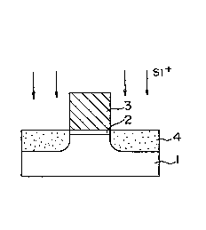
Figs. 2 to 4 are sectional vi~ws showing the method -
of manufacturing a GaAs MESFET according to the first
embodiment of the present invention.
Si ions are implanted to an FET formation region on a
semi-insulating GaAs semiconductor substrate 1. By this
ion implantation, an active layer 2 containing an n-type
impurity in a predetermined concentration is formed to
have a predetermined thic~ness on the substrate surface.
A resist is spin-coated on the active layer 2 and a gate
pattern is transferred to the resist to form a dummy gate
3. Then, Si ions are implanted using the patterned dummy
gate 3 as a mask to form an n+-type layer (high
concentration layer) 4 (Fig. 2). This ion implantation
, for forminy the n+-type layer 4 is performed at an
' 11
~'
~''~ '
.
, .
.
2 ~ 7
SEI 93-41
acceleration energy of 90 keV and a does of 2 x 10l3
[ l/cm2] .
The outer dimensions of the dummy gate 3 are
isotropically reduced by reactive ion etching (RIE) using
an 02 plasma. ~s a result, the active layer 2 covered with
~ the dummy gate 3 is partially exposed. Si ions are
;1 implanted again using a reduced dummy gate 3a as a mask.
This ion implantation is performed at an acceleration
energy of 30 keV and a dose of 3 x 10¹² [l/cm2]. An n'-type
layex 5 is formed in the e~posed portion of the active
layer 2 by this ion implantation (Fig. 3). The width of
this n'-type layer 5 is determined by the degree of
reduction of the dummy gate 3, i.e., a side-etch amount
Lg_n+~ This side-etch amount Lgn+ determines a distance
between the n+-type layer 4 and a gate elec~rode (to be
described later).
After an SiO2 film is deposited on the entire surface
of the qubstrate 1 using sputtering, the reduced dummy
gate 3a is lifted off. By this lift-off process, an
inverted pattern i5 formed on an SiO2 film 6 at a trace of
the dummy gate 3a. Thereafter, annealing for activating
the implanted Si ions is performed. Then, a gate
electrode 7 to Schottky-contact the e~posed active layer
2 is formed on the inverted pattern using Ti/Pt/Au
metals. After the SiO2 film 6 on the n+-type layer 4 is
selectively removed, a source electrode 8 and a drain
.,~
g o ~ ~
~:~
SEI 93-41
electrode 9, which respectively ohmic-contact the n~-type
layer 4,i~re formed using Au/Ge/Ni metals (Fig. 4). As a
result, a MESFET is completed.
In the ME5FET according to this embodiment, the
n~-type layer 4 is formed at a substrate position apart
from the gate electrode 7 by the d stance of the side-etch
amount L8n+. In addition, the n+-type layer 4 has an
impurity concentration and thickness such that a surface
depletion layer generated depending on a surface level on
the drain-side does not almost extend to the drain-side.
, .
Accordingly, the influence of the surface depletion layer
on a channel depletion layer can be reduced, and movement
of electrons flowing in a current channel is controlled
by the channel depletion layer without being influenced
by the surface depletion layer.
The n'-type layer 5 as an intermediate concentration
layer having a lower impurity concentration than that of
the n+ layer 4 has an impurity concentration and thickness
such that a drain-side end portion of a channel depletion
,!,~ 20 layer generated upon applying a voltage to the gate
~ electrode 7 extends to the drain-side with an increase in
,.j ~ ~ , ,
this applied voltage. Moreover, the n~-type layer 4, a
distance L~_n+ between the n+-type layer 4 and the gate
electrode 7, and the n'-type layer 5 are formed to have a
,j relationship in which a ration of an extension length L of
i!' a part of the channel depletion layer from the drain-side
i`
~ 13
.
.: .~. ,~.......... . . .
8 7
SEI 93-41
end portion A of the gate electrode 7 to the drain-side
end of the part, to a gate length L~ is to fall within a
predetermined range.
In a MESFET having a ga~e length of 1 ~m or less, a
considerably strong electric field is generated in the
drain-side of the depletion layer. If a MESFET is formed
using a material (e.g., GaAs) having a lot of surface
levels, a source resistance increases on the source side,
and the channel depletion layer extends outward on the
drain-side, as compared with the actual gate. A "long
yate effect" which effectively increases a gate length is
caused. For this reason, in a conventional structure, an
n~-type region self-aligned with a gate electrode is
formed in a source/drain region, thereby eliminating the
influences of the surface level.
In a MESFET having a side-etch amount L8_n.t = shown
in Fig. 5, an n~-type layer 11 is self-aligned with a gate
electrode 12, and ~he gate electrode 12 is adjacent to the
n+-type layer 11 on the drain-side. For this reason,
although the influence of the surface level can be
eliminated, a channel depletion layer 13 does not extend
toward the drain-side. The voltage vs. current
characteristics of this MESFET exhibit square
characteristicq represented by a solid curve 21a in the
~ graph of Fig. 8, thereby causing output distortion. In
i this case, the abscissa represents the gate voltage V~
SEI 93-41
[V], and the ordinate represents the drain current Id8
[A]. The transfer function characteristics of the MESFET
are represented by a solid curve 21b in the graph of
Fig. 9, and the g~ value cannot be kept constant upon a
ch~nge in gate voltage. In this graph, the abscissa
represents the gate voltage V~9 ~V] ~ and the ordinate
represents the transconductance g~.
To solve this problem, a distance of a side etch
amount LB_n+ ~ 0 is set between the gate electrode 14 and
the n+-type layer 5, as shown in Fig. 6. If an MESFET
having no n'-type layer is arranged, a channel depletion
layer 16 extends considerably on the drain~side. In
contrast, the long gate effect is caused. That is~ +he
voltage vs. current characteristics of the MESF~T are
represented by a chain double-dashed-line curve 22a in
the graph of Fig. 8. A rate of increase in drain current
with an increase in gate voltage is reduced, and
linearity is low. In addition, the transfer function
characteristics of the ~ESFET are represented by a chain
double-dashed~line curve 22b in the graph of Fig. 9, and
the gm value cannot be kept constant upon a change in gate
voltage.
To the contrary, in a MESF~T having an n'-type layer
¦ by assuring a predetermined distance in the side etch
. amount L~_n+~ i.e., in a MESFET schematically shown in
Fig. 7, the above inconvenience does not occur. The
lS
., .
2 ~ 7
SEI 93-41
structure of the drain-side impurity region in the MESFET
according to this embodiment employs an LDD (Lightly
Doped Drain) structure. In addition, in this LDD
structure, the n+-type layer 4 is formed appropriately
away from the gate electrode 7, tha impurity
concentration of the n'-type layer 5 is lower than that of
the n~-type layer 4 by a predetermined amount. The
thickness of the n'-type layer 5 is smaller than that of
the n+-type layer 4 by a predstermined amount. That is,
the distance between the gate elec~rode 7 and the n+-type ~-
layer 4 and the impurity concentrations and thicknesses
of the n+- and n'-type layers 4 and 5 are optimized
relative to each other. For this reason, a channel
., .
depletion layer 10 extends appropriately on the drain-
side, and the voltage vs. current characteristics of the
MESFET are xepresented by a chain-line curve 23a in the
graph of Fig. 8.. The drain current changes linearly with
a change in gate voltage, and output distortion can be
; eliminated. The transfer function characteristics of the
i~ 20 MESFET are represented by a chain-line curve 23b in the
graph of Fig. 9, and the g~ ~alue i5 kept constant upon a
change in gate voltage.
: In this embodiment, the n+-type layer 4 is formed
~ : .
apart from the gate electrode 7 by the distance Lg_n+~ and
the n'-type layer 5 has the predetermined impurity
concentration and thickness. For these reasons, the end
s 16
i~ :
,: ~
SEI 93-41
portion of the channel depletion layer tends to e~tend
~;~ toward the drain side to some extent. As a result, a rate
of increase in drain current with an increase in gate
3 voltage is reduced. That is, the long gate effect tendsto occur. On the other hand, the impurity concentration
and thickness of the n'-type layer 5 formed between the
active layer 2 and the n+-type layer 4 are set to suppress
extension of the end portion of the channel depletion
.
j layer on the drain-side, and the drain current tends to~l lO change with a change in gate voltage in accordance withthe square characteristics. Therefore the long gate
effect and the effect for changing the drain current in
accordance with the s~uare characteristics cancel each
other. A~ a result, the change in drain current with a
chanye in gate voltage becomes linear, and an output
signal from the F~T linearly corresponds to an input
signal. Unlike the conventional case, the output
distortion can be eliminated.
In this embodiment, the linearity of the MESFET is
considered as follow~. A graph in Fig. lO represents a
change in transconductance g~ with a change in gate
voltage ~. The abscissa in this graph represents the
gate voltage V~ ~V], and the ordinate represents a ratio
g~/g ~ of the transconductance g~ to a maximum
transconductance g~. A charac~eristic curve in Fig. lO
represents a change in conductance ratio g~/g~ with a
.~ .
17
,
, 1
~i
0 ~3 7
.~,
SEI 93-41
change in gate voltage Vg when a drain-source voltage Vd8
is kept constant, e.g., 3.0 V. The maximum
transconductance g~ represents a maximum value of the
transconductance g~ of ~he characteristic curve. A range
of transconductances gr~having values as 90% or more of
the maximum transconductance ~r~ iS defined as VliD~ar as
shown in Fig. 10. I?n the compound semiconductor FET such
as a GaAs MESFET, the gate voltage V8 will not be set at
0.6 V or more (V3 > 0.6 V), and an in~erval between the
threshold voltage Vth of the FET and the voltage of 6 V is
defined as Vp as shown in Fig. 10. The threshold voltage
Vth is a gate voltage in which a current channel formed in
the active layer 2 pinches off. For example, if the
threshold voltage Vth of the FET is -2.0 V, Vp is given as
2.6 V.
According to thi3 embodiment, when the ratio of the
J~ linear voltage range Vlln~r ~o the application voltage
range Vp of an FET is 50~ or more (Vll"ear/VP ~ 0-5) within
~ the applied drain voltage (an applied voltage between a
X 20 source electrode and a drain electrode) of 0.5 V to 10 V,
','! this FET is regarded as a highly linear element. In a
highly linear MESFET having the ratio Vllna~r/Vp of 50~ or
more, the gain of a former-stage amplifier using
~` small-signal amplification can be s~abilized. When the
h, ratio Vllna~r/Vp is set to 70~ or more, the distortion of a
~ pcwer amplifier which amplifies a large signal can be
?,
.` 18
,'',~'1 ' ' "
.,,,1
21161)87
SEI 93-41
reduced.
In general, a MESFET having the following impurity
profile has a ratio VIlDear/Vp of 50% or more and serves as a
highly linear element. That is, when a high
concentration layer corresponding to the n~-type layer 4
and the intermediate concentration layer corresponding to
the n~-type layer 5 are formed by ion implantation for a
MESFET having a gate length Lg from 0.1 um to 2.0 ~u, the
peak concentration of the high concentration layer having
the maximum impurity concentration is 1 ~ 10l8 [lJcm3] or
more and a substrate depth a~ which an impurity
concentration is 1 x 10l7 [1/cm3~ is 0.1 ~m or more and
0.25 ~m or less . At the same time, the peak
concentration of the intermediate concentration layer is
1 ~ 10l7 [1/cm3~ or more and a substrate depth at which a
:
concentration is 1 x 10l~ [lJcm3] is set to 0.20 ~m or
less. In addition, the side-etch amount Lgn~ is set to
; fall within the range of 0.1 ~m to 2.0 ~m. An FET having
this impurity profile is highly linear to obtain the same
effect as in the above embodiment. In this case, when the
depth from the substrate surface is plotted along the
. , ~ ~
abscissa and the carrier concentration is plotted along
the ordinate in such a manner that the substrate depth
increases away ~rom the origin along the abscissa and the ; -
concentration increases away from the origin along the
ordinate, the impurity profiles of the high and
19
~ SEI 93-41
:i
intermediate concentration layers are almost inverted
parabolic profiles. More specifically, the peak of the
impurity concentration is located at a depth slightly
lower from the substrate surface. When the substrate
depth further increases, the impurity concentration
parabolically decreases. The substrate position having
the impurity concen~ration of 1 ~ 10l7 [1/cm3] or 1 x 10l8
[l/cm3] is deeper than that of the peak impurity
concentration.
A graph in Fig. ll shows a change in ~`
transconductance wi~h respect to a change in a gate
voltage using a side-etch amount Lg-n~ as a parameter in
the MESFET structure having a gate length L~ of 0.5 ~m and
a gate width Wg of 20 ~m according to this embodiment. The
abscissa in this graph represents a gate-source voltage
(gate voltage) V~a tV], and an interval between scale
marks is 0.250/div. The ordinate of the graph in Fig. 11 -~
represents a transconductance gm, and an interval between
the scale marks is 1.0/div.
The side-etch amount L8n+ as a parameter changes
every 0.07S ~m in an order of 0.15 ~m, 0.225 ~m, 0.30
~m,.... Characteristic curves 31, 32, and 33 correspond
to side--etch amounts Le_~+ of 0.15 ~m, 0.225 ~m, and 0.30
~m, respectively. ~s is apparent from this graph, in an
FET having a gate length of 0.5 ~m~ the transconductance
gm hecomes kept constant even with a change in gate
. ;~:
. ~ .
SEI 93-41
voltage when the side-etch amount Lg_n+ becomes about 0.30
~m. It is thus understood that linearity of the drain
current change characteristics with a change in gate
voltage can be improved.
A graph in Fig. 12 shows a change in
transcondu tance as a function of the gate voltage using
a gate length L8 as a parameter in the MESFET structure
having a gate width Wg of 20 ~m and a side-etch amount Lg_n+
of 0.30 ~m according to this embodiment. The abscissa in
d lo ~his graph represents a gate voltage Vg9 [V], and aninterval between scale marks is 0.2500/div. The ordinate
of the graph in Fig. 12 represents a transconductance gm,
and an interval between the scale marks is 1.000/div.
The gate length L8 as a parameter changes in an order
of 0.5 ~m, 1.0 ~m, 1.5 ~m, 2.0 ~m,.... Characteristic
curves 41, 42, 43, and 44 correspond to the gate lengths
of 0.5 ~m, 1.0 ~m, 1.5 ~m, and 2.0 ~m, respectively. As
is apparent ~rom this graph, even when the side-etch
amount L8_n~ becomes about 0.30 ~m, if the gate length
becomes longer, the transconductance g~ cannot be kept
constant. It is thus understood that linearity of the
drain current change characteristics with a change in
gate voltage is degraded~
To eliminate an output distortion, it is underætood
from these drawings that the side-etch amount Lgn~ i.e.,
~I the extension length L of the part of the channel
.
; O ~ ~
SEI 93-41
depletion layer 10, which extends *rom the drain-side end
portion A of the gate electrode 7 to the drain-side, and
the gate length L8 must be set to have a predetermined
ratio. In addition, it is considered from these drawings
that a ratio L/L~ of an extension L of the channel
depletion layer 10 to the drain-side to the gate length LB
may be se~ 1/S or more and 1 or less.
When the side-etch amount LR_n~ is larger than the
side-etch amount Lgn~ - 0.30 ~m at which the g~ value is
kept in constant, constancy of the g~, i.e., linearity of
the voltage vs. current charac~eristics i5 degraded. In
this case, if the n'-type layer 5 is not formed between
the active layer 2 and the n+-type layer 4, the channel
depletion layer 10 may extend to the drain-side to an
extent almast equal or more to the side-etch amount. At
this time, a ratio L/Lt of an extension L to the drain-
side to the gate length L8 i~ 0.6 (= 0.3j0.5) or more. The
upper limit of the ratio L/~8 can be 1 with a certain
maryin because the channel depletion layer 10 slightly
extends into the n~-type layer 4. On the other hand, the
lower limit of the ratio L/L8 may be empirically ;~
determined to be 1/5 on the basi~ of the graphs described
.
above.
If the relationship between the gate length Le and
the side-etch amount LBn~ is defined in a graph of Fig. 13
under specific manufacturing conditions, it is
.
22
'
.,.
,
ly~
SEI 93-41
empirically known that an FET having good linearity can
be obtained. The specific manufacturing conditions are
conditions in which an n-~ype impurity is ion-implanted
at an acceleration energy of 90 to 120 keV and a dose of
4.0 ~ 10l3 [1/cm2] through an 800+50A thick SiN film to
form the n+-type layer 4, and an n-type impurity is
ion-implanted at an acceleration energy of 50 keV and a
dose of 6.0 x 1ol2 [1/cm2] through an 800~50A thick SiN
film to form the n'~type layer 5. To further improve the
linearity of the FET, the FET threshold voltage Vth is set
lower than -1.5 v to widen the linear voltage range Vllnear.
For thi~ purpose, 2asi~ is ion-implanted direct to the
substrate at an acceleration ener~y of 30 keV or more to
form the active layer 2. In addition, 9Be~ is also
. ion-implanted direct to the ~ubstrate at an acceleration
energy of 70 keV or more to obtain a steep carrier profile
. at the substrate interface between the active layer 2 and
the ~ubstrate 1~ When these manufacturing conditions are
applied to the FET manufacturing process of the above
. ZO embodiment, the SiN films through which ions are
implanted are ~ormed after the active layer 2 and the
.
dummy gate 3 are formed. Ion-implanting operations are
performed after such SiN films are formed, thereby
satisfying the speci~ic manufacturing conditions.
The abscissa in this graph represents the gate
length L8 [~m], and the ordinate represents the side-etch
'
23
;~
SEI 93-41
amount Lt3n+ [~m]. In a first curve 71 shown in ~his graph,
the side-etch amount Lent+ gradually increases in the range :
of 0 to about 0.8 ~m with an incrtase of 0 to about 1.5t~m
in the gate length Lg. In a second curve 72, the side-etch
t~mount Lt~n+ gradually increases in the range of 0 to about
1.5 ~m with an increase of 0 to about 1.5 ~m in the ga~e
length L~. According to the experiences of the applicant,
if the relationship between the gate length Lg and the
side-etcht~mount Lg~,t~ is defined in a hatched area in this
graph in which the first curve 71 is the lower limit and
: the second curve 72 is the upper limit, it is empirically
known that an FET having good lintParity can be obtained.
t~hat is, if the relationship between the gate length Lg
, and the side-etch amount Lg_nt is set in a hatched area in
;~ this graph, and ~he specific manufacturing conditions are
applie~ to the above et~bodiment to manufacture the
~ESFET, a highly linear FET is obtained, thereby ,~
obtaining the same efftect as.in the abovetembodiment.
~.,
Assume that the gate length L,3 is 0.8t~m and that ion
implantation for the n~-type layer 4 is performed at an
acceleration energy of 90 to 120 keV and a dose of 4.0 x
1013 cm~2 through an 800+50A thick SiN film. In addition ,,
the n'-type layer S is formed under the conditions ,~,'
represented in a graph of Fig. 14, it is empirically known .
s that a highly linear element can be obtained. Ion
~. implantation is also performed through an 800~t~toA thick
:
,
! 2~L
.,,., ' "'
,
'`'I ~:
~i
,..,i
:,~
SEI 93-41
SiN film to form ~his n'-type layer 5. The abscissa in
the graph of Fig. 14 represents a dose ~cm~2] of Si~ ions,
and the ordinate represents a side-etch amount L8_n+ [~m].
Characteristic curves 81 and 82 in this graph
re~pectively represent relationships between the Si doses
of 50 and ~0 keV and the side-etch amount Le_n~. The
characteri~tic curves 81 and 82 represent that the
side-etch amounts L~_n+ gradually increase within the range
of about 0 to about 1.2 ~m with an increase in dose of 10l2
to 10l3 cm~2, using the acceleration energy as a parameter.
When ion implantation for the n'-type layer 5 is
performed under the condition that the relationships
between the Si doses, the acceleration energies, and the
side-etch amounts are conditions represented by the
characteristic curves 81 and 82 to manufacture the FET of
the above embodiment, a highly linear FET, i.e., an FET
~` satisfying condition V~ r/Vp > 0.7 is obtained, thereby
, obtaining the same effect as in the above embodiment.
When the n~-type layer 4 is formed under the specific
conditions described above, and the n'-type layer 5 is
formed in accordance with the relationship shown in
Fig. 14, the relationship between the peak carrier
concentration and the side etch amount Lg_~ of the n'-type
layer 5 i9 shown in Fig. 15. The abscissa of this graph
represents the peak carrier concentration ~l/cm3] of the
n'-type layer 5, and the ordinate represents the
,`, I
,~
o ~ ~
SEI 93-41
side-etch amount IJ8-Q+ [~m] thereof. First and second
curves 91 and 92 represent the relationships between the
peak carrier corlcentrations and ~he side-etch amounts Lg_
when the depth of the n'-type layer S having a carrier
concentration of 1 x 10¹³ tl/cm3~ from the substrate
surface is used as a parameter. More specifically, the
first curve 91 represents the relationship between the
peak carrier concentration and the side-etch amount L8n+
using as a parameter a substrate depth of 0.13 ~m at which
the carrier concentration of the n'-type layer 5 is 1 x
0l8 [1/cm3]. The æide-etch amount Lg_n+ gradually
increase~ within the range of 0 to about 1.0 ~m with an
increase in peak carr.ier concentration in the range of 1 x
1017 ~1/cm3] to 1 x lOla [l/cm3]. The second curve 92
represents the relationship between the peak carrier
concentration and the side-etch amount L8n+ using as a
t parameter a ~ubstrate depth of 0~20 ~m at which the
carrier concentration of the n' type layer 5 is 1 x 10l-3
~l/cm3] . The side~etch amount L~ n+ gradually increases
within the range of about 0.2 to about 1.5 ~m with an
increase in peak carrier concentration in the range of 1 x
1O17 [1/cm3] to 8 X 1O17 [1/Cm3].
The first and second curves 91 and 92 represent that
the substra~e depth at which the carrier concentra~ion is
~lJcm3~ corresponding to a specific peak carrier
concentration = x (1ol7 to 1018 [1/cm3] ) and a specific
26
'~;
'
4 ,~
? ~ 16087
;
SEI 93--41
æide-etch amoun~ LB_n+ = y (0 to 1.5) fall within the range
of 0.13 to 0.20 ~m. That is, when the n+-type layer 4 is
formed under the specific conditions described above and
the n'-type layer S is formed in accordance with the
relationship shown in Fig. 14, the relationship between
the peak carrier concentration, the substrate depth at
which to ~he carrier concentration is 1 x 101~ [1/cm3] ~ and
I the side-etch amount Lg_n+ falls within a hatched area
between the first and second curves 91 and 92 shown in
Fig. 15. TherefOre, an FET having V~in~Ar/Vp > 0-7 can be
obtained.
Assume that the gate length L8 is 0.8 ~m and tha~ ion
implantation for the n'-type layer 5 is performed at an
acceleration enersy of 50 keV and a dose of 6.0 x 10l2 cm~g
through an 800+50A thick SiN film. In addition the
n+-type layer 4 is ~ormed under the conditions represented
in a graph of Fig. 16, it is empirically known that a
highly linear element can be obtained. Ion implantation
i~ also performed through an 800+50A thick SiN film to
~orm this n+-type layer 4. The abscissa in the graph of
Fig. 16 represents a dose rcm~2] of Si+ ions, and the
ordinate represents a side-etch amount La_n+ [~m].
Characteristic curves 101 and 102 in this graph
~; respectively represent relationships between the Si doses
of 70 and 90 keV and the side-etch amount Lg_n+~
Characteristic curve 103 represent relationship between
Z7
.1
a s 7
;~
SEI 93-41
the Si dose of 120 keV and the side-etch amount Lg_n+~ The
characteristic curves 101, 102, and 103 represent that
the side-etch amounts L~n~ gradually increase within the
range of about 0 to about 0.8 ~m with an increase in dose
of 10l3 to 10~4 cm~2, using the acceleration energy as a
parameter. When ion implantation for the n+-type layer 4
is performed under the condition that the relationships
between the Si doses, the acceleration ~nergies, and the
side-etch amount L8n+ are conditions represented by the
characteristic curves 101, 102, and 103 to manufacture
the FET of the above embodiment, a highly linear FET is
obtained, thereby obtaining the same effect as in the
above embodiment.
When the n'-type layer 5 is formed under the
specific conditions described above, and the n+-type
layer 4 i~ ~ormed in accordance with the relationship
shown in Fig. 16, the relationship between the peak
carriar concentration and the side-etch amount Lg_n+ of the
n~-type layer 4 is shown in Fig. 17. The abscissa of this
graph represents the peak carrier concentration [1/cm3]
of the n+-type layer 4, and the ordinate represents the
side-etch amount Lg_n+ ~m] thereof. First and second
cllrves 111 and 112 represent the relationships between
; the peak carrier concen~rations and the side--etch amounts
L~_n+ when the depth of the n~-type layer 4 having a carrier
concentration of 1 x 1ol7 [1/cm3] from the substrate
`j 28
J
~ .
$ ~
SEI 93-41
surface is used as a parameter. More specifically, the
first curve 111 r~presents the relationship between the
peak carrier concentration and the side~etch amount LKnt
using as a parameter a substrate depth of 0.15 ~m at which
the carrier concentration of the n+-type layer 4 is 1
7 [1/cm3]. The side-etch amount Lg_n+ gradually
increases within the range of about 0.05 to about 0.35 ~m
with an increase in peak carrier concentration in the
range of 1 x lOla ~l/cm3] to 1 x 1ol9 [1/cm3]. The second
curve 112 represents the relationship between the peak
carrier concentration and the side-etch amount LRn+ using
as a parameter a substrate depth of 0.25 ~m at which the
carrier concentration of the n+-type layer 4 is 1 x 10l7
~l/cm3]. The side-etch amount L~_n+ gradually increases
within the range o~ about 0.~5 to about 0.65 ~m with an
increase in peak carrier concentration in the range of 1 x
10l8 ~1/cm3~ to 1 x 10la [1/cm3].
The first and second curves 111 and 112 represent
that the sùbstrate depth at which the carrier
` 20 concentration is 1 x 10l7 [l/cm3] corresponding to a
specific peak carrier concentration = x (1018 to 10l3
, ~ ! [l/cm3]) and a specific side~etch amount Lg_n~ = y (0.05 to
0.65) fall within the range of 0.15 to 0.25 ~m. That is,
when the n'-type layer S is formed under the specific
conditions described above and the n+-type layer 4 is
formed in accordance with the relationship shown in
29
,~1
.1 ` ' .
.;!
' 7
,.
SEI 93-41
Fig. 16, the relationship between the peak carrier
concentration, the substrate depth corresponding to the
carrier concentration of 1 x 10l7 tl/cm3~, and the
side-etch amount L~n+ falls within a hatched area between
the first and second curves 111 and 112 shown in Fig. 17.
Therefore, an FET having Vline~r/Vp > 0.7 can be obtained.
The MESFETs described with reference to Figs. 13 to
'~ 17 are FETs having the following impurity profile in
accordance with the manufacturing conditions described
above. That is, when ion implantation is performed at a
dose of 4.0 x 10l3 [1/cm~i] through an 800+50A thick SiN
film to form the n+-type layer 4, the peak carrier
concentration of the n+-type layer 4 is 1 x lola [1/cm3~ or
more and 1 x 10la [1/cm33 or less. When ion implantation
. i9 performed at an acceleration energy of 90 to 120 keVthrough an 800~50A thick SiN film to form the n+-typ~
layer 4, the depth having the carrier concentration of 1 x
1017 ~1/cm3] from the substrate surface is 0.15 ~m or more
and 0.30 ~m or less. ~hen ion implantation is performed
at a do~e of 6.0 x 10l3 ~1/cm2] through an 800+50A thick
SiN film to form the n'-type layer 5, the peak carrier
concentration o~ the n'-type layer 5 is 1 x 10l7 [1/cm3] or
, more and 1 x 10l3 ~1/cm3] or less. When ion implantation
is performed at an acceleration energy of 50 keV through
an 800~50A thick SiN film to form the n'-type 5, the depth
having the carrier concentration of 1 X lol6 [1/cm33 from ~r
i;
O g 7
I
SEI 93-41
the substrate surface is 0.15 ~m or less.
In the MESFET according to the above embodiment, the
n~-type and n'-type layers 4 and 5 are formed by the ion
implantation~ For this reason, the epitaxial growth
method using precise impurity control need not be used.
Therefore, according to the method of manufacturing an
FET in this embodiment, an FET ~r~e from output
distortion can be easily manufactured. Use of the
ion-implantation method facilitates selective formation
of the n~-type and n'-type layers 4 and 5 on the
substrate. That is, a resist can be used as a mask to an
FET group of one region on a wafer, and a predetermined
impurity profile can be formed by ion implantation to an
FET group of another region. Therefore, FETs having
various types of threshold voltages Veh can be formed on a
3ingle wafer, thereby solving the conventional
limitations upon ~esign of semiconductor integrated
, circuitq. That is, FETR having characteristics necessary
for respective portions of the integrated circuits are
easily formed. Since an active layer need not be recessed
¦ by etching to obtain different threshold values, ~ETs
.I with good reproducibility and uniformity can be obtained.
i Since the source and drain electrodes 8 and 9 are formed
'i , , .
to contact the n+-type layer 4 having a sufficiently high
impurity concentration, ohmic contact resistances can be
sufficiently reduced. Therefore, unl1ke in a
31
.~
2 ~ 8 7
¦ SEI 93-41
conventional FET having an impurity profile formed in a
I stepwise or graded manner, the problem that the impurity
concentration of the substrate surface is lowered and
that the ohmic con~act resistances can not be
~ufficiently reduced does not occur.
The second embodiment of the present invention will
be described below. Figs. 18 to 20 are sectional views
showing the method of manufacturing a MESFET according to
the second embodiment of the present invention.
Si ions are implanted to an FET formation region on a
semi-insulating GaAs semiconductor substrate 51. By this
ion implantation, an active layer 52 containing an n-type
impurity in a predetermined concentration is formed to
have a predetermined thickness on the substrate surface. -
Then, a refractory metal, e.g., a WSi~, is deposited on
the active layer 52. A gate pattern is formed on this
refractory metal using the normal photoresist technique.
The refractory metal is etched by RIE using the gate
pattern to form a gate electrode 53. Si ions are
implanted under given conditions using this gate
electrode 53 as a mask to form an n'-type layer 54 as an
intermediate concentration layer (see Fig. 18).
An SiOa film is deposited on the entire surface of
the substrate using the atmospheric pressure CVD method.
The deposited SiO2 film is selectively removed by RIE to
form a side wall 55 on the side surface of the gate
. .
32
.
2~0~7
SEI 93-41
electrode 53. Si ions are implanted in ~ high
concentration using the gate electrode 53 and the side
wall 55 as masks to form an n+-type layer 56 (Fig. 19). A
distance L~-D+ between the gate electrode 53 and the
n+-type layer 56 is adjusted to a desired distance by
setting the thickness of the side wall 55.
l, After the side wall 55 is selectively removed, an
`i ohmic-electrode pattern is formed on the substrate
surface using the normal photolithography. A source
electrode 57 and a drain electrode 58, which respectively
¦ ohmic-contact the n+-type layer 56, are formed using this
pattern (Fig. 20). As a result, a MESFET is completed.
¦ In the MESFET according to this embodiment, the
n+-type layer 56 is formed at a substrate position apart
l ~rom the gate electrode 53 by the distance Lg_n~
¦ corresponding to the thickne3s of the side wall 55. In
addition, the n+~type layer 56 has a predetermined
impurity concentration and thickness so that a surface
depletion layer generated depending on a surface level on
the drain-side does not almost extend to the drain-side.
Accordingly, the influence of the surface depletion layer
on a channel depletion layer can be reduced, and movement
of electrons flowing in a current channel is controlled
..
by the channel depletion layer without being influenced
by the surface depletion layer.
The n'-type layer 54 as an intermediate
33
~ . .
~:
.' ~ ,r~
`:~
3 SEI 93-41
concentration layer having a lower impurity concentration
~3 than that of the n~ layer 56 has an impurity concentration
and thickness such that a drain-side end portion of the
channel depletion layex generated upon applying a voltage
to the gate Plectrode 53 extends ~o the drain-side with an
increase in this applied voltage. Moreover, the n+-type
layer 56, the distance L8_n+ between ~he n+-type layer 56
and the gate electrode 53, and the n'-type layer 54 are `~
for~ed to have a relationship in which a ratio of an
e~tension length of the drain-side end portion of the :
channel depletion layer from the drain-side end portion
of the gate electrode 53 to the drain-si~e, to a gate
length L~ is 1/5 or more and 1 or less.
In the MESFET according to the second embodiment,
the drain current Id8 linearly changes with a change in ~:
gate voltage V~, and output distortion can be eliminated ;-~
as in the fîrst embodiment. In this embodiment, an FET is
formed ~y the ion implanta~ion, and the epi~axial growth
method need not be used unlike in a conventional FET,
.~ 20 thereby easily manufacturing an FET. FETs having
different threshold voltages can be formed on a single
l~ wafer, and ohmic contac~ resistances can be sufficiently
`¦ reduced, thereby obtaining the same effect as in the
;l ,
first embodiment.
~.1 In the description of each of the above embodiments,
.~
3 the n'-type and n+-type layers respectively on the source
34
",I
,~
~3 :
21160~7
SEI 93-41
and drain-sides are formed symmetrically. However, the
structure on the drain-side is the characteristic feature
of the present invention. Therefore, the structure on
the source side is not limited to the structure of each of
the above embodiment.
Ne~t, the third embodiment according to the present
invention will be egplained hereinbelow. MESFET
according to the third embodiment has a structure in
which an ion implantation in a source side and an ion
implantation in a drain side are non-symm~trical to each
ot~er with respect to a gate electrode. Figs 21-25 are
sectional view showing the method of manufacturing the
GaAs MESFET according to the third embodiment of the
present invention.
An ion-implantation to an FET formation region on a
semi-insulating GaAs semiconductor substrate 131 i5
per~ormed. In the ion-implantation, Sl+ions are
implant4d direct to the substrate at an acceleration
energy of 50 KeV and a dose of 5 x 101~ [l/cm2]. By this
ion implantation, an active layer 132 containing an n-
type impurity in a predetermined concentration is formed
to have a predetermined thickness on the substrate
surface (see Fig. 21). Besides, Be+ ions may be implanted
to form a buried p-type layer at this time.
Next, a SiN layer 133 having thickness of 800~50A is
formed on the substrate surface. Thereafter, a resist is
.:
.
~1
--`~
6 ~ ~ 7
SEI 93-41
spin-coated on this SiN layer 133 and a n~region
formation pattern is transferred on the resist 134. A . -:
length of the resist 134 is set to be 1.8 ~m as shown in
the Drawing. Then An ion implantation is performed using
this resist 134 as a mask and a source region 135 and a
drain region 136 which are n+layers (high concentration
layers) are formed (see Fig. 22). The ion implantation
for formation of this n+layer is performed at
acceleration energy of 120 Kev and a dose of 4 x 10¹³
[1/cm2] through the SiN layer 133.
Next the resist 134 on the substrate surface is
removed and a new resist is coated on the SiN layer 133.
The coated resist i~ patterned with a predeteirmined shape
and a dummy gate 137 i5 formed at a position shifted near
a source side. The length of the dummy gate 137
corresponds to that of a gate electrode (gate length)
referred below and is set to be 0.8 ~m.'By the position
of the dummy gate 137, a distance L8n+between the gate
electrode referred below and a gate side end portion of
the drain region 13~ is set to be 0.85~m. Next Sition is
implanted using the dummy gate 137 as a mask so that n'
.,1 . I
`.j layers 138 and 139 which are intermediate concentration
layers, are formed (~ee Fig. 23). An ion implantation for
~ formation of the n' layers 138 and 139 is performed at an
i I . acceleration energy of 50 KeV ~nd a dose of 6 x 10
L1/cm2J through the SiN layer 133.
36
::1
7 --.
8 7
.,
`!
:! SEI 93-41
Next a SiO2 layer 138 having a thickness of 300 A is
l deposited on the substrate surface by a sputtering and
I thereafter, ~he dummy gate 137 is lifted off. By the
¦ lift-off process, an inver~ed pattern is formed on the
j SiO2 layer 138 at a trace of the dummy gate 137 (s0e Fig.
~ 24). Thereafter, annealing process having the annealing
¦ temperature of 870 C and the annealing time of 5 seconds
is performed for activating the implanted ion. Then a
gate electrode 140 to Schottky-contact the expo~ed active
layer 132 is formed on the inverted pattern using --
Ti/Pt/Au metals. After the SiO2 layer 138 on the source
region 135 and the drain region 136 is selectively
removed, a source electrode 141 and a drain electrode
142, which respectively ohmic-contact the source region
135 and the drain region 136, are formed using Au/Ge/Ni
metals (see Fig. 254). As a result, MESFET in which n'
.
layers are formed non symmetrically is completed.
In the MESFET of this embodiment, a gate length
thereof i~ set to be 0.8 ~m, the length o the n' layer
138 positioned near the source region 135 is set to be
0.15 ~m and the length of the n' layer 139 positioned near
the drain~region 136 is set to be 0.85 ~m. That is, the
distance between the gate electrode 140 and a gate side
edge of the source region 135 is short and the source
region 135 is formed near the gate electrode 140.
Accordingly in M~SFET of the third embodiment, the high
37
.
,
Q ~ 7
., .
SEI 93-41
linearity of the FET output with respect to an input
thereto can be realized by employment of the above
structure of the n' layer 139 positioned near the drain
region 136 and the drain region 136. Accordingly in the
third embodiment, the advantageous effect obtained in the
first and second embodiments can be obtained and further
the source resistance can be e~tremely reduced by the
above struc~ure of the n' layer 138 near the source
~ region 135 and the source region 135 and as the result,
";
high speed operation and high range output can be
, realized also.
In the description of each of the above embodiments,
GaAs is used as a substrate material. However, the
present invention is not limited to this. For example, an
InP material, an InGaAs material, or the like may be used
to ~orm the FET. The same ef~ect as in each of the above
embodiments can be obtained. Also, in the description of
each of the above embodiments, Si is used as an n-type
impurity. However, Se, S, or the like may be used as an
~ 20 n-type impurity. The same effect as in each of the above
ii embodiments can be obtained using these materials.
In the descrip~ion of the structure according to
each of the above embodiments, as shown in a schematic
,
view of Fig. 7, the gate electrode 7 is adjacent to the
n'-type layer 5 on the drain-side. However, the gate
- electrode 7 is not necessarily adjacent to the n'-type
.:
38
.,
, !
$
SEI 93-41
layer 5. Since the linearity of the MESFET is determined
by the extension of the depletion layer on the drain-
side, the n'-type layer 5 is formed at a substrate -
position slightly spaced apart from the gate electrode 7
by a distance a, as shown in Fig. 26. Notie that the same
reference numerals in Fig. 26 denote the same parts as in
Fig. 7, and a description will be omsittedO In such a
s~ructure, the same effect as in each of the above
embodiments can be ob~ained.
10From the invention thus described, it will be ;~
obvious that the invention may be varied in many ways.
Such variations are not to be regarded as a departure from
the spirit and scope of the invention, and all such
modifications as would be obvious to one skilled in the
art are intended to be included within the scope of the
following claims.
,
.
~: '
:, '
, . ' ' '~
: .. '
. .'
.
.. ,