Note: Descriptions are shown in the official language in which they were submitted.
WO94/01930 PCT/US93/0562~
~1 i6582
RF AMPL~ER BIAS CONTROL METHOD AND APPARATUS
Field of -he Invention
The present invention relates generally to RF
amplifiers and more particularly to RF power
amplifiers.
Background of the Invention
RF power amplifiers are used in a wide variety
of co~lln-cations and other electronic
applications. These amplifiers are made up of one
or more cascaded amplifier stages, each of which
increases the level of the signal applied to the
input of that stage by an amount known as the stage
gain. Ideally, the input to output transfer of
each stage is linear; a perfect replica of the
input signal increased in amplitude appears at the
amplifier output. In reality, however, all power
amplifiers have a degree of non-linearity in their
transfer characteristic. This non-linearity
adversely effects various amplifier operating
characteristics such as gain performance,
intermodulation performance and efficiency.
Non-linear amplifier transfer characteristics
gives rise to a phenomenon, hereinafter referred to
as gain expansion. Gain eXpAnsion is caused by the
change in the amplifier's base-emitter voltage due
to rectification of input signal power in the base-
emitter junction. In effect, the input signal
power to an RF amplifier changes the amplifier's
quiescent operating point. As a result, an RF
~ ~ 165 8 2
- 2
amplifier's gain will increase as a function of the input signal power, thereby
giving rise to the gain expansion phenomenon. Gain expansion is typically an
undesirable characteristic exhibited by RF power amplifiers. This is especially
true when the amplifier must operate across a wide dynamic range of input
signals, like the multi-tone linear power amplifiers disclosed in C~n~ n Patent
Application Serial No. 2,109,506, filed January 27, 1993, entitled HIGH
DYNAMIC RANGE MODULATION INDEPENDENT FEED FORWARD
AMPLIFIER NETWORK and assigned to the assigned to the assignee of the
present application. In such multi-tone applications, constant amplifier gain
over a wide dynamic range of input signals is required.
This same non-linearity causes distortion of the amplifier's output signal
so that it is no longer a perfect replica of the input signal. This distortion
produces spurious signal components known as intermodulation products.
Intermodulation products are typically undesirable because they cause
interference, cross talk, and other deleterious effects on the performance of a
system employing the amplifier. Of note, the quantity of intermodulation
products generated by the amplifier is directly proportional to the magnitude ofthe signal applied to the amplifier's input.
Yet another RF power amplifier operating characteristic hampered by
non-linear transfers is the amplifier's efficiency. By definition, an amplifier's
efficiency is determined by POUT/PIN The more efficient an amplifier is, the less
input power required to achieve a desirable output level. Since gain expansion
tends to distort the amplifier's output power level, it has the undesirable effect
of decreasing an amplifier's efficiency at low output powers.
Accordingly, the prior art reflects various methods and devices designed
to improve one or more of the amplifier's operating characteristics, typically at
the expense of others. As will be appreciated, optimi7.ing for any one parameteradversely effects the others, since they are all closely interrelated. Thus, while
biasing the amplifier's quiescent operating point low tends to improve the
amplifier's efficiency, intermodulation performance and saturation point, it
nonetheless compromises the maximum gain available and the amplifier's gain
~L ~
2 1 1 6 5 8 2
- 3 -
flatness (constant gain over wide dynamic range). Conversely, while biasing
the amplifier's quiescent operating point higher tends to improve the maximum
gain available and the amplifier's gain flatness, it nonetheless compromises theamplifier's efficiency, intermodulation performance and saturation point.
It would be extremely advantageous therefore to provide a compensation
circuit capable of equ~ ing an RF power amplifier's operating characteristics
over a wide dynamic range of inputs, while avoiding the shortcomings of the
prior art.
Summary of the Invention
In accordance with the present invention, there is provided a bias control
circuit for use with an RF amplifier having a plurality of operating performancecharacteristics responsive to a quiescent operating point established by the RF
amplifier bias current. The circuit comprises means, coupled to an RF
amplifier, for detecting a DC current drawn by the RF amplifier; and means,
coupled to the detecting means, and the RF amplifier, for adjusting the RF
amplifier bias current as a function of the detected DC current, to control the
RF amplifier's quiescent operating point and thereby optimize the RF
amplifier's operation for selected operating performance characteristics.
Brief Der~ ,lion of the Drawings
FIG. 1 shows a first embodiment of an RF amplifier bias control circuit
in accordance with the present invention;
FIG. 2 shows a second embodiment of an RF amplifier bias control
circuit in accordance with the present invention;
FIG. 3 shows yet a third embodiment of an RF amplifier bias control
circuit in accordance with the present invention;
FIG. 4 depicts the transfer function of the bias control circuits in
accordance with FIGS. 1, 2 and 3; and
FIG. 5 depicts an exemplary sign~lling environment anticipated by the
amplifier networks of FIGS 1-3.
Detailed Description of the Preferred Embodiment
Referring to FIG. 1, there is shown in block diagram form, an RF
~;.7~,,
2~ ~ô5~2
- 4 -
amplifier network 100 according to the present invention. An exemplary
sign~lling environment for this network is depicted in FIG. 5.
W094/01930 PCT/US93/0562
As shown in FIG. 5, network 100 signalling
anticipates both narrow bandwidth modulated input
signals 510 and wide bandwidth modulated input
signals 520, such as, for example, a Frequency
Division Multiple Access (FDMA) format and/or a
Code Division Multiple Access (CDMA) format. In
addition to comprising multiple modulation formats,
the proposed signalling environment of the RF
amplifier network 100 is further characterized by
input signals which exhibit a wide dynamic range of
input power levels.
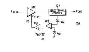
Referring back to FIG. 1, the RF amplifier
network 100 includes an RF amplifier 102,
directional coupler 104, DC amplifier 106, DC
inverting amplifier 108 and diode detector 112.
During operation, the RF input signal PIN is
amplified by the RF amplifier 102 in order to
provide an amplified output signal POUT. A portion
of the amplified output signal is routed to the DC
amplifier 106 via directional coupler 104 and diode
detector 112 which converts the RF output power
level POUT to a DC voltage. The DC amplifier 106
compares the converted DC signal to a reference
Vref and amplifies the difference. This amplified
difference signal is then routed to DC inverting
amplifier 108 which is configured so as to provide
a decreasing bias voltage Vbias to the RF amplifier
102 as the amplifier output power level POUT
increases, thereby adjusting the amplifier bias
current as a function of the output power level, in
order to control the amplifier's quiescent
operating point. The Zenor diode VREF acts as a
reference for this inversion. As will be
appreciated, VREF may be tailored so as to adjust
the slope of the dynamic bias transfer curve
WO94/01930 ~ 582 - 6 - rCT/US93/0562
injected into the RF amplifier 102 along path 110,
as shown in FIG. 4.
Referring to FIG. 2, there is shown in block
diagram form, a second embodiment of an RF
amplifier network 200 according to the present
invention. The RF amplifier network 200 includes
an RF amplifier 202, resistor R1, DC amplifier 206,
Zenor diode VREF, and DC inverting amplifier 208.
During operation, the output power POUT of the RF
amplifier 202 is detected as a function of the
collector current, I Collector, injected into the
RF amplifier 202 along path 20~. As will be
appreciated, the collector current is directly
proportional to the output power of an RF amplifier
202. In this effort, the resistor R1, in circuit
with supply voltage Vcc is employed as an I
Collector current sensor.
In accordance with the preferred embodiment,
R1 is a very low impedance resistor, typically .05-
1 ohm in value. This impedance tends to produce avoltage drop across R1, that while detectable, is
small enough to avoid degradation of the overall
amplifier performance. In accordance, the voltage
drop is amplified by the DC operational amplifier
206 and routed to DC inverting amplifier 208.
Inverting amplifier 208 is so configured in
order to provide a decreasing bias voltage Vbias to
the RF amplifier 202 as the output power POUT
increases, thereby adjusting the amplifier bias
current as a function of the output power level, in
order to control the amplifier's quiescent
operating point. The Zenor diode VREF acts as a
reference for this inversion. As will be
appreciated, VREF may be tailored so as to adjust
WO94/01930 ~ 2 PCT/US93/0562
the slope of the dynamic bias transfer curve
injected into the RF amplifier 202 along path 210.
Referring to FIG. 3, there is shown yet
another embodiment of an RF amplifier network 300
according to the present invention. The RF
amplifier network 300 operates substantially in
accordance with the description provided with FIG.
1, except that the RF amplifier bias current is
adjusted as a function of the RF input signal power
level, P~N, as opposed to the RF output signal power
level, POUT. A directional coupler 312 routes the
RF input signal PIN to the bias control circuit
306-310 which operates to provide a decreasing bias
voltage, Vbias, to the RF amplifier 302 as the
amplifier input power level PIN increases, thereby
adjusting the amplifier bias current as a function
of the input power level, in order to control the
amplifier's quiescent operating point.
It will be appreciated by those skilled in the
art that FIG. 4 depicts the transfer function of
the bias control circuits of FIGS. 1, 2 and 3.
In summary, the overall effect of the various
bias control circuits described herein are to
increase the bias voltage to an RF amplifier during
low output power levels, while decreasing the bias
voltage of the RF amplifier during high output
power levels in order to overcome the phenomenon of
gain expansion and to optimize the amplifier's
operation for selected operating performance
characteristics like intermodulation performance
and efficiency.
What is claimed is: