Note: Descriptions are shown in the official language in which they were submitted.
CA 02116766 1998-03-18
SOLDER BUMP FABRICATION METHOD AND SOLDER BUMPS FORMED
THEREBY
Field of the Invention
This invention relates to microelectronic device
manufacturing methods and more particularly to methods of
forming electrical and mechanical connections for a
microelectronic substrate, and the connections so formed.
Background of the Invention
High performance microelectronic devices often use
solder balls or solder bumps for electrical
interconnection to other microelectronic devices. For
example, a very large scale integration (VLSI) chip may
be electrically connected to a circuit board or other
next level packaging substrate using solder balls or
solder bumps. This connection technology is also
referred to as "Controlled Collapse Chip Connection - C4"
or "flip-chip" technology, and will be referred to herein
as "solder bumps".
In the original solder bump technology developed by
IBM, the solder bumps are formed by evaporation through
openings in a shadow mask which is clamped to an
integrated circuit wafer. Solder bump technology based
on an electroplating process has also been actively
pursued, as, for example, described in Edward K. Yung &
Iwona Turlik, "Electroplated sQlder Joints for Flip-Chip
Applications," IEEE Trans. Comp. Hybrids & Man. Tech.,
Vol. 14, No. 3, September 1991. Electroplated solder
bumps are typically used in integrated circuit chips
requiring a large number of connections. In the
electroplating process, an "under-bump metallurgy" (UBM)
is deposited on a microelectronic substrate having
contact pads thereon,
'
,.
CA 02116766 1998-03-18
__
usually by evaporation or sputtering. A continuous
under-bump metallurgy film is typically provided on the
pads and on the substrate between the pads, in order to
allow current flow during solder plating.
Alternatively, a plating base composed of a material
that is not wettable by solder (e.g., chromium) may be
deposited across the contact pads and the substrate
between contact pads, with individual pads of under-
bump metallurgy deposited on top of the chromium film
over the contact pads.
In order to define the sites for solder bump
formation over the contact pads, the sites of the
solder bumps are photolithographically patterned, by
depositing a thick layer of photoresist on the under-
bump metallurgy and patterning the photoresist to
expose the under-bump metallurgy over the contact pads.
Solder pads are then formed on the exposed areas of the
under-bump metallurgy, over the contact pads, by
pattern electroplating. The plated solder accumulates
in the cavities of the photoresist, over the contact
pads. Then, the under-bump metallurgy between the
plated solder pads is etched, using the solder as an
etch mask, to break the electrical connection between
the solder bumps. The photolithographic patterning and
under-bump metallurgy etching steps define the geometry
of the under-bump metallurgy at the base of the solder
bump, between the solder bump and the contact pad.
Solder bump fabrication methods are described in U.S.
Patents 4,950,623 to Dishon, assigned to the assignee
of the present invention; 4,940,181 to Juskey, Jr. et
al.; and 4,763,829 to Sherry.
Unfortunately, in fabricating solder bumps
using the process described above, it is difficult to
preserve the base of the solder bump, at the contact
~,
CA 02116766 1998-03-18
'_~
2a
pad. Preservation of the base is important because the
base of the solder bump is designed to seal the contact
pad. The process described above often reduces the
base, which exposes the underlying contact pad and
leads to mechanical and/or electrical failure.
The base may be reduced due to at least two
steps in the above described process. First, there is
often an inherent distortion of the patterned thick
~ gn~en~ wic~ res_ec~
CA 02116766 1998-03-18
to the contact pads lying thereunder. Typically, a dry
-thick film photoresist (such as du Pont RISTON~
photoresist) or multiple coatings of liquid photoresist
is used, in order to accumulate sufficient volume of
- 5 plated solder. Thicknesses on the order of tens of
microns (for example 50 microns) are used. The thic~
film photoresist must be accurately patterned over the
contact pads, without misalignment or distortion.
Unfortunately, for dry film photoresist,
distortion of the shape of bump sites may result from
the relatively poor adhesion of the photoresist to the
smooth under-bump metallurgy. Light scattering through
the thick film photoresist and cover layer, and the
imprecise nature of the thick film photoresist
development process, also contribute to distortion of
the photoresist mask pattern over the contact pads.
For multiple-layer liquid photoresist, factors such as
hardening of photoresist due to long periods of baking,
and edge bead build-up, may cause distortion in the
photoresist mask pattern over the contact pads.
Accordingly, the resultant solder bump often does not
cover the entire contact pad.
The second major factor which may reduce the
solder bump base is undercutting during chemical
etching of the under-bump metallurgy. In particular,
as described above, the under-bump metallurgy is
typically etched, between the solder bumps, in order to
break the electrical connections therebetween. In
order to insure that all of the unwanted under-bump
metallurgy is removed, overetching typically needs to
be practiced, because etching frequently does not
proceed uniformly across the substrate surface.
However, this overetching typically undercuts the
under-bump metallurgy between~the solder bump and the
contact pad, which reduces the solder bump base.
Electrical and mechanical reliability of the solder
bump connection is thereby degraded.
,. ...
CA 02116766 1998-03-18
.._ j
Summary of the Invention
It is therefore an object of the present invention
to provide an improved method of forming solder bumps for
microelectronic device connections, and improved solder
bumps formed thereby.
In accordance with an aspect of the present
invention there is provided a method of forming solder
bumps on a plurality of contact pads on a substrate,
comprising the steps of :
forming an under-bump metallurgy on the contact pads
and on the substrate between the contact pads; then
forming thick film solder retaining walls on the
substrate between the contact pads, the solder retaining
walls exposing the under-bump metallurgy over the contact
pads; then ~ .
forming solder pads over the contact pads, on the
under-bump metallurgy which is exposed by the solder
retaining walls, then
reflowing the solder pads to form solder bumps
having an intermetallic layer of the under-bump
metallurgy and the solder adja~ent the contact pads; and
then
etching the under-bump metallurgy between the
contact pads; the improvement characterized by:
adding the step of forming thin film solder dams on
the under-bump metallurgy between the contact pads prior
to the step of forming solder retaining walls, the solder
dams exposing the under-bump metallurgy over the contact
pads and the retaining walls being formed on the solder
dams; and
replacing the etching step with the step of etching
the solder dams and the under-bump metallurgy between the
contact pads, with at least one etchant which etches the
intermetallic layer more slowly than said solder dams and
the under-bump metallurgy, to the solder bumps adjacent
the contact pads.
CA 02116766 1998-03-18
4a
.._
According to another aspect of the present invention a
method for forming solder bumps on a plurality of contact pads
on a substrate, which comprises the steps of:
forming an under-bump metallurgy on the contact pads and
S on the substrate between the contact pads; then
forming solder on the under-bump metallurgy over the
contact pads, with the under-bump metallurgy between the
contact pads being free of solder; then
converting at least part of the under-bump metallurgy
over the contact pads into an intermetallic layer of the
under-bump metallurgy and the solder, by reflowing the solder;
and then
removing the under-bump metallurgy between the contact
pads while preserving the intermetallic layer over the contact
pads, to thereby reduce undercutt$ng of the reflowed solder.
These and other objects are provided,
according to the present invention by reflowing or
melting the solder pads prior to etching the under-bump'
metallurgy between the solder pads. An intermetallic
layer of the under-bump metallurgy and the solder is
thus formed between the solder bump and the contact
pad, at the base of the solder bump, prior to etching
the under-bump metallurgy. Accordingly, at least part
of the under-bump metallurgy layer between the solder
bump and contact pad is converted to an intermetallic
of the solder and the under-bump metallurgy, prior to
etching the under-bump metallurgy. Preferably, when
the under-bump metallurgy includes a top layer of
copper, and lead-tin solder is used, substantially all
of the top copper layer is converted to an
intermetallic of copper and tin.
The intermetallic layer is resistant to
etchants which are used to etch the under-bump
metallurgy. The under-bump metallurgy may therefore be
removed between the contact pads, while preserving the
intermetallic layer at the base of the solder bump.
Accordingly, minimal undercutting of the solder bumps
is produced so that the base size is preserved and the
CA 02116766 1998-03-18
_
--5--
contact pads are not exposed. Electrical and
mechanical reliability of the solder bump connection is
thereby enhanced.
The invention also reduces misalignment
between the solder pads and its underlying contact
pads, and tolerates distortion in patterning the solder
accumulation layer. In particular, a continuous under-
bump metallurgy is formed on the contact pads and on
the microelectronic substrate between the contact pads.
Solder dams are then formed on the under-bump
metallurgy between the contact pads such that the
solder dams expose the under-bump metallurgy over the
contact pads. The exposed uncer-bump metallurgy over
the contact pads define the location of the solder bump
base. During reflow, the solder will retract or spread
to these areas.
The solder dams, also referred to as solder
stops, are preferably formed ~rom a thin film layer (on
the order of 1 micron or less)~ such as a thin film of
chromium (on the order of 1500A thick), which adheres
well to the under-bump metallurgy. The solder dams are
precisely aligned to the underlying contact pads using
known integrated circuit photolithography. The solder
dams are preferably patterned~using a lift-off
technique, although other photolithographic techniques
may be used to pattern the solder dams.
Solder retaining walls are then formed on the
solder dams. These walls, which may be formed of thick
film (on the order of 50 microns) photoresist, need
only accumulate solder volume. They need not be used
for alignment purposes, becau$e the solder dams provide
precise alignment. Accordingly, misalignment and
distortion of the thick film solder retaining walls
will not reduce the base of the solder bump over the
CA 02116766 1998-03-18
contact pads. Solder pads ar.e then electroplated onto
the substrate over the contact pads, on the areas of
Che unoer bu~p me-al_ul~y~ which _
/
/
i' A
CA 02116766 1998-03-18
",,,_ .
exposed by the solder dams an~ solder retaining walls.
The solder retaining walls may then be removed.
Then, prior to removing the under-bump
metallurgy between the contac~ pads, the solder is
reflowed (melted) to form a solder bump having an
intermetallic layer of the solder and the under-bump
metallurgy at the base of the solder bump adjacent the
contact pad. For example, when the topmost component
of the under-bump metallurgy is copper and conventional
lead/tin solder is used, a copper/tin intermetallic is
typically formed. During reflow, the solder dams
prevent lateral spread and bridging of the solder, and
control the size of the bump base.
The solder dams and under-bump metallurgy are
then etched to isolate the solder bumps, using at least
one etchant which etches the intermetallic layer more
slowly than the solder bumps and under-bump metallurgy.
Since the intermetallic has been formed at the base of
the solder bumps, the bumps are relatively unaffected
by the etchant. In particular, a mixture of ammonium
hydroxide with trace amounts of hydrogen peroxide may
be used to etch copper, and a hydrochloric acid based
etchant may be used to etch chromium. Neither of these
etchants is effective against the copper/tin
intermetallic.
The base of the solder bumps formed according
to the present invention is not reduced by under-bump
metallurgy etching or solder pad
misalignment/distortion. By preserving the base
geometry, mechanical and electrical reliability is
enhanced.
Moreover, it has been found that there is a
lateral reaction between the solder pad and the under-
bump metallurgy during the reflow step of the present
~ ,, . ~,
CA 02116766 1998-03-18
~ ,_
6a
invention. Accordingly, the-intermetallic layer formed
CA 02116766 1998-03-18
--7--
to form a lip around the base of the solder bump. This
lip provides extra protection for the edge of the
solder bump and the edge of the contact pad underneath
the solder bump. Accordingly, the invention produces a
new profile of solder bump, which improves mechanical
and electrical reliability.
Brief Des~ lio" of the Drawings
Figures 1-5 illustrate cross-sectional views
of a microelectronic substrate during fabrication of
solder bumps thereon according to the present
invention.
Figure 6 is a scanning electron microscope
photograph of a solder bump formed according to the
present invention.
Detailed Des~ lio,~ of a r, ef~"ed Gnl.o~li"~ent
The present invention now will be described
more fully hereinafter with reference to the
accompanying drawings, in which a preferred embodiment
of the invention is shown. This invention may,
however, be embodied in many different forms and should
not be construed as limited to the embodiment set forth
herein; rather, this embodiment is provided so that
this disclosure will be thorough and complete, and will
fully convey the scope of the invention to those
skilled in the art. Like numbers refer to like
elements throughout.
Referring now to Figure 1, there is
illustrated a microelectronic substrate 10 having a
plurality of contact pads 12 thereon. It will be
understood by those having skill in the art that
microelectronic substrate 10 may be an integrated
circuit chip, a circuit board or microelectronic
packaging substrate, or any other substrate which
requires electrical and mechanical connection. Contact
pads 12 are formed on substrate 10 using well known
techniques which need not be described herein. The
contact pads are typically aluminum for integrated
2'' ~
CA 02116766 1998-03-18
--8--
circuit chips, although other metals and metal
composites may also be used for integrated circuit
chips and other substrates.
As also shown in Figure 1, a passivating
dielectric 14 is formed on the substrate 10 and
patterned to expose the contact pads 12, using
conventional plasma or reactive ion etching or other
well known patterning techniques. A continuous under-
bump metallurgy 16 is then formed on the substrate over
the contact pads 12 and between the contact pads 12.
As is well known to those having skill in the art, the
under-bump metallurgy 16 typically contains a (bottom)
chromium layer (about loooA thick) adjacent
substrate 10 and pads 12, which functions as an
adhesion layer and diffusion barrier for the under-bump
metallurgy. A top copper layer (about 1 micron thick)
is typically provided to act as a solderable metal, and
a phased chromium/copper layer (about loooA thick) is
formed between the chromium and copper layers. The
under-bump metallurgy may be formed by conventional
thin film deposition techniques such as evaporation or
sputtering, and need not be described further herein.
Referring now to Figure 2, a solder dam or
solder stop layer 18 is formed on the under-bump
metallurgy layer 16 between the contact pads 12 ,
exposing the under-bump metallurgy layer over the
pads 12. Solder dam layer 18 is preferably a thin
film, which does not wet with solder. Chromium or
titanium solder dams on the order of 1500A thick, may
be used. Solder dam layer 18 is preferably formed by
depositing a continuous solder dam layer 18 and
~ patterning using lift-off or etch techniques. The thin
film may be patterned with reduced misalignment and
distortion, compared to thick film photoresist, by
using integrated circuit photolithography, because of
reduced light scattering, better adhesion and more
precise developing. Improved alignment between the
, ~.
CA 02116766 1998-03-18
gaps in solder dam layer 18 where the solder bumps will
be anchored, and the connector pads 12 thereunder, may
be obtained by using a lift-off technique to remove the
solder dam layer over pads 12.
Referring now to Figure 3, solder retaining
walls 28 are formed on solder dams 18. These walls may
be formed of thick film photoresist. Since the solder
retaining walls are used to accumulate solder volume,
and need not be used for alignment relative to contact
pads 12, their imprecise alignment and distorted shape
will not reduce the base of the solder bumps.
Still referring to Figure 3, solder pads 20
are then formed on substrate 10, typically by
electroplating. Volume is acquired by filling the
spaces between the solder retaining walls 28 during
plating. The solder pads 20 may be confined within the
gaps in the solder dam layer 18 or may be allowed to
extend over the solder dams, as is illustrated in
Figure 3. The solder retaining walls 28 may then be
removed.
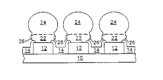
Referring now to Figure 4, solder pads 20 are
reflowed prior to removing the under-bump metallurgy
layer 16 between the contact pads 12, to form an
intermetallic layer 22 at the base of each solder
bump 24. When the topmost component of the under-bump
metallurgy layer is copper (about 1 micron thick) and
conventional lead-tin solder (5 weight percent tin) is
used, the intermetallic 22 which forms is Cu3Sn. It
will be understood by those having skill in the art
that a thin layer of the under-bump metallurgy 16,
typically the bottom chromium layer and the phased
chromium-copper layer (not shown in Figure 4) may
remain on contact pad 12 between the intermetallic
layer 22 and contact pad 12.
~''A
i.
CA 02116766 1998-03-18
'.~,_.
9a
In order to ensure almost complete con~ersion
c_~
,~
,. ~.
CA 02116766 1998-03-18
--10--
metallurgy to the copper/tin intermetallic, reflow
preferably takes place for 1-2 minutes above the
melting point of the solder. The unconverted copper in
the phased chromium-copper region prevents detachment
of the solder bumps from the chromium adhesion layer,
and thereby enhances structural integrity. During
reflow, solder dams 1~ prevent lateral spread and
bridging of the solder and thereby control the size of
the solder bump base. Reflow may be performed in air
or in an inert ambient such as nitrogen, typically with
flux applied, or in a reducing ambient such as
hydrogen, without flux. As is well ~nown to those
having skill in the art, flux residues, if present,
should be cleaned prior to etching the solder dam 18
and the under-bump metallurgy 16.
As also shown in Figure 4, there is a lateral
reaction between the solder 20 and the under-bump
metallurgy 16 during reflow. Accordingly, the
intermetallic layer formed underneath each bump
includes a lip or ridge 26 which typically extends
several microns from the bump. This lip or ridge may
be used to identify solder bumps formed according to
the present invention, because lateral reaction with
the under-bump metallurgy cannot take place if all
under-bump metallurgy between the contact pads is
removed prior to reflow. This lip or ridge 26 also
provides an added degree of protection for the base of
~the solder bump. An improved performance solder bump
is thereby provided.
Referring now to Figure 5, the solder dam 18
and the under-bump metallurgy 16 between the contact
pads 12 are removed, while preserving the base of the
reflowed solder bumps 2~. Since the top copper layer
of the under-bump metallurgy between solder bump 2~ and
contact pad 12 has been converted into an intermetallic
layer, the solder dams and the remaining under-bump
metallurgy between contact pads 12 may be removed,
~, ,
CA 02116766 1998-03-18
--11--
without substantially removing the intermetallic. An
etchant or etchants are used which etch the
intermetallic 22 much more slowly than solder dam 18
and under-bump metallurgy 16. Preferably, the etchants
do not etch the intermetallic 22 while removing solder
dams 18 and intermetallic 22.
For example, for chromium solder dams 18, a
hydrochloric acid based etchant such as Transene CRE473*
is an effective etchant, and a mixture of ammonium
hydroxide and a trace amount of hydrogen peroxide is an
effective copper etchant. Contact to the metal surface
in the substrate with a zinc rod may be required to
initiate etching of chromium. When titanium is used as
a solder dam, a mixture of ammonium hydroxide and
hydrogen peroxide (typically higher peroxide
concentrations than in the copper etchant) is
effective. Multiple etch cycles may be needed to
remove the phased chromium copper layer and the bottom
chromium layer. Neither of these etchants is effective
against the copper/tin intermetallic and neither of
these etchants attacks solder to a detectable extent.
It will be understood by those having skill in the art
that during copper etching, the device may be left in
the etchant for as long as necessary to completely
2S remove the copper between the bumps. It will also be
understood by those having skill in the art that other
etchants may be used, and other removal processes may
~be used.
Accordingly, an improved solder bump
fabrication process is provided. Imperfections in
photolithographic processing of thick film photoresists
also do not degrade alignment. Moreover, undercutting
of the solder bump base during under-bump metallurgy
etching is substantially reduced or eliminated. The
base geometry of the solder bump is therefore
preserved. In fact, the process preferably forms a lip
at the base of the solder bump to further protect the
* trademark
A
CA 02116766 1998-03-18
'_
-12-
solder bump, and enhance electrical and mechanical
reliability. Figure 6 is a scanning electron
microscope photograph of a solder bump formed according
to the present invention, illustrating solder bump 24,
lip 26 and substrate 10.
It will be understood by those having skill
in the art that reduced bump base undercutting may be
obtained with the present invention, independent of
misalignment/distortion reduction, by reflowing the
solder prior to removing the under-bump metallurgy
between the contact pads. For example, in some
microelectronic substrate designs, the designed bump
base may be substantially larger than the contact pads,
so that alignment of the solder bump to the contact
pads is relatively unimportant. Misalignment or
distortion of the solder bump relative to the contact
pads may be tolerated.
A simplified process which allows
misalignment or distortion between the solder bump and
the contact pads will now be described. The under-bump
metallurgy may contain the same bottom chromium layer,
phased chromium/copper layer and top copper layer
described above. However, a second chromium layer is
added on the top copper layer. Solder retaining walls
made, for example, of thick film photoresist, are
formed and patterned as described above. The patterned
solder dam layer described above is not formed.
The second chromium layer is then removed in
the cavities between the solder retaining walls, and
solder is plated as already described. After removing
the solder retaining walls, the solder is reflowed to
form an intermetallic and protect the bump base as
already described. The second chromium layer between
the contact pads prevents the reflowed solder from
,....
,~, ~
CA 02116766 1998-03-18
l,a
bridging. The second chromium layer may be misaligned
relative to the contact pads, but this misalignment may
CA 02116766 1998-03-18
_
-13-
design. The base of the solder bump is still protected
during etching of the under-bump metallurgy by
reflowing prior to removing the under-bump metallurgy
between the contact pads.
In the drawings and specification, there have
been disclosed typical preferred embodiments of the
invention and, although specific terms are employed,
they are used in a generic and descriptive sense only
and not for purposes of limitation, the scope of the
invention being set forth in the following claims.