Note: Descriptions are shown in the official language in which they were submitted.
;~i~u'~~~
SEI 93-44
TITIsE OF THE INVENTION
Pin-Type Dight Receiving Device, Manufacture of the
Pin-Type Light Receiving Device and Optoelectronic
Integrated Circuit
BACKGROUND OF THE INVENTION
Field of the Invention
The present invention relates to a pin-type light
receiving device used in optical fiber communication or
the like, and an optoelectronic integrated circuit in
which the pin-type light receiving device and an
electronic circuit device are monolithically integrated.
Related Background Art
In optical fiber communication or the like, a pin--PD
(Photo Diode) is generally used as a light receiving
device, especially a light receiving device
monolithically integrated together with an electronic
circuit device such as an FET (Field Effect Transistor)
in a optoelectronic integrated circuit. This pin-PD is
mainly formed into a mesa shape from a viewpoint of easy
2(D integration or isolation between devices.
In a conventional pin-PD, for example, an n-type
semiconductor layer, an i-type semiconductor layer, and a
p-type semiconductor layer are sequentially formed on a
semiconductor substrate consisting of InP having
semi-isolation properties, each semiconductor layer is
formed into a mesa shape, and the surface thereof is
1
~; ~. a. ~ 'l J
SE:f 93-44
protected by an insulating layer.
Prior arts about such a mesa type pin-PD are
described in detail in, e.g., "Inst. Phys. Conf., ser.
no. 96, chap. S, Int. Symp. GaAs and Related Compounds,
pp. 571-57~, 1908", "IEEE Photon. Technol. Lett. , vol. 2,
no. 7, pp. 505-506, 1990", and ";Electron. Lett. , vol. 26,
n0. 5, pp. 305--307, 1990°°.
In the above conventional mesa type pin-PD, upon
application of a reverse bias voltage, a depletion layer
extending from the p-type semiconductor layer is exposed
to the surface of the mesa mainly constituted by the
i-type semiconductor layer. P'5ore specifically, the
depletion layer reaches the interface between the side
surface of the i-type semiconductor layer and the
insulating layer for protecting the surface of the i-type
semiconductor layer. For this reasons in accOrdarlCe with
the interface state, a dark current is generated to flow
along the surface of the mesa from the p-type
semiconductor layer to the i-type semiconductor layer.
Therefore, a large amount of dark current is generated.
In addition, in such an optoelectronic integrated
circuit in which a pin-PD and an electronic circuit
device are integrated, when the dark current is
generated, noise is increased to degrade the receiving
sensitivity.
SLTI'~ARY tJF TREE ITTVENTIO1V
2
~~.~.u'~~3
SCI 9:~--~4
The present invention has been made in consideration
of the above problems and has as its object to provide a
pin-type light receiving device which reduces a dark
current to improve device characteristics, a manufacture
of the pin-type light receiving device and an
optoelectronic integrated circW .t in which the pin-type
light receiving device and an electronic circuit device
are integrated to improve the receiving sensitivity.
Tn order to achieve the above object, according to
20 the present invention, there is provided a pin-type light
receiving device comprising a semiconductor substrate, an
n-type semiconductor layer formed on the semiconductor
substrate and doped with an n-type impurity, an n-type
ohmic electrode layer formed on the n-type semiconductor
layer and having an ohmic-contact property, a mesa
portion constructed by an i-type semiconductor layer not
intentionally doped with an impurity and a p-type
semiconductor layer doped ~W th a p-type impurity formed
sequentially on the n-type semiconductor layer and formed
2~ a.nto a mesa shape, and a p-type ohmic electrode layer
formed on the p-type semiconductor layer and having an
ohmic-contact property, wherein a circurnferential border
portion of the p-type semiconductor layer of the mesa
portion is removed to a depth matched substantially a
junction surface between the p-type semiconductor layer
and the i--type semiconductor layer. The depth matched
3
SEI 93-44
substantially the junction surface is set to restrain a
dark current flowing along the surface of the mesa
portion from the p-type semiconductor layer to the i-type
semiconductor layer.
The pin-type light receiving device may further
comprise an etching stop semiconductor layer formed in
contact with the junction surface and having an etching
selectivity different from that of the p°type
semiconductor layer. The p-type semiconductor layer
1G preferably consists of GaInP~s or GaInAsP, and the
etching-stop semiconductor layer preferably consists of
InP. The p-type semiconductor layer preferably consists
of GaInAs or GaInAsP, and the etching stop semiconductor
layer preferably consists of GaInAsP having an energy
band gap Wider than that of GaInAs or GaInAsP
constituting the p-type semiconductor layer.
The e~tcha.ng stop semiconductor layer may further
have an etching selectivity different from that of the i-
type semiconductor layer. The i-type semiconductor layer
20 preferably consists of Galn~s or GaInAsP, and the etching
stop semiconductor layer preferably consists of InP. The
i-type semiconductor layer preferably consists of GaInAs
or GaInAsP, and the etching stop semiconductor layer
preferably consists of-GaTnAsP having an energy band gap
wider than that of GaInAs or GaInllsP constituting the
i-type semiconductor layer.
4
:;;.i~.~'~t~
SEI 93-44
The i-type semiconductor layer may consist of
GaTxl~~s .
In order to achieve the above object, according to
the present invention, there is provided a manufacture of
a pin-type light receiving device comprising a first step
forming sequentially an n-type semiconductor layer doped
with an n-type impurity, an i-type semiconductor layer
not intentionally Japed with an impurity, an etching-stop
semiconductor layer and p-type semiconductor layer doped
2U with a p-type impurity on a semiconductor substrate, a
second step removing a circumferential border portion of
the p-type semiconductor layer to a depth exposed the
etching-stop semiconductor layer to form a first mesa
constituted by the p-type semiconductor layer, a third
step removing sequentially a circumferential border
portion of both the etching-stop semiconductor layer and
the i-type semiconductor layer to form a second mesa
constituted by the etching-sfi:op semiconductor layer and
the i-type semiconductor layer arranged the f first mesa on
24 a center portion of the etching stop semiconductor layer
and a forth step forming an n-type ohmic electrode layer
having an ohmic contact property on the n-'type
semiconductor layer and forming a p-type ohmic electrode
layer having an ohmic contact property on the p-type
semiconductor layer.
In order to achieve the above object, according to
r.~ .~ ~. ~3 ~ ~~
~~I 93-44
the present invention, there is provided an
optoelectronic integrated circuit comprising a pin-type
light receiving device according to the present
invention, and an electronic circuit device electrically
connected to the pin-type light receiving device and
monolithically formed on a semiconductor substrate,
wherein the pin-type light receiving device and the
electronic circuit device are integrated. The electronic
circuit device may be a field effect transistor. The
electronic circuit device may be a bipolar transistor.
In the pin-type light receiving device, the
circumferential border portion of the p-type
semiconductor layer of the mesa portion is removed to the
depth matched the junction surface between the p-type
semiconductor layer and the i-type semiconductor layer,
and the first mesa constituted by the p-type
semiconductor layer and the second mesa constituted by
the i-type semiconductor layer are formed. A depletion
layer extending upon application of a reverse bias
voltage substantially extends through the i-type
semiconductor layer in a direction of thickness from the
p-type semiconductor layer to the n-type semiconductor
layer.
since the diameter of the first mesa is smaller than
that of the second mesa, the depletion layer extending
from the p-type semiconductor layer hardly extends beyond
6
~n ~a
i~J _!~ ~ ~ ~ 2.J v'~
5EI 93-44
the diameter of the first mesa in the radial direction.
For this reason, the depletion layer does not reach the
surface of the second mesa to be exposed. In addition,
since 'the boundary surface between the first and second
mesas matches the junction surface between the p-type
semiconductor layer and the i-type semiconductor layer
and a carrier concentration of the p-type serniconductor
layer is touch higher than that of the i-type
semiconductor layer, the depletion layer extending from
1~ the p-type semiconductor layer hardly extends within the
first mesa in the direction of thickness. For this
reason, the depletion layer does not reach the surface of
the first mesa to be exposed.
Therefore, the depletion layer does not reach the
surfaces of the first and second mesas to be exposed.
That is, the depletion layer does not reach the interface
between the side surface of the i-type semiconductor
layer and the insulating layer for protecting the surface
of the i-type semiconductor layer. As a result, the dark
20 current flowing along the surface of the mesa from the
p-type semiconductor layer to the i-type semiconductor
layer in accordance with the interface state is reduced.
When the etching-stop semiconductor layer is
arranged in contact with the junction surface between 'the
p-type semiconductor layer and the i-type semiconductor
layer, a predetermined etching process for the p-type
7
SEI 93-44
semiconductor layer on the etching stop semiconductor
layer is not continuously performed up to the i-type
semiconductor layer under the etching stop semiconductor
layer. This is because the etching stop semiconductor
layer has an etching selectivity different from that of
the p-type semiconductor layer. For this reason, when
the predetermined etching process for the p-type
semiconductor layer is performec't for the etching stop
semiconductor layer, the etching rate is suppressed or
l~ substantially becomes zero. Therefore, the boundary
surface between the first and second mesas is set with
high reproducibility to almost match the junction surface
between the p-type semiconductor layer and the i-type
semiconductor layer.
At the same time, when the etching stop
semiconductor layer included in the i-type semiconductor
layer is arranged in contact with the junction surface
between the p-type semiconductor layer and the i-type
semiconductor layer, a predetermined etching process for
20 the p-type semiconductor layer on the etching stop
semiconductor layer is not continuously performed for the
i-type semiconductbr layer under the etching stop
semiconductor layer. This is because the etching stop
semiconductor layer has an etching selectivity different
from that of the i-type semiconductor layer and the
p-type semiconductor layer. For this reason, the
rJ ~ ~ ~ '~ C
SEI 93-44
predetermined etching process for the p-type
semiconductor layer is performed for the etching stop
semiconductor layer, the etching rate is suppressed or
substantially becomes zero. Therefore, the boundary
surface between 'the first and second mesas is set with
high reproducibility to almost match 'the junction surface
between the p-type semiconductor layer and the i-type
semiconductor layer.
Further, in the optoelectronic integrated circuit of
~.o the present invention, the pin-type light receiving
device according to the present invention and an
electronic circuit device are monolithically integrated.
In the pin-type light receiving device, the dark current
is reduced. In the electronic circuit device, the noise
input is reduced accordingly to improve the receiving
sensitivity.
The present invention will became more fully
understood from the detailed description given
hereinbelow and the accompanying drawings which are given
20 by way of illustration only, and thus are not to be
considered as limiting the present invention.
Further scope of applicability of the present
invention will become apparent from the detailed
description given hereinafter. I~owever, it should be
understood that the detailed description and specific
examples, while indicating preferred embodiments of the
9
~1.8.~ ~Ji~
s~I 93-~4
invention, are given by way of illustration only, since
various changes and modifications within the spirit and
scope of the invention will become apparent to those
skilled in the art form this detailed description.
DRIFF DESCRIPTION OF THI~ DRAWINGS
Fig. 1 is a sectional view :showing the structure of
the first embodiment of a pin-type light receiving device
according to the present invention;
Fig. 2 is a sectional view showing the structure of a
modification of the pin-type light receiving device in
Fig. 1;
Figs. 3 to fi are sectional views showing s~tpps in the
manufacture of the pin-type light receiving device in
Fig. 1;
Fig. 7 is a schematic view showing the arrangement
of a measurement system for measuring a dark current in
the pin-type light receiving device;
Fig. ~ is a graph showing the relationship between
the diameter of the mesa and the dark current in a general
pin-type light receiving device;
Figs. 9 and 10 are graphs showing the relationship
between the position of the boundary surface between the
mesas with respect to the junction surface between the
semiconductor layers and the dark current value in .the
pin--type light receiving device in Figs. 1 and ~;
Fig. 11 is a sectional view showing the structure of
,, .
_~ 1,~ a :~ ~c
SEI 93-44
the first embodiment of an optoelectronic integrated
circuit according to the present inventiorx;
Fig. 12 is a sectional view showing the structure of
the second embodiment of a pin-type light receiving
device according to the present invention;
Figs. 13 to 17 are sectional views showing steps in
the manufacture of the pin-type light receiving device in
Fig. 12;
Fig. 18 is a graph showing the relationship between
the energy band gap of a GaxnAsP layer and the etching
rate in the pin-type light receiving device in Fig. 12;
Fig. 19 is a sectional view showing the structure of
the second embodiment of an optoelectronic integrated
circuit according to the present invention;
Fag. 20 is a sectional view showing the structure of
the third embodiment of a pin°type light receiving device
according to the present invention;
Figs. 21 to 25 are sectional views showing steps in
the manufacture of the pin°type light receiving device in
Fig. 20; and
Fig. 25 is a sectional view showing the structure of
the third embodiment of an optoelectronic integrated
circuit according to the present invention.
DESC13TPTIO1V OF THE P1WFEFtR~D EMIBODIM~P1TS
The structures and functions of the embodiments
according to the present invention will be described
11
(~~ ~~~~~~e~
s~z 93-44
below with reference to Figs. 1 to 26. In a description
of the drawings, the same reference numerals denote the
same devices, and a detailed description thereof will be
omitted. The sizes in the drawings do not necessarily
accord with those in the description.
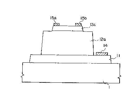
Fig. 1 is a sectional view showing the structure of
the first embodiment of a pin-type light receiving device
according to the present invention. In this pin-type
light receiving device, an n-PD layer 11, an i-PD layer
12a, and a p-PD layer 13c are sequentially formed on a
semiconductor substrate 1. The p-PD layer 13c, the i-PD
layer 12a, and the n-PD layer 11 are sequentially formed
into mesa shapes to respectively constitute the first
mesa, the second mesa, and the third mesa having
truncated conical shapes. ~n n-ohmic electrode layer 1~
is formed on 'the n-PD layer 11 at a predetermined
position. P-ohmic electrode layers 15a and 15b are
formed on the p-PD layer 13c at predetermined positions.
A passivation layer (not shown) is formed on the surface
of each mesa.
The. semiconductor substrate 1 consists of InP doped
with Fe at a predetermined dopant concentration and has
semi-isolation properties. The n-PD layer 11 consists of
InP doped with ~i at a dopant concentration of about 2 ~
108 ctri 3 and has a thicl~ness of about 300 to 500 nm and the
n conductivity type. The i-PD layer 12a consists of
12
.iL .~. ~J ~)
~~ ~ 2! t~
SEI 93-44
GaInAs or GaInAsP not intentionally doped with a dopant
(at a dopant concentration of about 1 x lOls to 2 ~ 1015
cm"3) and has a thickness of about 2.0 to 2.5 ~m and a high
resistivity. The p-PD layer 13c consists of GaInAs or
GaInAsP doped with Zn at a dopant concentration of about 1
~c 1018 can 3 and has a thickness of about 100 nm and the p
conductivity type.
The first mesa mainly constituted by the p-PD layer
13c has a diameter of. about 100 ~,m. The second mesa
mainly constituted by the i-PD layer 12a has a diameter of
about 120 Vim. The third mesa mainly constituted by the
n-PD layer 11 has a diameter of about 1~0 to 150 psm. The
n-ohmic electrode layer 1~~ consists of AuGe/Ni and has a
good ohmic-contact property with respect to the n-PD
layer 11. The p-ohmic electrode layers 15a and 15b
consist of Ti/Pt/Au and have a good ohmic-contact
property with respect to the p-PD layer 13c. The
passivation layer (not shown) consists of SiN and has
isulation properties.
The diameter of the first mesa is formed smaller
than that. of the second mesa. The boundary surface
between the f first and second mesas is formed to match the
junction surface between the p-PD layer 13c and the i-PD
layer 12a. Because of 'the problem of precision in the
manufacturing process, the boundary surface between the
first and second mesas is actually formed to be arranged
13
;3
SEI 93-44
near the lower side of the junction surface between the
p-PD layer 13c and the i-PD layer 12a. For this reason,
the first mesa is mainly constituted by the p-PD layer 13c
and includes part of the i-PD layer 12a. The second mesa
is constituted by the remaining part of the i-PD layer 12a
which is not included in the fir st mesa.
The function of the pin-type light receiving device
according to the first embodiment will be described
below.
In this pin-type light receiving device, the first
mesa mainly constituted by the p-PD layer 13c and the
second mesa mainly constituted by the i-PD layer 12a are
formed. A depletion layer extending upon application of
a reverse bias voltage substantially extends through the
i-PD layer 12a in the direction of thic3cness from the p-PD
layer 13c to the n-PD layer 11.
Since the diameter of the first mesa is smaller than
that ~f the second mesa., the depletion layer extending
from the p-PD layer 13c does not extend beyond the
diameter of the first mesa in the radial direction. For
this reason, the depletion layer does not reach the
- surface of the second mesa to be exposed. Since the
boundary surface between the first and second mesas
matches the junction surface between the p-PD layer 13c
and the i-PD 7.ay~r 12a and a carrier concentration of the
p-PD layer 13c is much higher than that of the i-PD layer
14
~~ ')
~~w ~ 9 .:~ ,°.j
SEI ~3-44
12a, the depletion layer extending from the p-PD layer
13c hardly extends within the first mesa in the direction
of thickness . For this reason, t:he depletion layer does
not reach the surface of the fir:>t mesa to be exposed.
Therefore, the depletion layer does not reach the
surfaces of the first and second mesas to be exposed.
That is, the depletion layer doer not reach the interface
between the side surface of the i-PD layer 12a and the
passivation layer knot shown) for protecting the surface
of the i-PD layer 12a. As a result, the dark curxent
flowing along the surface of the mesa from the p-PD layer
13c to the i-PD layer 12a in accordance with the interface
state is reduced.
Fig. 2 is a sectional view showing the structure o~ a
modification of the pin-type light receiving device
according to the first embodiment. The pin-type light
receiving device has almost the same structure as in the
first embodiment. Almost as in the first embodiment, the
diameter of the first mesa is formed smaller than that of
the second mesa. The boundary surface between the first
and second mesas is formed to match the junction surface
between the p-PD layer 13c and the i-PD layer 12a.
However, this modification is different from the
first embodiment in that the boundary surface between the
first and second' mesas is actually formed to be arranged
near the upper side of the junction surface between the
~l
~_ ~_ z~ ~ ~ -
;,
SEI 93-~4
p-PD layer 1.3c and the i-PD layer 12a because of the
problem of precision in the manufacturing process. For
this reason, the second mesa is mainly constituted by the
i-PD layer 9.2a and includes part of the p-PD layer 13c.
The first mesa is constituted by the remaining part of the
p-PD layer 13c which is not included in the second mesa.
With the above structure of the pin-type light
receiving device, almost the same operation as in the
first embodiment can be performed.
la Steps in the manufacture of the first embodiment of
the pin-type light receiving device will be described
below. Figs. 3 and 4 are sectional views showing the
steps in the man~zfacture of the first embodiment of 'the
pin-type light receiving device.
By conventional OI~vPE (~rganometallic vapor Phase
Epitaxy) method, the n-PD layer 11, the i-PD layer 12a,
and the p-PD layer 13c are sequentially formed on the
semiconductor substrate 1. (~°ig. 3) .
By conventional photolithography technique, the
20 first mask pattern having a predetermined circular shape
is formed on the p-PD layer 13c. The p-PD layer 13c is
formed into a mesa shape by conventional wet etching
method using a phosphoric acid (I33PO4) etching solution to
form the first mesa. In this case, the etching rate for
the p-PD layer 13c is measured beforehand. By measuring
the etching tame on the basis of this etching rate, the
16
~~. i~ ~J~'~
SET 93-44
etching depth is controlled to be matched to the
thickness of the p-PD layer 13c. By conventional
photolithography technique, the second mask pattern
having a predetermined circular shape is formed on the
p-PD layer 13c and the i-PD layer 12a . The i-PD layer 12a
is formed into a mesa shape by conventional wet etching
using a phosphoric acid etching solution to form the
second mesa. Tn this case, the diameter of the second
mask pattern is larger than that of the first mask
pattern. Since the etching selectivity of the i.-PD layer
12a is different from that of the n-PD layer 11, when the
etching depth reaches the surface of 'the n-PD layer 11,
the etching for the i-PD layer 12a is stopped ( Pig. 4 ) .
By conventional photolithography technique, the
third mask pattern having a predetermined circular shape
is formed on the n-PD layer 11. The n-PD layer 11 is
formed into a mesa shape by conventional wet etching
using a hydrochloric acid (HC1)' etching solution to form
the third mesa (fig. 5).
2Q Subsequently, by conventional plasma CvD (Chemical
Vapor Deposition) method, a passivation layer (not shown)
is deposited on the n-PD layer 11, the i-PD layer 12a, and
the p-PD layer 13c. By conventional RIE (Reactive Ton
Etching) method, the passivation layer on the n-PD layer
11 and the p-PD layer 13c is removed at predetermined
positions to :Form openings for forming electrodes. By
17
.d. ~. U ~e :i
SEI 93-44
conventional vacuum deposition method, the n-ohmic
electrode layer 14 is deposited in the opening on the n-PD
layer 11, and the p-ohmic electrode layers 15a and 15b are
deposited in the openings on the p-PD layer 13c (Fig. 6) .
An experiment about 'the pire-type light receiving
device of the first embodiment will be described below.
Fig. 7 is a schematic view showing the arrangement of the
measurement system for measuring a dark. current in the
pin-type light receiving device.
A dark box 30 and an instrument 31 were arranged in
the measurement system. A pin-type light receiving
device was placed in the dark box 30 as a target object
for the dark current measurement. A coaxial cable 32a was
connected to one terminal of the instrument 31, and a
coaxial cable 32b was connected to the other terminal. A
probe 33a connected to the distal end of the coaxial cable
32a was brought into contact with the p-ohmic electrode
layer of the pin-type light receiving device. A probe 33b
connected to the distal end of the coaxial cable 32b was
brought into contact with the n-ohmic electrode layer of
the pin-type light receiving device.
A~ the dark box 30, a box covered with a cover having
a black inner surface and shielding the external light
was used. As the instrument 31, a semiconductor
parameter analyzer (414513 available from YHP) was used.
As an experiment condition, the environment temperature
18
w.~~.~'l ~3
SEA 93-44
was set to be about 300 K.
Fig. 8 is a graph showing the relationship between
the diameter of the mesa and the dark current value in a
general pan-type light receiving device. The diameter of
the mesa constituted by a p-type semiconductor layer and
an i-type semiconductor layer i~~ plotted in logarithm
along the abscissa. The value of the generated dark
current is plotted in logarithm along the ordinate.
The measurement result of a verification experiment
is shown in Fig. 8. The experiment iaas performed by
measuring tine dark current in the general pin-type light
receiving device by using the measurement system shown in
Fag. 7 while the diameter of the mesa constituted by the
p-type semiconductor layer and the i-type semiconductor
layer was variously set. As an experiment condition, the
environment temperature was set to be about 300 K.
As shown in Fig. ~, as the diameter of the mesa
increases, the dark current tends to increase. More
specifically, when the diameter of the mesa is about 100
dam, the amount of generated dark current has a linearity
depending on 'the first power of the diameter of the mesa.
When the diameter of the mesa is about 1 mm or more, the
amount of generated dark current substantially has a .
linearity depending on the second power of the diameter
of the mesa. As a result, it is assumed that the dark
current flowing in the interface between the side surface
19
.~.~u ~~)~
SEI 93-44
of the mesa and the passivation :Layer for protecting the
surface of the mesa in accordance with the interface
state greatly contributes to the measured dark current.
Figs . 9 and 10 are graphs each showing the
relationship between the position of the boundary surface
between the mesas with respect to the junction surface
between the semiconductor layers and the dark current
value in the first embodiment of the pin-type light
receiving device. The origin of the abscissa is set to
1Q the position of the junction surface between the p-PD
layer 13c and the i-PD layer 12a. The distance from the
junction surface to the boundary surface between the
first mesa mainly constituted by the p-PD layer 13c and
the second mesa mainly constituted by the i-PI3 layer 12a
is ~alotted along the abscissa. The direction from the
semiconductor substrate 1 to the junction surface is set
to be a negative direction. The value of the generated
dark current is plotted in logarithm along the ordinate.
The measurement result of an initial experiment is
2~ shown in Fig. 9. The experiment was performed by
measuring the dark current in the first embodiment of the
pin-type light receiving device by using the measurement
system shown in Fig, 7 while the interval between the
junction surface of the semiconductor layers and the
boundary surface between the mesas is variously set, The
measurement result of a reproduction experiment is shown
.~~..1.l~~~~a
SEI 93-44
in Fig. 10. The reproduction experiment was performed to
confirm the measurement result shown in Fig. 9. As the
conditions for these two experiments, 'the diameter of the
first mesa was constantly set to be about 100 ~m and the
environment temperature was set to be about 300 K. In the
reproduction experiment, no pin-type light receiving
device having values in the negative direction of the
abscissa was used as the target object for the
measurement. Therefore, for the sake of comparison with
the initial experiment, one of solid curves in Fig. 9 is
indicated by a dotted curve in Fig, 10.
As shown in Figs. 9 and 10, the measurement results
in these two experiments exhibit almost the same tendency
that as the boundary surface between the first and second
mesas is close to the junction surface between the p-PD
layer 1~c and the i-PD layer 12a, the generated dark
current is reduced. As a result, it is assumed that in
order to reduce the dark current to a practical level of
several tens nA or less, the boundary surface between the
first and second mesas need to be separated from the
junction surface between the p-PD layer 13c and the i-PD
layer 1.2a at an interval of about 25 to 50 nm or less.
Fig. 11 is a sectional view showing the structure of
the first embodiment of an optoelectronic integrated
circuit accorriing to the present invention. A pin-PD 10a
and a HEMT (Hi.gh Electron Mobility Transistor) 20 are
21
rd a
SEI 93-44
monolithically integrated on the: semiconductor substrate
1. In this optoelectronic integrated circuit, a buffer
layer 21, a channel layer 22, a electron supply layer 23,
an n-PD layer 11, an i-PD layer 12a, and a p-PD layer 13c
are sequentially formed on a semiconductor substrate 1.
In the pin-PD 10a, the p-PD layer 13c, the i--PD layer
12a, and the n-PD layer 11 are sequentially formed into
mesa shapes to respectively constitute the first mesa,
the second mesa, and the third mesa having truncated
conical shapes . The n-ohmic electrode layer 14 is formed
on the n-PD layer 11 at a predetermined position. The
p-ohmic electrode layers 15a and 15b ire formed on the
p-PD layer 13c at predetermined positions. The pin-PD
1~a has the same structure as the pin-type light
receiving device of the first embodiment.
In the I~EI~IT 2~0, the p-PD layer 13c, the i-PD layer
12a, and the n-PD layer 11 are sequentially removed, and
the electron supply layer 23, the channel layer 22, and
the buffer layer 23. are formed to be separated from the
region of the pin-PD loa. A gate electrode layer 24 and
ohmic electrode layers 25a and 25b are formed on the
electron supply layer 23 at predetermined positions. A
region where the gate electrode layer 24 is formed on the
electron supply layer 23 has a recess structure having a
recessed portion with a predetermined depth. The device
characteristics such as a threshold voltage are
22
C iy
SEI 93-44
controlled in accordance with the depth of the recessed
portion.
A passivation layer 2 is formed on the surface of
each semiconductor layer of the pin-PD 10a and the HEMP
20. A wiring layer 3 is formed between the n-ohmic
electrode layer 1~ of the pin-PD 10a and the ohmic
electrode layer 25a of the HEMT 20. A wiring layer 4 is
formed between the p-ohmic electrode layer 15a of the
pin-PD 10a and the electrode layer of an adjacent device
(not shown) . A wiring layer 5 is formed between the ohmic
electrode layer 25b of the HEMT 20 and the electrode layer
of an adjacent device knot shown) .
The buffer layer 21 consists of InP not
intentionally doped with a dopant and has a thickness of
about 200 to 300 nm. The channel layer 22 consists of
GaInAs not intentionally doped with a dopant and has a
thickness of 50 to 100 nm. The electron supply layer 23
consists of AlIaaAs doped with Si at a dopant
concentration of about 5 x 101' to 1 x 10'8 cm 3 and has a
thickness of about 1.00 to 150 nm and the n conductivity
type. The gate electrode layer 24 consists of Ti/Pt/Au
and has a good Schottky-contact property with respect to
the electron supply layer 23. The ohmic electrode layers
25a and 25b consist of AuGe/Ni and have a good
ohmic-contact property with respect to the electron
supply layer ;Z3. The passivation layer 2 consists of SiN
23
N~J ~ ~ ~~ '~ ~,' CJ
S~z 93-~4
and has isolation properties. The wiring layers 3 to 5
consist of A1 and electrically connect the adjacent
devices.
The diameter of the first mesa is formed smaller
than that of the second mesa. The boundary surface
between the f first and second mesas is formed to match the
aunction surface between the p-PD layer 13c and the i-PD
layer 12a.
The function of the optoelectronic integrated
circuit of the first embodiment will be described below.
In this optoelectronic integrated circuit, the
pin-PD 10a and the ~~iT 20 are monolithically integrated
on the semiconductor substrate 1. In the pin°PD 10a, a
depletion layer extending upon application of a reverse
bias voltage substantially extends through the i-PD layer
12a in the direction of thickness from the p-PD layer 13c
to the n-PD layer 11. As in the pin~type light receiving
device of the first embodiment, since the diameter of the
first mesa is smaller than that of the second mesa, and
the boundary surface between the first and second mesas
matches the junction surface between the p-PD layer 13c
and the i-PD layer 12a, the depletion layer extending
upon application of the reverse bias voltage does not
reach the sur:~aces of the first and second mesas to be
exposed. That is, the depletion layer does not reach the
interface between the side surface of the i-PD layer and
24
SET 93-44
the passivation layer 2.
For this reason, the dark current f lowing along the
surface of the mesa from the p-PD layer 13c to the i-PD
Layer 12a in accordance with the interface state is
reduced. Therefore, in the HEINIT 20, a noise signal input
to the ohmic electrode layer 25a through the wiring layer
3 is reduced to improve the receiving sensitivity to the
light signal received by the pan-PD 10a.
Fig. 12 is a sectional view showing the structure of
the second embodiment of a pin-type light receiving
device according to the present invewtion. In this
pin-type light receiving device, an n-PD layer 11, an
i-PD layer 12a, a p-PD layer 13a, an etching stop layer
13b, and a p-PD layer 13c are sequentially formed on a
semiconductor substrate 1. The p-PD layer 13c is formed
into a mesa shape to constitute the first mesa having a
truncated conical shape. The etching stop layer 13b, the
p-PD layer 13a, and the i-PD layer 12a are formed into a
mesa shape to constitute the second mesa having a
truncated conical shape. The n-PD layer 11 is formed into
a mesa shape to constitute the third mesa having a
truncated conical shape. An n-ohmic electrode layer 14
is formed on the n-PD layer 11 at a predetermined
position. P-ohmic electrode layers 15a and 15b are
formed on the p-PD layer 13c at predetermined positions.
A passivation layer (not shown) is formed on the surface
f~
I .tS_ ..~ L~ ~ ~ eJ' C
SEI 93-44
of each mesa.
The semiconductor substrate 1 consists of InP doped
with Fe at a predetermined dopant concentration and has
semi-isulation properties. The n-PD layer 11 consists of
InP doped with Si at a dopant concentration of about 2 x
1018 c~ 3 and has a thickness of about 300 to 500 nm and the
n conductivity type. The i-PD layer 12a consists of
GaInAs or GaInAsP not intentionally doped with a dopant
( at a dopant concentration of about 1 x 10¹⁵ to 2 x 10¹⁸
cry 9) and has a thickness of about 2.0 to 2.5 dam and a high
resistivity. The p-PD layer 13a consists of GaInAs or
GaInAsP doped with Zn at a dopant concentration of about 1
x 1019 can 3 and has a thickness of about 5 to 10 nm and the p
conductivity type: The etching stop layer 13b consists
of InP or GaInAsP doped with ~n at a dopant concentration
of about 5 X 101 Cmy3 and ~'laS a thickness of about 5 to 10
nm and the p conductivity type. The p-PD layer 13c
consists of GaInAs or GaInAsP doped with 2n at a dopant
concentration of about 1 x 10¹⁸ c~ 3 and teas a thickness of
about 100 nm and the p conductivity type.
The ,first mesa mainly constituted by the p-PD layer
13c has a diameter of about 100 ~,m. The second mesa
mainly constituted by the i-PD layer 12a has a diameter of
about 120 plm. The 'third mesa mainly constituted by the
n-PD layer 11 has a diameter of about 140 to 150 ~Sm. The
n-ohmic electrode layer 14 consists of AuGe/Ni and has a
26
0
;,,.~~_b~r~~
SEI 93-4~
good ohmic-contact property with respect to the n-PD
layer 11. The p-ohmic electrode layers 15a and 15b
consist of Ti/Pt/.Au and have a good ohmic contact with
respect to the p-PD layer 13c. '.Phe passivation layer (not
shown) consists of SiN and has isulation properties.
The diameter of the first mesa is formed smaller
than that of the second mesa. The boundary surface
between the first and second mesas is farmed to match the
junction surface between the p-PD layer 13c and the
etching stop layer 13b.
When the etching stop layer 13b consisting of
GaInAsP is used with respect to the p-PD layer 13c
consisting of GaInAs or GaInAsP, the etching
selectivities for a phosphoric acid etching solution in
these two semiconductor layers change in accordance with
the energy band gap, i.e., the composition ratio of
GaInAsP. For this reason, the composition ratio of
~aInAsP must be considered in advance. Thus, GaIn.AsP
constituting the etching stop layer 13b must have an
energy band gap wider than that of GaInAs or GaInAsP
constitwting the p-PD layer 13c.
When the etching stop layer 13b consisting of InP is
used with xespect to the p-PD layer 13c consisting of
walrus, the etching selectivities for a phosphoric acid
etching solution in these two semiconductor layers are
campletely different from each other.
27
~ ~r~~~
- SEI 93-4~
When the etching stop layer 13b consisting of IriP i.s
used with respect to the p-PD layer 13c consisting of
GaInAsP, the etching selectivities for a phosphoric acid
etching solution in these two semiconductor layers change
in accordance with the energy band gap, i.e., the
composition ratio of GaInAsP. For this reason, the
composition ratio of GaInAsP must be considered in
advance. Thus, GaInAsP constituting the p-PD layer 13c
must have an energy band gap narrower than that of InP
1o constituting the etching stop layer 13b.
When the etching stop layer 13b is formed directly
on the i-PD layer 12a without forming the p-PD layer 13a,
the hetero junction between the i-PD layer 12a and the
etching stop layer 13b may cause an increase in dark
current depending on its quality. Therefore, the quality
of the heterojunction must be considered in advance.
The function of the second embodiment of the
pin-type light receiving device will be described below.
In this pin-type light receiving device, the first
20 mesa mainly constituted by the p-PD layer 13c and the
second mesa anainly constituted by the i-PD layer 12a are
formed: A depletion layer extending upon application of
a reverse bias voltage substantially extends 'through the
i-PD layer 12a in a direction of thickness from the p-PD
layer 13c to the n-PD layer 11.
Since the etching stop layer 13b and the p-PD layer
28
Y
SE:L 93-44
13a are very thin, and the diameter of the first mesa is
smaller than that of the second mesa, the depletion layer
extending from the p-PD layer 13c hardly extends beyond
the diameter of the first mesa in a radial direction. For
this reason, the depletion layea: does not reach the
surface of the second mesa to be exposed. Since the
boundary surface between the first and second mesas
matches the junction surface between the p-PD layer 13c
and the etching stop layer 13b and a carrier
concentration of the p-PD layer 13c is much higher than
that of the i-PD layer lea, the depletion layer extending
from the p-PD layer 13c hardly extends within the first
mesa in the direction of thickness. For this reason, the
depletion layer does not reach the surface of the first
mesa to be exposed.
The etching stop layer 13b is formed between the
p-PD layer 13c and the p-PD layer 13a and has an etching
selectivity different 'from that of~ the p-PD layer 13c.
For this reason, even when the etching process for the
2~ p-PD layer 13c is continuously performed to the etching
stop layer 13b, the etching rate is suppressed or
substaiatially becomes zero. Thus, the boundary surface
between the first and second mesas is set with high
reproducibility to almost match the junction surface
between the p-PD layer 13c and the etching stop layer 13b.
Therefore, the depletion layer does not reach the
29
;~1_~.~~~'
SEI 93-44
surfaces of the first and second mesas to be exposed.
That is, the depletion layer does not reach, the interface
between the side surface of the i-PD layer 12a and the
passivation layer (not shown) for protecting the surface
of the i-PD layer 12a. As a result, the dark current
flowing along the surface of the mesa from the p-PD layer
13c to the i-PD layer 12a in accordance with the interface
state is reduced.
steps in the manufacture of the second embodiment of
the pin-type light receiving device will be described
below. Figs. 13 to 17 are sectional views showing the
steps in the manufacture of the second embodiment of the
pin-type light receiving device.
By conventional DMVPF method, the n-PD layer 11, the
i-PD layer 12a, the p-PD layer 13a, the etching stop layer
13b, and the p-PD layer 13c are sequentially formed on the
semiconductor substrate 1 (Fig. 13).
Dy conventional photolithography technique, the
first mask pattern having a predetermined circular shape
is farmed on the p-PD layer 13c. The p-PD layer 13c is
formed into a mesa shape by conventional wet etching
method 'using a phosphoric acid etching solution to form
the first mesa. since the p-PD layer 13c has an etching
selectivity different from that of the etching stop layer
13b, when the etching depth reaches the surface of
etching stop layer 13b, etching for the p-PD layer 13c is
SEI 93-44
stopped (Pig. 14).
By conventional photolithography technique, the
second mask pattern having a predetermined circular shape
is formed on the p-PD layer 13c and the etching stop layer
13b. The etching stop layer 13b is formed into a mesa
shape by conventional wet etching using a hydrochloric
acid etching solution. Subsequently, the p-PD layer 13a
and the i-PD layer 12a are formed into a mesa shape by
conventional wet etching using a phosphoric acid etching
solution to form the second mesa. Since the i-PD layer
12a has an etching selectivity different from that of the
n-PD layer 11, when the etching depth reaches the surface
of the n-PD layer 11, etching for the p-PD layer 13a and
the p-PD layer 12a is stopped. The diameter of the second
mask pattern is larger than that of the first mask pattern
(Fig. 15).
By conventional photolithography technique, the
third mask pattern having a predetermined circular shape
is formed on the n-PD layer 11. The n-PD layer 11 is
20, formed into a mesa shape by conventional wet etching
using a hydrochloric acid etching solution to form the
third mesa (Fig. 16) .
Subsequently, by conventional plasma CVD method, a
passivation layer (not shown) is deposited on the n-PD
layer 11, the i-PD layer 12a, and the p-PD layer 13c. By
conventional RTE, the passivation layer on the n-PD layer
31
~.~.~~'~~~3
SEI 93-44
11 and the p-PD layer 13c is removed from predetermined
positions to form openings for forming electrodes. By
conventional vacuum deposition method, the n-ohmic
electrode layer 14 is deposited in the opening on the n-PD
layer 11, and the p-ohmic electrode layers 15a and 15b are
deposited an the openings on the p-PD layer 13c (Fig. 17) .
An experiment about the pin-type light receiving
device of the second embodiment will be described below.
Fig. 1~ is a graph showing the relationship between the
energy band gap of the GaInAsP layer and the etching rate
in the pin-type light receiving device of the second
embodiment. The energy band gap of GaIn~.sP constituting
the etching stop layer 13b is plotted along the abscissa.
The etching rate in etching of GaInAsP using a phosphoric
acid etching solution is plotted along the ordinate. The
measurement values represented by hollow dots were
obtained by using GaInAsP having an energy band gap
lattice-matched with InP as~ a target object for
measurement. The component volume ratio of the etching
solution was H3POa : H202 : Fi20 d 5 : 1 : 40.
As shown in Fig. 18, as the energy band gap of
GaInAsP is increased, the etching rate in etching of
GaInAsP using a phosphoric acid solution tends to
decrease. When the etching stop layer 13b consisting of
Galn.~sP is used with respect to the p-PD layer 13c
consisting of GaInAs or GaInAsP, the etching
32
~.~ .~ '' ui
SEI 93-44
selectivities for a phosphoric acid etching solution in
these two semiconductor layers change in accordance 'with
the energy band gap, i.e., the composition ratio of
GaTnAsP. Tn this case, the energy band gap of GaInAs is
about 0.75 eV. Therefore, when the p-PD layer 13c is
formed of GaInAs, the energy band gap of GaInAs
constituting the etching stop layer 13b must be 0.75 ev or
more. When the p-PD layer 13c is formed of GaInAsP,
GaInAsP constituting the etching stop layer 13b must have
an energy band gap wider than that of GaInAsP
constituting the p-PD layer 13c.
When the etching stop layer 13b consisting of InP is
used with respect to the p-PD layer 13c consisting of
GaInAs, the etching selectivities for a phosphoric acid
etching solution in these two semiconductor layers are
completely different from each other. This is because
the energy band gaps of GaInAs and InP are about 0.75 ev
and about 1.35 ev, respectively, to exhibit a
sufficiently large difference.
When the etching stop layer 13b consisting of InP is
used with respect to the p-PD layer 13c consisting of
GaInAsP, the etching selectivities for a phosphoric acid
etching solution in these two semiconductor layers change
in accordance with the energy band gap, i . a . , the
composition ratio of GaInAsP. In this case, the energy
band gap of In:P is about 1.35 ev. Therefore, the energy
33
~~u.~3~~~~
SEI 93-44
band gap of GaTnAsP constituting the p-PD layer 13c rniast
be about 1.35 e'U or less.
Fig. 19 is a sectional view showing the structure of
the second embodiment of an optoelectronic integrated
circuit according to the present invention. A pin-PD 10b
and a HEMT 20 are monolithically integrated on the
semiconductor substrate 1. In this optoelectronic
integrated circuit, a buffer layer 21, channel layer 22,
an electron supply layer 23, an n-PD layer 11, an i-PD
layer 12a, a p-PD layer 13a, an etching stop layer 13b,
and a p-PD layer 13c are sequentially formed on the
semiconductor substrate 1.
Tn the pin-PD 10b, the p-PD layer 13c is formed inter
a mesa shape to constitute the first mesa having a
truncated conical shape. The etching stop layer 13b, the
p-PD layer 13a, and the i-PD layer 12a are formed into a
mesa shape to constitute the second mesa having a
truncated conical shape. The n-PD layer 11 is formed into
a mesa shape to constitute the third mesa having a
truncated conical shape. The n-ohmic electrode layer 14
is formed on the n-PD layer 11 at a predetermined
position. The p-ohmic electrode layers 15a and 15b are
i~ormed on the p-PD layer 13c at predetermined positions.
The pin-PD 10b has the same structure as the second
embodiment of the pin-type light receiving device.
In the IiEMT 20, the p-PD layer 13c, the etching stop
34
SEI 93-44
layer 13b, the p-PD layer 13a, the i-PD layer 12a, and. the
n-PD layer 11 are sequentially removed. The electron
supply layer 23, the channel layer 22, and the buffer
layer 21 are separated from the region of the pin-PD 10b.
A gate electrode layer 24 and ohmic electrode layers 25a
and 25b are formed on the electron supply layer 23 at
predetermined positions. A region where the gate
electrode layer 24 is f~rmed on the electron supply layer
23 has a recess structure having a recessed portion with a
predetermined depth. The device characteristics such as
a threshold voltage are controlled in accordance with the
depth of the recessed portion. The HEMT 20 has the same
structure as the first embodiment of the optoelectronic
integrated circuit.
A passivation layer 2 is formed on the surface of
each semiconductor layer of the pin-PD 10b and the HEMT
20. A wiring layer 3 is formed between the n-ohmic
electrode layer 14 of the pin-~D 10b and the ohmic
electrode layer 25a of the I3EMT 20. A wiring layer 4 is
29 formed between the p-ohmic electrode layer 15a of the
pin°PD 10b and the electrode layer of an adjacent device
(not shown) . A wiring layer 5 is formed between the ohmic
electrode layer 25b of the HEMT 20 and the electrode layer
of an adjacent device (not shown) .
The diameter of the first mesa is formed smaller
than that of the second mesa. The boundary surface
:~.~~u ~~~3
~SEI 93-~4
between the first and second mesas is formed to match the
junction surface between the p-PD layer 13c and the
etching stop layer 13b.
The function of the second embodiment of the
optoelectronic integrated circuit will be described
below.
Tn this optoelectronic integrated circuit, the
pin-PD 10b and the HEMT 20 are monolithically integrated
on the semiconductor substrate 1. In the pin-PD 10b, a
depletion layer extending upon application of a reverse
bias voltage substantially extends through the i-PD layer
12a in the direction of thickness from the p-PD layer 13c
to the n-PD layer 11. As in the. pin-type light receiving
element of the second embodiment, since the diameter of
the .first mesa is smaller than that of the second mesa,
and the boundary surface between the f first and second
mesas matches the junction surface between the p-PD layer
13c and the etching stop layer 13b, the depletion layer
extending upon application of the reverse bias voltage
2~ does not reach the surfaces of the first and second mesas
to be exposed. That is, the depletion layer does not
reach the interface between the side surface of the i-PD
layer 12a and the passivation layer 2.
The etching stop layer 13b is formed between the
p-PD layer 13c and the p-PD layer 13a and has an etching
selectivity different from that of the p-PD layer 13c.
36
j~~~'~~~
SE I 9 3-44
For this reason, even when the etching process for the
p-PD layer 13c is continuously performed for the etching
stop layer 13b, the etching rate is suppressed or
substantially becomes aero. Thus, the boundary surface
between the f first and second mesas is set with. high
reproducibility to almost match the junction surface
between the p-PD layer 13c and the etching stop layer 13b.
The dark current flowing along the surface of the
mesa from the p-PD layer 13c to the i-PD layer 12a in
accordance with the interface state is reduced.
Therefore, in the HEMT 20, a noise signal input to the
c~hmic electrode layer 25a through the wiring layer 2 is
decreased to improve the receiving sensitivity to the
light signal received by the pin-PD 10b.
Fig. 20 is a sectional view showing the structure of
the third embodiment of a pin-type light receiving device
according to the present invention. In this pin-type
light receiving device, an n-PD layer 11, an i-PD layer
12a, an etching stop layer 12b, an i-PD layer 12c, and a
p-PD layer 13c are sequentially formed on a semiconductor
substrate 1. The p-PD layer 13c and the i-PD layer 12c
are fox°med into a mesa shape to constitute the first mesa
having a truncated conical shape. The etching stop layer
12b and the i-PD layer 12a are formed into a mesa shape t~
constitute the secand mesa having a truncated conical
shape. The n-~PD layer 11 is formed into a mesa shape to
37
'.~ .1~ ..~. ~ ~~ v~ c9
SEI 93-4~
constitute the third mesa having a truncated conical
shape. An n-ohmic electrode layer 1~ is formed on the
n-PD layer 11 at a predetermined position. P-ohmic
electrode layers 15a and 15b are formed on the p-PD layer
13c at predetermined positions. A passivation layer (not
shown) is formed on the surface of each mesa.
The semiconductor substrate 1 consists of InP doped
with ~°e at a predetermined dopant concentration and has
semi-isolation properties. The n-PD layer 11 consists of
InP doped with Si at a dopant concentratioza of about 2 x
101a cm 3 and has a thickness of about 300 to 500 nm and the
n conductivity type, The i-PD layer 12a consists of
GaIxaAs or GaInAsP not intentionally doped with a dopant
at a dopant concentration of about 1 x 10¹⁵ to 2 x 10¹⁵
cm 3) and has a thickness of about 2.0 to 2.5 ~m and a high
resistivity. The etching stop layer 12b consists of InP
or GaInAsP not intentionally doped with a dopant and has a
thickness of about 5 to 10 nm and a high resistivity. The
i°-PD layer 12c consists of GaInAs pr GaIrzAsP not
intentionally doped with a dopant and has a thickness of
about 5 to 10 nm and a high resistivity. The p--PD layer
13c consists of GaInAs or GaInAsP doped with Zn at a
dopant concentration of about 5 x 10¹⁸ cap 3 and has a
thickness of about 100 nm and the p conductivity type.
The first mesa mainly constituted by the p-PD layer
13c lass a da.arneter of about 100 ~.m, The second mesa
38
r,~ ~_ ~. ~3 ,~~
SEI 93-44
mainly constituted by the i-PD layer 12a has a diameter of
about 120 Vim. The third mesa mainly constituted by the
n-PD layer 11 has a diameter of about 140 to 150 Vim. The
n-ohmic electrode layer 14 consists of AuGe/Ni and has a
good ohmic-contact property with respect to the n-PD
layex 11. T'he p-ohmic electrode layers 15a and 15b
consist of Ti/Pt/Au and has a good ohmic-contact property
with respect to the p-PD layer 13c. The passivation layer
(not shown) consists of SiN and has isulation properties.
1~0 The diameter of the first mesa is formed smaller
than that of the second mesa. The boundary surface
between the first and second mesas is formed to match the
junction surface between the i-PD layer 12c and the
etching stop layer 12b.
When the etching stap layer 12b consisting of
GaInAsP is used with respect to the i-PD layer 12c
consisting of GaInAs or GaInAsP, the etching
selectivit~.es for a phosphoric acid etching solution in
these two semiconductor layers change in accordance with
20 the energy band gap, i.e., the composition ratio of
GaInAsP., For this reason, the composition ratio of
GaInAsP must be considered in advance. Thus, GaInAsP
constitwting the etching stop layer 12b must have an
energy band gap wider than that of GaInAs or GaInAsP
constituting the i-PD layer 12c.
When the etching stop layer 12b consisting of InP is
39
.;
s~z g3°~4
used with respect to the i-PD layer 12c consisting of
GaInAs, the etching selectivities for a phosphoric acid
etching solution in these two semiconductor layers are
completely different from each other.
When the etching stop layer 12b consisting of InP is
used with respect to the i-PD layer 12c consisting of
GainAsP, the etching selectivities for a phosphoric acid
etching solution in these two semiconductor layers change
in accordance with the band energy gap, i . a . , the
composition ratio of GaInAsP. For this reason, the
composition ratio of GaIn.AsP must be considered in
advance. fihus, GaInAsP constituting the i°PD layer 12c
must have an energy band gap narrower than that of InP
constituting the etching stop layer 12b.
when the p-PD layer 13c is formed directly on the
etching stop layer 12b withaut forming the i-PD layer
12c, the heterojunction between the etching stop layer
12b and the p-PD layer 13c may cause an increase in dark
current depending on its quality. For this reason, the
quality of the heterojunction must be considered in
advance.
When the etching stop layer 12b consisting of
GaInAsP is used with respect to the p-PD layer 13c
consisting of Galn~is or GaInAsP, the etching
selectivities for a phosphoric acid etching solution in
these two semiconductor layers change in accordance with
r~ .~ _~ a l ~~ a
SET 93-~4
the energy band gap, i . e. , the composition ratio of
GaIr~AsP. Fox this reason, the composition ratio of
GaInAsP must be considered in advance. Thus, GaInAsP
constituting the etching stop layer 12b must have an
energy band gap wider than that of GaInAs or GaInAsP
constituting the p-PD layer 13c.
When the etching stop layer 1Zb consisting of InP is
used with respect to the p-PD layer 13c consisting of
GaIn~l.s, the etching selectivities for a phosphoric acid
1~ etching solution in these twa semiconductor layers are
completely different from each other.
When the etching stop layer 12b consisting of TnP is
used with respect to the p-PD layer 13c consisting of
GaInAsP, the etching selectivities for a phosphoric acid
etching solution in these two semiconductor layers change
in accordance with the energy band gap, i.e., the
composition ratio of Galxu~.sP. For this reason, the
composition ratio of GaInAsP must be considered in
advance. Thus, GaInAsP constituting the p-PD layer 13c
20 must have an energy band gap narrower than that of InP
constituting the etching stop layer 12b.
The function of the third embodiment of the pin-type
light receiving device will be described below.
In this pin-type light receiving device, the first
mesa mainly constituted by the p-PD layer 13c and the
second mesa mainly constituted by the i-PD layer 12a are
41
SE7L 93-44
formed. A depletion layer extending upon application of
a reverse bias voltage substantially extends through the
i-PD layer 12a in the a direction of thickness from the
p-PD layer 13c to the n-PD layer 11.
Since the diameter of the first mesa is smaller than
that of the second mesa, the depletion layer extending
from the p-PD layer 13c hardly extends beyond the
diameter of the first mesa in the radial direction. For
this reason, the depletion layer does not reach the
1~D surface of the second mesa to be exposed. Since the
boundary surface between the first and second mesas
matches the junction surface between the p-Pb layer 12a
and the etching stop layer 12b and the i-PD layer 12c and
the etching stop layer 12b are very thin and a carrier
cancentration of the p-PD layer 13c is much higher than
that of the i-PD layer 12a, the depletion layer extending
from the p-PD layer 13c slightly extends within the first
mesa in the direction of thickness > For this reason, the
depletion layer does not reach the surface of the first
20 mesa to be exposed.
when the etching stop layer 12b is formed between
the i-PD layer 12c and the i-PD layer 12a, the etching
stop layer 12b has an etching selectivity different from
that of the im-PD layer 12c. For this reason, even when
the etching process for the i-PD layer 12c is
continuously .performed for the etching stop layer 12b,
42
%~ ~ JL ~ Y5 e~ e~
'SFa 93-44
the etching rate is suppressed or substantially becomes
zero. On the other hand, when the etching stop layer 12b
is formed between the p--PD layer 13c arid the i-PD layer
12a, the etching stop layer 12b has an etching
selectivity different from that of the p-PD layer 13c.
For this reason, even when 'the etching process for the
p-PD layer 13c is continuously performed fox the etching
stop layer 12b, the etching rate is suppressed or
substantially becomes zero. That is, the boundary
1D surface between the first and second mesas is set with
high reproducibility to almost match the junction surface
between the i-PD layer 12c and the etching stop layer 12b.
Therefore, the depletion layer does not reach the
surfaces of the first and second mesas to be exposed,
That is, the depletion layer does not reach the interface
between the side surface of the i-PD layer 12a and the
passivation layer (not shown) for protecting the surface
of the i-PD layer. As a result, the dark current flowing
along the surface of the mesa from the p-PD layer 13c to
2D the i-PD layer 12a in accordance with the interface state
is reduced.
Steps in the manufacture of the pin-type light
receiving device of the third embodiment will be
described below. Figs. 21 to 25 are sectional views
showing the steps in the manufacture of the third
embodiment of the pin-type light receiving device.
43
~;~ .~ ~. U ~~ ~ ~' ;J
SEI 93-44
By conventional OMVPE method, the n-PD layer 11; the
i-PD layer 12a, the etching stop layer 12b, the i-PD layer
12c, and the p-PD layer 13c are sequentially formed on the
semiconductor substrate 1. The i-PD layer 12c is not
necessarily formed (Fig. 21).
Dy Conventional photolithography technique, the
first mask pattern having a predetermined circular shape
is formed on the p-PD layer 13c. The p-PD layer 13c and
the i-PD layer 12c are formed into a mesa shape by
1D conventional wet etching method using a phosphoric acid
etching solution to form the first mesa. Since the i-PD
layer 12c has an etching selectivity different from that
of the etching stop layer 12b, when the etching depth
reaches the surface of the etching stop layer 12b,
etching for the i-PD layer 12c is stopped. When the i-PD
layer 12c is not formed, and the etching depth reaches tine
surface of the etching stop layer 12b, the etching
process for the p-PD layer 13c is stopped because the p-PD
Dyer 13c leas an etching selectivity different from that
2D of the etching stop layer 12b (Fig. 22).
13y conventional photolithography technique, the
second mask pattern having a predetermined circular shape
is formed on the p-PD layer 13c, the i-PD layer 12c, and
the etching stop layer 12b. The etching stop layer 12b is
formed into a mesa shape by conventional wet etching
method using a hydrochloric acid etching solution. The
44
d
a l ~ es
SEI 93-44
i-PD layer 12a is formed into a mesa shape by conventional
wet etching using a phosphoric acid etching solution to
form the second mesa. Since the i-PD layer 12a has an
etching selectivity different from that of the n-PD layer
11, when the etching depth reaches the surface of the n-PD
layer 11, the etching process for the i-PD layer 12a is
stopped. The diameter of the second mask pattern is
larger than that of the first mask pattern (fig. 23) .
By conventional photolithography technique, the
third mask pattern having a predetermined circular shape
is formed on the n-PD layer 11. The n-PD layer 11 is
formed into a mesa shape by conventional wet etching
using a hydrochloric acid etching solution to form the
third mesa (Fig. 24) .
By conventional plasma GvD method, a passivation
layer (not shown) is deposited on the n-PD layer 11, the
i-PD layer 12a, and the p-PD layer 13c. The passivation
layer on the n-PD layer 11 and the p-PD layer 13c is
removed from predetermined positions by conventional RIE
to form openings for forming electrodes. By conventional
vacuum deposition method, the n-ohmic electrode layer 14
is deposited in -the opening on the n-PD layer 11, and the
p-ohmic electrode layers 15a and 15b are deposited in the
openings on the p-PD layer 13c ( Fig. 25 ) .
Fig. 26 :1.s a sectional view showing the structure of
the third embodiment of an optoelectronic integrated
;:; .~. .~ a ~ ~~
SFT 93-44
circuit according to the present invention. A pin-PD lOc
and a HEMT 20 are monolithically integrated bn the
semiconductor substrate 1. In this optoelectronic
integrated circuit, a buffer layer 21, a channel layer
22, an electron supply layer 23, an n-PD layer 11, an i-PD
layer 12a, a p-PD layer 13a, an etching stop layer 13b,
and a p-PD layer 13c are sequentially formed on the
semiconductor substrate 1.
In the pin-PD 10c, the p-PD layer 13c and the i-PD
layer 12c are formed iwto a mesa shape to constitute the
first anew having a truncated conical shape. the etching .
stop layer 12b and the i-PD layer 12a are formed into a
mesa shape to constitute the second mesa having a
truncated conical shape. the n-PD layer 1l is formed into
a mesa shape to constitute the third mesa having a
truncated conical shape. ~tze n-ohmic electrode layer 14
is formed on the n-PD layer 11 at a predetermined
position. fibs p-ohmic electrode layers 15a, and 15b are
formed on the p-PD layer 13c at predetermined positions.
~ The pin-PD lOc has the same structure as the third
embodiment of the pin-type light receiving device.
In the H~M~ 20, the p-PD layer 13c, the i-PD layer
12c, the etching stop layer 12b, the i-PD layer 12a, and
the n-PD layer 11 are sequentially removed. The electron
supply layer 23, the channel layer 22, and the buffer
layer 21 are separated from the region of the pin--PD 10c .
46
;:;.~~~ ~~y
SE:f 93-44
A gate electrode layer 24 and ohmic electrode layers 25a
and 25b are formed on the electron supply layer 23 at
predetermined positions. A region where the gate
electrode layer 24 is formed on the electron supply layer
23 has a recess structure having a recessed portion with a
predetermined depth. The device: characteristics such as
a threshoa.d voltage are controlled in accordance with the
depth of the recessed portion. The HEMT 20 has the same
structure as the f first and second embodiments of the
optoelectronic integrated circuits.
A passivation layer 2 is formed on the surface of
each semiconductor layer of the pin-PD 10c and the HEMT
20, A wiring layer 3 is formed between the n-ohmic
electrode layer 14 of the pin-PD 10c and the ohrnic
electrode layer 25a of the HEMT 20. A wiring layer 4 is
formed between the p-ohmic electrode layer 15a of the
pin-PD 10c and the electrode layer of an adjacent device
(not shown) . A wiring layer 5 is formed between the ohmic
electrode layer 25b of the HEMT 20 and the electrode layer
of an adjacent device (not shown).
The diameter of the first mesa is formed smaller
than ttaat of the second mesa. The boundary surface
between the first and second mesas is formed to match the
junction surface between the p-°PD layer 12c and the
etching stop layer 12b.
The function of the optoelec~tronic integrated
47
eJ c)
SET ~3-44
circuit of the third embodiment will be described below.
In this optoelectronic ints=grated circuit, the
pin-PD 10c and the ~IEMT 20 are monolithically integrated
on the semiconductor substrate 5.. In the pin-PD 10c, a
depletion layer extending upon application of a reverse
bias voltage substantially extends through the i-PD layer
12a in a direction of thicl~ness from the p-PD layer 13c to
the n-PD layer 11. ~,s in the third embodiment of the
pin-type light receiving device, the diameter of the
first mesa is smaller than that of the second mesa. The
boundary surface between the first and second mesas
matches the junction surface between the i-PD layer 12c
and the etching stop layer 12b. ~'or this reason, the
depletion layer extending upon application of the reverse
bias. voltage does not reach the surfaces of the first and
second mesas to be exposed. That is, the depletion layer
does not reach the interface between the side surface of
the i-PD layer 12a and the passivation layer 2.
The etching stop layer 12b is formed between the
i-PD ~.ayer 12c and the i-PD layer 12a and has an etching
selectivity different from that of the p-PD layer 13c.
For this reason; even when the etching process for the
p--PD layer 13c: is continuously performed for the etching
stop layer 12b, the etching rate is suppressed or
substantially becomes zero. Thus, the boundary surface
between the first and second mesas is set with high
48
SF:f 93-44
reproducibility to almost match the junction surface
between the i-PD layer 12c and the etching stop layer 12b.
The dark current flowing along the surface of the
mesa from the p-PD layer 13c to the i-PD layer 12a in
accordance with the interface si~ate is reduced.
Therefore, in the HEMT 20, a noise signal input to the
ohmic electrode layer 25a through 'the wiring layer 2 is
decreased to improve the receiving sensitivity to the
light signal received by the pin-PD 10c.
The present invention' is not limited to the above
specific embodiments and various modifications can be
made.
For example, the component materials of the pin-type
light receiving devices and the optoelectronic integrated
circuits of the above embodiments are not limited to
specific ones. In the pin-type light receiving devices,
the p-type semiconductor layers consist of p-GaInAs or
p-~aln~sP. However, the p-type semiconductor layer may
be formed of p-InP to obtain the same effect as in the
above embodiments.
In the pin-type light receiving devices of the above
embodiments, the etching stop layers formed within the
p-type semiconductor layers consisting of p-GaInAs or
p-Galn~,sP are formed of p-GaInAsP or p-InP. However, the
etching stop layer may be formed of other materials to
obtain the same effect as in the above embodiments as far
49
'' '~ vD
ra . ~ .,~ ~..1
SEI 93-44
as the etching stop layer has an etching selectivity
different from that of the p-type semiconductor layer.
In the pin-type light receiving devices of the above
embodiments, a phosphoric acid etching solution is used
for the p-type semiconductor layers consisting of
p-GaInAs, and a hydrochloric acid etching solution is
used for the etching stop layers formed of p-GaInAsP or
p-InP within the p-type semiconductor layers . I~owever,
these two etching solutions may consist of other
components to obtain the same effect as in the above
embodiments as far as the etching solution has different
etching selectivities for the p-type semiconductor layer
and the etching stop layer formed therein.
In the pin-type light receiving devices of the above
embodiments, the etching stop layers formed within the
i-type semiconductor layers consisting of i-GaInAs are
formed of i-GaInAsP or i-InP. ~IOwever, the etching stop
layer may be formed of other materials to obtain the same
effect as in the above embodiments as far as the etching
~G. stop layer has an etching selectivity differewt from that
of the i-type semiconductor layer.
In the pin-type light receiving devices of the above
embodiments, a phosphoric acid etching solution is used
for the p-type semiconductor layers consisting of
i-Galr~s, and a hydrochloric acid etching solution is
used for the etching stop layers formed of i-GaInAsP or
:; .~. _~. ~ 'l ~~ 3
SE:L 93-44
i°TnP within the i-type semiconductor layers. However,
these two etching solutions may consist of other
components to obtain the same effect as in the above
embodiments as far as the etching solution has different
etching selectivities for the i~-type semiconductor layers
and the etching stop layer formed therein.
In the optoelectronic integrated circuits of the
above embodiments, an HE~IT is used as a typical field
effect transistor serving as an electronic circuit
device, glowever, in place of the HEMT, an HBT
(FIeterojunction Bipolar Transistor) or the like may be
used as a typical bipolar transistor to obtain the same
effect as in the above embodiments.
~s has been described above, according to a pin-type
light receiving device of the present invention, the
first mesa constituted by a p-type semiconductor layer
has a diameter smaller than that of the second mesa
constituted by an i-type semiconductor layer. The
boundary surface between the first and second mesas
matches the junction surface between the p-type
semiconductor layer and the i-type semiconductor layer.
For this reason, a depletian layer extending upon
application of a reverse bias voltage does not reach the
surfaces of the first and second mesas to be exposed. A
dark current f: lowing along the surface of the mesa from
the p-type semiconductor-layer to the i-type
51
~SEI 93-~4
semiconductor layer in accordance with the interface
state is reduced. Therefore, a pin-type light receiving
device whose device characteristics are improved by
reduction of the dark cuxrent cam be obtained.
When the etching stag semie~onductor layer is
arranged in contact with the jur,~ction surface between the
p-type semiconductor layer and the i-type semiconductor
layer or near the junction surface, a predetermined
etching process for the p-type semiconductor layer on 'the
1~ etching-stop semiconductor layer is not continuously
performed for the i-type semiconductor layer undex the
etching-stop semiconductor layer because the etching-
stop semiconductor layer has an etching selectivity
different from that of the p-type semiconductor layer.
For this reason, the boundary surface between the first
and second mesas is set with high reproducibility to
almost match the junction surface between the p-type
' " semiconductor l~ayervand the i-type semiconductor layer.
Therefore, a pin-type light receiving device which
realizes reduction of the dark current with high
reliability can be obtained.
In addition, according to a optoelectronic
integrated circuit of the present invention, since a
p.°tn-type light receiving device according to the present
invention and an electronic circuit device are
monolithically integrated, a dark current generated in
52
SE:I 93--44.
the pin-type light receiving device is reduced, and noise
generated in the electronic circuit device is reduced.
Therefore, a optoelectronic integrated circuit whose
receiving sensitivity is improved by reduction of the
noise can be obtained.
From the invention thus described, it will be
obvious that the invention may be varied in many ways .
:uch variations are not 'to be regarded as a departure from
the spirit and scope of the invention, and all such
modifications as would be obvious to one skilled in the
art are intended to be included within the scope of the
following claims.
53