Note: Descriptions are shown in the official language in which they were submitted.
WO g3/11390 2 1 1 6 ~ ~ fi Pcr/US92/10594
CIRCI~ FOR Dl~TEC~G ~IRING OF A~
llLTR~VIOI~ET RADIATION DETECTOR TUBE
BACKGROUND OF THE TNV~ON
State of the art controllers for fuel burners such as furnaces are now
based on mi~opracasors which d~amatically improve the control process. ~-
Ne~e~eless, it is s~ll necessary to provide information as to the current operating
state of the fuel burner. Among the most important of the state parameters is whether
there is flamc in the burner. The continued supply of fuel to the bumer must be
conditioned on the presence of flame, sincc if flame is not p~esent and fuel is allowed
to flow to the burner, the accumulation resulting can e~plode or asphyxiate, either one
a po~entially le~ event. Accordingly, it has been recognized for a long dme in
bu~ner control t~chnology that detection of flame is of paramount importance.
Ihere are basically three ki~ds of flame detector elements. Perhaps the
most common is the so called flame rod, which forms with the burner metal a sort of
diode element when flame is present arising from the difference in the size of the
fJame rod compared to the burner itself. An AC potential applied between the flame
rod and ~e burner me~l causes DC current to be carried by the ionized particles
galerated by presence of a flame. By detecting presence of this DC current flow, it is
possibb ~ det~mine presence of flame. Because of the difference in sizes of ~e
flame rod and the bu~ cuIrent flow is from the flame ~d to the bumer,
meamng ~at praence of flame is signified by current flow into ~e flame rod signal
conductor, placing its potential below ground voltage as representod by the burner.
A socond type of flame detector is sensitive to infrared radiation, and
protu~s a signal indicating flame when such radiation is present. *third type, and
Ihc o~e with which ~e invendon to be describod deals, produces an output when
ultraviolet radi~tion producod by a flame impinges on an ultraviolet detector tubc
whoseimpedan~dro~s suddor~y in ~onse to the radiation. Each of ~ese sensors
p~od~ ~ output ~ing substantial p~g by s~ circuitry bcforc a signal
indica~ng presencc and absence of flame and which is suitable to be an input to a
mic~processor is gcnated. The circuitry which converts the flame detector signal
to a signal suit~ble for use by ~e controller is rcferred to as a flame amplifier and its
output as a flame present signal, or more simply, a flame signal.
Thc flame amplifier for a UV tube must assure that the impedance
~hange in the UV tube arises ~om presence of ultraviolet radiation impinging on the
tube and not from a high resistance shunt across the tube terminals. An ~rly circuit
which d.iscIiminates between ~e sudden change of tube impedance alising f~om
ult~aviolet radiation and other types of impedance change between the tube tenninals
W093/tl390 2116 8 6 6 P~r/USs2/105g4
--2-- .
is d~ibed in U.S. Patent No. 4,328,527 ~ndis) and having a common assignee
w~ ~his applica~on.
A flame rod a~lifier circuit designed to operatewith a positivc DC
powe~ s~llpply adds a measu~ of re~abilit~r to i~s ~on by i~ng w.i~ a flame
5 wd se~ whosc output is a n~ve aurent, I.C., one ~vhose c~t flows into ~c
sensor from thc flame amplifier. l~ne~ ~a measurc of rdiability arises f~om the fact
tbat any le~gc cu~ent wi~in the flame an~ if ier cannot masqu~ade as thc neg;i~calrrent flow forming ~e flamc rod output. Any leakage cu~ent in a flame ampliferpowered by posidvc voltagc will almos~ invariably bc posidve, and ~us not Lilc~y- to
10 bc int~pre~d as the nega~vc flame rod sensor output. A pending US pa~ent
aE~ion wbich covcrs a flame amp1ifier c~uit embodying thcse concepts is titled
Fail-Safe aondition Sensing CircuitJ bas as an invenfor PauI Sigafils, was filed on 30
- Septembet, 1991 ~ivith Sa. No. 07/783,950, and has a common assignee vnth this
Y?!plication.
15The most c~icient way bo implement this flame rod amplifia is as a
~pe~alpurpose mic~it. Bocauseof~is implementation, returns ~ scale-are
parliR~a~y high, meaning ~at &e unit cost drops substan~ally un~ inc~ in thc
number of îndividual circuits producod. ~ccordingly, it is very advantageous for this
flame ~nd amplif~r to be compatible unth not only ~e flame rod detoc~or, but also
20 wi~ fhe W and D~ detoct~rs. How~a, dle power ~eq~d to dri~e the l~V and D~
ddoaQs is difl~t fi~m that ro~ed ~ 9~nG ro~ def~. Accordingly, it is
not possiblc to ~y replace the flame ~d detoctor with a W ~ubc flame de~ector.
Onc cmbodiment of tl~ invention t~ be described is i~ ab~dity in one
~bodimtnt bD inter~cc ~e abo~bed flame rod ampl;fia to the standard UV
25 flame del~r ~be. Tbis inted~ce ci~ a flame detector signal ~vhen
flame is present or abse~t based on p~oe of absencc o~ adia~on and which
dgnal irS ne~iy identical to thc signd p~id;ed by ~e flame rod detector in ~milar
cbwm~a~.
3~BRIE~DESCRIPIION OP T~ ITION
A dmre~ circuit which use~ a W dis~e tube ~UV tube~ having first
and second t~s to r~iliably de2ects presence of flame is powered by ~n AC ~,
vollage source. The output of this ci~ uit is a W or flame sîgnaI varyin~ wi~
presence and abs~nce of ultraviolet ~iation impinging on d~e W tube. The U'V
35 signal has a first predetern~ined fonn ~esponsive to presence of ultraviolet radiadon
împingmg on the UV ~be and a second predete~mined form responsive to absence of
ldt~aviolet radiation impinging on the IJV tube~
WO 93/1~390 2 1 1 6 8 6 ~ Pcr/US~2/1o594
-3-
In its most basic form, the driver circuit includes a tube driver
capacitor ba~ing a first terminal forming one connection for the AC voltage source,
and a second terminal for connection, preferably through a resistor, to the first
terminal of the W tube. There is a tube driver diode having a first terminal
co~nested to the second te~ninal of the tube driver capacitor and a second terminal.
A tub~ ddver re~stor has a first terminal connected to the second terminal of the tube
d~iver capacit~r and a second terminal for connection to the second terminal of the
W tube and to thc second terminal of the AC voltage source. An output driver
capa~tor is placod in pa~alld with the tube driver esistor. A high pass filter has an
i~put t~ninal connected to the tube ddver capacitor's second terminal, a common
lerminal connected to the W tube's second terminal, and an output terminal. There
is a switch dement having a control te~ninal connected to the high pass filter's output
tenninal, a fi~st power tenninal, and a sscond power terminal connected to the Wtube's second terminal. Finally, there is an output driver resistor connecting the
socond terminal of the tube driver diode to the first power tenninal of the switch
el~nent.
When the circuit is installed, a W tube of predetermined
cb~a is connectcd between the second terminal of the tube driver capacitor
and ~e seoond tenninal of the AC vollage source, and an AC voltage source of
p~minod ch~ac~ and compatible with the W tube and circuit co~nponent
cb~istics is c~eaed to ~e AC power terminals. Thcn when ultraviolet ~-
~adiation impinges on ~e W tube the W signal having the first predetermined formis present at the first termillal of the switch element. At all other times the W signal
at ~c first terminal of the switch element has its second p edetermincd form.
2s It is usual that a pulse detector acting as a signal conditioner roceives `
01e UV signal from Ihc su~tdl clement. ` The form of the UV signal is transformed by `
dse detoctor into one which is compatible wi~ the circuit~y downstream which
e~mple, may contr~l the o~ation of a burner. In one prcferred emb~diment,
th~ UV ~ignal is t~ansfo~mod into a low level current which simulates the current flow
of a flame rod detector and its associatcd circuitry.
~RIEF DESCRIPI~ON OF THE DRAWINGS
Fig. 1 is a drcuit diagram showing a simplified for n of the invention.
Fig. 2 is one form of a pulse detcctor compatible with the circuit of
Fig. 1.
Fig. 3 shows a a number of related waveforms useful in understanding
~e ~ion of Pigs. 1 and 2 and sharing a common time base.
WO 93/11390 2 1 1 6 8 6 6 Pcr/uS92/tosg4
Fig. 4 is a circuit diagram sho~ng the preferred embodiment of the
inventio~.
D~3SCRIPT~ON OF T~IE P1~3~ EMBODIME11TS r
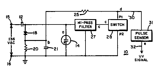
s l~ng fi~st to Figs. 1 and 3, ~c simplL~ed embodiment of ~e
invendon d~d ~erein disclose~ ~eessal~al;fea~es of ~ on. In Pig. l; ~ :
a ~JV de~dor ~be 14 of ~e discha~ge fype is locatod to alIow the uItraviole~
Iadiatio~ to be de~ec~d to impinge on it and in re~on~c ~e U~ hlbe 14 by
discb~ing changes impcdancc when a ~la~vely large voltagc is placed a~oss its
lo ~minals. A disch~ge detcc~on circuit 10 ls used to ~e~ate the UV ~be 14, and has
power ~als 15 and 16 ~i~g 136 VAC 60 hz power from a t~ansfonner
so~c f~ driving this ci~cuit. A reladvd~ làrge capacitor 12 whos~ lralue ~s
prd~ly 2.2 ~fd has one terminal connected bD pDwer te~minal 15. Ihe second
~mi~l of ca~citor 12 is connec~d to a first tenninaI of a ~be dnverdiode l8, this
~s first ~ compnsing in ~is embodîment the anode. The second tenninal of diode
- 18, ~hown as its cathode, is connected to a firstt~l of a tu~e driver re~stor 20.
The ~ t~minal of resistor 20 is connecfed to the second power terminal 16 and a
sooo~d be~nal of a UV tube 14. An ou~ut ddvcr capacitor 21 is connected in
par~d w~h ~or 20. UV tube 14 bas its first term~ conne~t~d ~ the second -~
~al of q~ilor 12. Power termin~ 16 and the second ~minal of W ~be 14
a~ bo~ ~n as ~ in Fig. 1. It is tbuefille conv~ent to rcfcrcnce other
1_ to fflîs ~wnd potential of 0 v., ami the wavefonns of Pig. 3 a~e so
~d. The peak voltage of each wavel~rm is shown on its own ordinate. The
wa~ms of Fig. 3 share ~e sa~ timebasc. Thc re~de~ sho~d note that thc actual
vdlapam~des shown in the waveforms of Fig. 3 a~e approximate and only
~le;f~e~g ~n of ~e ciwits of Figs. 1J 2, and 4,
rol~age on the fi~st t~ a~ tu~e 14 is sho~m as waveform
.
am~:ig. 3, and i~ point of aoc~ on Flg. 1 atpoint a~ The voltagc atpointais
of cou~ illage acr~s llV tube 14. S~long as thercis no ~ avioIet~ia~on
imE iogiDg on ~IV ~be 14, its impodanoe ~mains ve~y high ant voltagc across tube14 is~not affected thereby. 'rhis contibon is show~ in ~e firs~ ~e complete aycles
of w~m a aRa steady state has boen ~hed. It is assumed that ultraviolet
: Ddiati~n be~ns to f~ll on UV tube I4 betwoen c3rcles 3 and 4.
Beore ult~aviolct radiadon ~egins to impinge on UV tube 14, ~e AC
pow~ between lenminals 15 and l6 is half wave rectified by diode 18, thereby
cau~ng ca~acit~r 12 to charge to one-half ~e peak to pe~ voltage o~ the power
wavc. Wl~ ~e 136 VAC designation indicating tbe RMS ~alue, this means that
when s1eady state is reached as sbown between c~cles 0 and 3, capacitor 12 is charged
WO 93/11390 2 1 1 6 8 6 ~ PCI~/US92/10594
^S-
to about 192 v., plus to minus from its first to second terminal. Once capacitor 12 is
fblly charged, the voltage at point a vanes from 0 to -385 v. as shown in Fig. 3,
waveform a.
UV tube 14 in this embodiment conducts when the voltage across its
5 lerminals e~ceedsapproximately 230 v., and once it starts conducting, has an internal
voltago drop of around 180 v. W tube 14 discharge is shown after cycle 3 in Fig. 3.
wa~eform a, voltage at point a faUs from -230 v. to about -180 v. during each
negative-going portion of the AC power wave. The charge on capacitor 12 of + 192v. is added ~ the voltage of the negative-going power wave to shift the voltage at
poht a to -230 v., causing W tube 14 to fire. The voltage across it immediately
drops to -180 v. or less as it begins to conduct. In the preferred embodiment of Fig.
4, an impo~nce in s~ncs with ca~citor 12 and W tube 14 is present to prevent
e~coes~ve cu~t flow through W tube 14.
~onduction by W tube 14 continues un~l the voltage at point a falls
15 below some ~sbold value, at which time the voltage at point a assumes a sine wave
shape again. The voltage at point a then rises above 0 v. in order to replace charge
on ca~citor 12 which was removed by current flow through UV tube 14. Part of this
~ecba~ing cu~ent flows through resistor 20 and part of it flows through capacitor 21,
tbe~eby creating a charge and consequent voltage on capacitor 21 shown by waveform
20 b. Ova a pe~iod of seve~al power cycla, a charge in the ndghborhood of +S0 v.fo~m~ at point b ansing from the current flow ~rough UV tube 14. However, the
first ~ W ~be 14 disc})arges into conduction, there is no voltage on capacitor 21,
and thercforc ~e first discharge, during cyclc 4, does not produce a corresponding
~e~vo-goi~g voltage spike at point d. Subsequent negative-going spikes at point d
25 booome ~y longer as the voltagc on capacitor 21 increases.
The voltage at the first terminal of UV tubc 14 is applied to the input
l~nal of a bigb pass filter 27 whose common terminal is connected to the second
b~min~ of thc UV tubc 14. The output signal of high pass filter 27 is applied to the
control (~ taminal of switch dement 28. High pass filter 27 provides at its output
30 l~minal an oulput signal comprising only the steep wave front pordons of the filter
input sign~, shown as the positive-going spikes in waveform c. Each time UV tube14 ~egins to conduct, the voltage at point a rises very quickly and only this voltage
change can pass through filter 27.
Switch element 28 will typically include several components such as
3s thosc shown in Pig. 4, but for purposes of explaining this simplified embodiment, is
sllown as a block element. Switch element 28 is defined as conducting from the Pl to
the P2 power ~minals when voltage at the C terminal rises above the ground voltage
more than a few volts, and not conducting otherwise. The Pl power terminal of
WO93~1I390 - 211 5 8 6 ~ Pcr/us92/loss4
~ ,.. .
s~tch 28 is connected by an output driver resistor 25 to the first te~inal of ou~put
ddve~ ca~tQr 21. As explained above and- shown in waveform bt once W tube 14
b~ to conduct, ~e voltage at point b begins to rise as part of the recharge current
for ~tor 12 also flows into capacitor 21. Thus the voltage at po~ult d, power
5 tuminal P1, also begins to rise as shown in waveform d. Each time UV tube 14
begims to conduct, tbe steep wave fro~ts pas~od by ~igh pass filter 27 momentarily
d~ive switch 28 into conduction, causing the voltage at point d to fall t~ near 0 v. as s
showll by ~he very na~ow negative-goL~g spik~ s of waveform d. After a few cycles
of conduction by ~JV tube 14, a steady st~e voltage of around +50 ~. at point b is
10 ~eachcd~ and cach momenta~y conduction by switsh ~8 causes this voltage as shown at
point d ~ fall to ground potential dunng switch 28 conduction. It can thus be seen
tbat pulses as ~hown in wavefonn d can occur only if UV tu~e 14 is conducdng on
negative balf ~ es of the AC power, and there are steep wave front features in ~e
voltag~across UV tube 14. If there is no signi~icant conduction by ~JV tube 14,
15 c;~itor 21 will not be charged and the ~oItage at point b will stay nea~ 0 v. If tkere
are no stee~ wave f~ont features in ~e voltage across UV tube 14, ~en no negative-
g~dng pulses ~11 appear at point d. Thus high resistance shunts across pV tube 14
will not beTea~n~ed as indicating presence of ultraviolet radiation.
A p~se sensor circuit 31 is connected by a path 3a to the Pl power
20 ~ of switch 28. P~se sensor ~t 31 counts the numbe~ of pulses m a fi~ced
m~ oro~OEwise detecs or p ocases tflesepulses, to th~y indicabe ~at
~avi~aet Ddiation is impinging on ~V tube 1~.
A particular ~pe of pulse sensor carcuit 31 is shoqn in Fig. ~. An
ilavcrter 33 ~es the signal ~e~resented by waveform d and produces ~ ve-gohg
25 ~ at poi~t g cd~ to the negat~ve-going spibes of waveform d. Since all
of 1hc demen~ shown in Fig. 2 are logic levd devices~ it is noces~ to hold the
i~rollag~ on pa~h 30 from ~e analog components of pulse de~oction circuut 10 to a
vdy Io~ l~:veil, so a 5 volt zener diode ~2 pe~rms ~is fimc~Qn, holding voltage
at pa~ ~ to a maximum of +5 v. Resistor 36 ~mits flow of cu~ent f~om the pulse
30 de~ectian c~t 10 to ~e inverter 33.
A counter 34 recenres the wave~orm g signa~ on sr~ increma~t ~INCR)
input teeminal f~om invater 33. Counter ~4 maintains an intemàl numcnc count
~ralue which is inc~ted each time a positive spikei occurs in waveform g. Each
~ne a pos~tive~going edge occurs on a clear ~ înput terminal this internal count35 value is set ~ zero.
A 100 ms. clock element 36 produces a pulse at point f every 100 ms.
as shown in waveform f. While this clock 36 is shown as issuing its pulses in phase
unth ~e power wave of waveform a and may even be derived` from ~e power wave,
WO 93/11390 2 1 1 6 8 6 6 Pcr/usg2/lo594
-7-
this phase relationship is not necessary. The reader will understand that a 100 ms.
clock pulse oocurs each sLsth power cycle for the standard 60 hz. power wavcformused here. Ea~:h cloclc pulse is applied to the clear (CLR) tenninal of counter 34
tluough an amplifie¢ 35 creating a short delay in the signal as applied to the CLR
s ~minal. The internal value recorded in counter 34 is set to zero by each pulse issued
by clock 36.
The intemal value in counter 34 is rnade available for a test element 38
which senses whe~er the oount value in counter 34 is two or greater, or less than
two. If greater than or oqual to two, a voltage signal encoding a logical 1 value is
o placod on the YES output termi~l of element 38, and the NO output dement carries
a voltagc signal encoding a logical 0. If ~e contents of test element 38 is 0 or 1, then
these lo~ alues on the YES and NO output terminals are revased, with the YES
terrninal ca~ying a logical 0 and ~e NO terminal calTying a logical 1. ;;
Ihe YES and NO output signals from test element 38 are applied to
input.~minals of ~ND gates 39 and 41 respecdvely. Second input tenninals of
AND gates 39 ~nd 41 cach ~oceivc the clock signals from clock element 36. The
output tenninals of AND gates 39 and 41 are connected respectively to the set (S) and
reset ~ minals of a D flip-flop 43, whose ~ I n output terminal provides the UV
signal on pa~h 32 and as shown in Fig. 1.
Wha~ver two or more posidve-going spikes are presel t in the output
of imrert~r 33 within onc 100 ms. interval, test dement 38 sens ~at the contents of
a~:r 34 arc oq!lal to or ~ater than 2, and a logical 1 is applied to thc S input~ of fli~flop 39 wh*~ thc clock pulse defining the end of the 100 ms. interval
o~Nrs. Thc dolay of amplificr 35 prevents clearing of counter 34 until the signals
ca~d on tbe ouqlut tminals of test dement 38 have been gated by AND gates 39
a~d 41 t~ fbp 43. So long as there a~e at least two discha~ges of UV tube 14
~hin e~ch 100 ms. inten~al, it can be safely assumed that a flame is present and_g ~vicla ladiatioli. It is obvious that different applicadons might require
mo¢c discha~ of UV tubc 14 within a l00 ms. inten~al, and this can be easily made
~ simply cbanging the tlueshold of test element 38. Assunung that there had beenno discha~ges of UV tube 14 for a period of time prior to thdr start in cycle 3, the
ut of flip~bp 43 dwvn u waveform e will encode a logical 0 value. When two
podtiv~ spibes occur vnthin the l00 ms. interval defined by power cycles 1
~rough 6, ~en the logical value encoded by the "1" output of fli~flop 43 changes3s from a logical 0 to a logical 1 within cycle 6 as shown in waveform e.
The CiICNit of Fig. 4 is an operational embodiment of ~his invention. It
is quite similar in several respects to the circuit of Fig. 1, and for t~.is r~son the
similar components and elements have been given similar reference numbers. Since
W~93/ll3gO 2116 8 6 fi P~tUS92/10594
the a~a~on of much of ~ese two circuits is similar, it is convenient to desc~ibe the
pu~pose and function of ody those elements of liig. 4 not shown in Fig. 1. Capacitor
55, connectod between ~e powe~ ~inals 15 and ~6 removes high and m~d-~ange
*e~c3r noise f~om thc power wave. ~Foltage regulator 36 fur~er limits dle
5 poten~al dis~ion in the power wave by limiting the m~num voltage dif~erence
between pow~ ~minals 15 and 16 to less than 270 ~.1 Resistor 53 is in ~es wi~
ca~citor 12, and limits current flow ~ough ca~citor 12 and W ~ube 14 to prevent
complete disch~ge of capacitor 12 when tube 14 fires. Resis~or S0 ls connectod in
par~ld w~th ca~citor 12 and provides a high re~stance ~unt for bleeding dangerous
10 voI~ge le~els from ca~citor 12 when the circuît is not ~n use. Diode 38 ~lso shunts
capacitor 12, and its polarity is such that capa~itor 12 cannot charge n4~ative to
po~tive f~om left to right. If capacitor 12 is chosen as Wng of a pol~uized ~pe, it is
thus protected ~m damage a~ng from c~g in ~e wrong di~ection.
Capacitor 60 and resistor 61 form high pass filter 27 as shown,
15 G~pacitor 6~ baving a value of around 500 pfd. so as tl> substan~ally an~nua~ all
very s~p voltage changes ac~oss ~JV tube 14. W~thin switch d~nent 28,
zener diode 57 dmps the voltage p~ovided by the output of high pass filte~ 28 by a
fi~ed amount. Resistors 62 and 65 divide the voltage dro~ed by zener diode 57 toprovide ale~d for driving into conduction at thepr~per dme the Uan~slor 68 whichzo ye~ms tbe a~ switching fimction with~ switch element 28. l~iode 64 prcvents
damagc a~g f~om thc voltagc on the base of t~ansistor 68 from f~lling more than
onc diodedrop bdow the emitter. Tlle emitter and collector of ~stor 68
~especd~dy fo~n power terminals P1 and P2 as shown.
T~e circuit of Fig. 4 embodies apulse sensor 31 which does not
25 p~ea direct logic sig~al indicadng ~ presence or absence of ultraviol~ ~adiadon
impingimg on IJV t~bc 14. Instead, thepulse sensor ~1 of Fig. 4 c~mpnsesan analog
oonveder w~ich mimics the output of a fl~une rod de~ector. The voltage on ~a~acitor
21 is a~pL;et to a caE~citor 70 th~ough resistor 25, caus~ng ca~tor -70 to charge
tbrough ~r 71 to a vollage level near that of cap~citor 21. Thc reader ~dll see
3~ capacitor 70 is ~e~eby charged posi~ve to negati ~e from left to right. l!he value
of ~itor 70 is selectod to be approximalely an order o~ magni~udc sm~ler tha~ is~cilor 21 so tbat the amount of charge hdd ~y capacitor 70 is much smaller ~an
~at beld by ca*citor 21. Each negative-going ~pike atpoint d of Pig. 4 pulls the left
temdnal OI' ca~citor 70 to ground, and for the duration of the ~pike driving the35 voltage atthe connecdon point h to a negative leveI whose absolute value equals the
value of the posidve voltage carried on capacitor 21 at point b.
A san~le and hold circuit comprises a sampling diode 73, sampling
capacitor 75, and sampling resistor 79. Diode 70 hàs its cathode connected to point
Wo 93/11390 2 1 1 6 ~ 6 6 Pcr/uss2/l0594
.
h, the right termir~ of capacitor 70. The anode of diode 73 is connected to a first
teanin~ of sampling capacitor 75 with the second terminal of capacitor 75 connected
to g~ound. Sampling resistor is connected between ground and the anode of diode 73.
Each timc point d is pulled to ground, the voltage at point h is pulled down to a
5 nega~ve voltagc equal to thc voltage across capacitor 70, as is shown by the negative-
going ~ces in wavcform h of Fig. 3. The value of capacitor ?5 is roughly an order
of magni~de smaller than ~e valuc of ca~acitor 70. Each time a negative-going
~pibe in wavefQrm h occurs, a portion of thc charge on capacitor 70 is ~ansfcrred to
capacitor 75 as is shown by the negative-going transitions in waveform e' in Fig. 3.
~a Oncc the voltagc at point h ~eturns to near ground, diode 73 cuts off prevendng the
vol~ge at point h from affocdng the acdvity of diode 75 and resistor 79. The charge
placed on capacitor 75 each timc point h is pulled negative then creates a current flow
through resistor 79 when a high impedance usage device is attached tO terminal 32. A
~V signal current flows into terminal 32 through the usage device and produces a15 negative W signal voltage at terminal 32 shown as waveform e'. The charge on
capa~itor 73 slowly dissipa~es th~ough resistor 79 and the usage device as is shown by
~e slowly rising voltage in waveform e' between the successive instants capacitor 75
rec~ves charge from capacitor 70. By proper choice of the various components in the
circuit of Fig. 4, the cu~rent flow into terminal 32 will be very similar to that
2~ cba~is~c of a flame rod sensor.
wo 93JIl3go 2 1 1 6 8 ~ 6 PCr/US92/I0594
-10- .
In my prefe~red embodiment, ~e vanous components of Pig. 4 have
~he values shown in ~e following table:
Resistor 53 9IOS1
Capacitor SS .002~ ~fd,
5- Capaator 12 2.2~fd.
Diode 38 t~pe ~N4004 7
Resistor S0 100 megS2
I)iode 18 ~pe 1N3195
Capacitor 62 4.7 ~fd.
~0 Resistors 63, 67, and71 lO,OOOn
~esistor 20 8,200SI
~tor 21 4~7 ~fd.
Resistors 45 and 71 l,ooon
Capacitor 6û S00 pfd
~5 Resistor 61 5I,000~2
Zener diode 57 10 v.
Diodcs 64 and 73 t~pe lN4148 ::
ResIstor 65 200,000~2
Transist~r 68 t~e MP~8
20. Capasitor 70 .47 ~fd.
Capacitor 75 .033 ~d~
Resistor 79 2~94 megn