Note: Descriptions are shown in the official language in which they were submitted.
21 1723~
CAPACITOR MOUNTING STRUCTURE FOR PRINTED
CIRCUIT BOARDS
The field of this invention relates to the
mounting structure for a capacitor onto a printed
circuit board in order to minimize parasitic
inductance.
It is well known in the art of printed circuit
board design to utilize capacitors to smooth the
effects of sporadic current peaks and noise which is
typical of electronic circuity. Theoretically, a
capacitor has the characteristic of maintaining a
substantially constant voltage while absorbing applied
current changes, which is a typically important
function in computer circuit design where current
surges and peaks due to noise and the like must be
smoothed to prevent interference with signal
generation. In other words, capacitors are used to
stabilize the supply voltage by compensating for abrupt
current changes.
However, due to the application of current across
a capacitor, the capacitor generates an inductance
called "parasitic" inductance. And, just as in the
case of an inductor, such parasitic inductance can
limit the rate of current change across the capacitor
and thus cause the voltage to drop in spite of the
presence of the capacitor. Further, such parasitic
inductance can change the RF impedance characteristics
of capacitors making them more complex elements in RF
2 ~ .~
(radio frequency) applications, which makes design more
complicated and performance objectives more difficult
to achieve.
Methods have been tried to reduce parasitic
capacitor inductance. One method is to reduce the
length of conductor traces extending between the
capacitor terminal and the pad of a via. Another
suggestion is the widening of capacitors and traces and
shortening or eliminating traces from the capacitor
pads to vias. However, there is a lower limit on
capacitor lengths. For example, if a capacitor is too
short, there is not enough space between the metalized
contacts located at the ends of the capacitors and
solder bridging to the metalized contacts or terminals
becomes a problem. Capacitor shortening can also be
difficult where board fabrication processes set the
minimum space between vias, which dictates the minimum
total length for the capacitor and the mounting
structure combined. Increasing capacitor width at
minimum length increases space occupied by the
capacitor which uses more board space. In addition,
there is a limit to the ratio of width to lenath in
capacitor fabrication. Even with maximized capacitor
width, within the practical range of capacitor and
trace widths, inductance can only be reduced 30-40%.
This invention is directed to a capacitor mounting
structure for printed circuit boards which
substantially minimizes parasitic capacitor inductance.
In the capacitor mounting structure of this invention,
the vias are mounted under the central section of the
capacitor and in general alignment with each other.
The pads which electrically attach to the vias include
~ ~ ~7~3~
-3-
extensions or digits which provide for interdigitated mounting
of the conductor pads to the vias.
Such a capacitor mounting structure includes the following
specific components. The capacitor includes a central
dielectric section and first and second opposing terminals. A
printed circuit board includes an upper surface for receiving
electronic components such as the capacitors and has first and
second conductor planes generally parallel to the upper surface,
one or both of the conductor planes being imbedded in the
printed circuit board.
In one embodiment, first, second and third vias are mounted
in the printed circuit board underneath the central dielectric
section of the capacitor. The three vias are in alignment. The
two outside vias are electrically connected to a first via pad
while the via located between the first two vias is electrically
connected to the second via pad, the via pads or footprints
being soldered to the opposing terminals of the capacitor. With
positioning of the interdigitated traces and vias directly under
the dielectric section of the capacitor, the magnetic field
which forms between the capacitor and the traces is confined in
a strait formed by the capacitor and the traces. The higher the
ratio of the length of the strait to the narrow dimension of the
strait, the lower the resulting inductance. The proposed
structure minimizes inductance by minimizing the distance
between the capacitor and the traces. An alternative
construction provides first and second vias wherein the first
via includes a substantially flat conductive pad which is U-
shaped to provide opposing, spaced apart mounting digits and the
second vias flat conductive pad includes a digit interposed
between the spaced apart mounting digits of the first conductive
pad.
In another embodiment, the invention provides a capacitor
mounting structure for printed circuit boards wherein the
capacitor includes first and second terminals which are
connected to first and second conductor planes in the printed
circuit board in a manner to minimize parasitic inductance. The
structure comprises a capacitor including a central dielectric
2 1 1 7 2 3 ~
-3A-
section and first and second opposing terminals, the first and
second opposing terminals being spaced equidistant from a
transverse vertical centerline through the central dielectric
section. A printed circuit board has an upper surface for
receiving electronic components including capacitors, the
printed circuit board including first and second conductor
planes generally parallel to the upper surface, at least one of
the conductor planes being imbedded in the printed circuit
board. First and second vias are mounted in the printed circuit
board, each of the vias including a tubular conductor section
and a substantially flat conductive pad extending from one end
of the tubular conductor section, the first via being
electrically connected to the first conductor plane and the
second via being electrically connected to the second conductor
plane. The tubular conductor sections of the first and second
vias are positioned immediately adjacent to each other between
the first and second terminals of the capacitor and beneath the
capacitor central dielectric section and aligned along a
vertical plane of the transverse vertical centerline with the
capacitor being mounted onto the upper surface of the printed
circuit board with the first and second terminals of the
capacitor being electrically connected to the first and second
conductive pads of the vias thereby minimizing parasitic
inductance associated with the capacitor.
The summary of this invention is not intended to be
exhaustive of the patentable features of this invention, which
are set forth in the claims to be read in view of the
specification.
- ~117239
Figs. 1 and lA illustrate a prior art structure
mounting a capacitor onto a printed circuit board
wherein the vias are positioned away from the capacitor
terminals;
Figs. 2 and 2A-B illustrate a capacitor mounting
structure wherein the vias are located underneath the
capacitor but in a position of non-alignment;
Figs. 3 and 3A-B illustrate the capacitor mounting
structure of this invention; and
Fig. 4 illustrates the minimization of inductance
generated by this invention.
The problem of parasitic inductance in printed
circuit board design is well known. Figs. 1 and lA-B
illustrate a known mounting structure for a capacitor,
which mounting structure creates undesirable levels of
parasitic capacitive inductance. In Fig. 1, the
printed circuit board B is represented by a first or
upper conductor plane 10 and a second or lower
conductor plane 11 which, in a well known manner,
commonly provide power to the entire board. PCB board
B includes upper non-conducting surface lOa. A first
via 12 is electrically connected to the second
conductor plane 11, which may be a voltage or power
plane. The tubular conductor section of via 12 is
shown as extending through an opening lOb in the upper
conductor plane 10, which may be a ground plane, such
that the via is not electrically connected to the
ground plane. The tubular conductor section of via 14
is electrically connected to the upper or ground plane
at lOc but extends through opening lla in the voltage
plane 11. The utilization of vias 12 and 14 to provide
~11723~
electrical connection to various conductor or ground
planes in a printed circuit board is well known.
The capacitor 15 is illustrated as being mounted
in between the vias 12 and 14. The capacitor 15
includes metallic terminals or caps 15a and 15b located
at each end of the capacitor. The capacitor middle
section 15C represents the central dielectric portion
as is well known in the art. It is also known to
connect capacitors such as lS to the printed circuit
board B through conductor pads or footprints 17 and 18
which are mounted onto the upper surface lOa of the
printed circuit board. The capacitor 15 is
electrically attached to the conductor pads 17 and 18
utilizing soldering techniques which produce the solder
fillets 18 and 19 illustrated in Fig. 1. Electrical
connection from the conductor pad 17a to the via 12 is
provided by conductor line or trace 20. In the similar
manner, a trace 21 extends electrical connection from
the pad 18 to the via 14. In this manner, the
capacitor 15 is mounted onto the printed circuit board
B.
However, the mounting structure illustrated in
Figs. 1 and lA cause undesirable parasitic inductance
during operation. Referring to Fig. 1, the area which
can be considered as generating the parasitic
inductance is located between the vias 12 and 14, above
the ground plane 10 and below the traces 20 and 21,
conductor pads 17 and 18 and the bottom of the
dielectric portion 15C of the capacitor. This area,
defined by the letter I, is the critical region which
causes the generation of parasitic inductance. While
the area I is described as influential on generation of
parasitic inductance, technically, it is the aspect
ratio that must be minimized, which is the width w of
capacitor 15 divided by the gap thickness or distance d
211723~
between the bottom surface of the capacitor and the
ground plane 10. The aspect ratio w/d is critical
since it describes the effect of the strait on the
magnetic field. As this aspect ratio w/d increases,
the reluctance increases, which decreases the parasitic
inductance generated. Stated another way, if the
effect of the distance between capacitor solder pads is
included, maximizing the aspect ratio of capacitor
width to area I will minimize parasitic inductance of
the capacitor.
Such undesirable parasitic inductance limits the
rate of current change in pulse applications. For
example, capacitors 15 are often used to stabilize
supply voltages when the current increases abruptly.
The presence of parasitic inductance limits the rate of
current change and causes voltage to drop in spite of
the utilization of capacitors. Further, inductance
changes the RF impedance characteristics of capacitors,
making them complex elements in RF applications, which
makes design more complicated and performance
objectives more difficult to achieve.
It is known to reduce capacitor inductance by
reducing the length of traces such as 20 and 21 and or
widening the capacitor 15, and even eliminating traces
from capacitor pads to vias by placing the via within
the pad.
For example, Figs. 2, 2A and 2B represent one such
solution. The same numbers and letters will be used to
describe the same elements. In Fig. 2, the capacitor
15 is actually mounted over vias 30 and 31. Via 30 is
illustrated in connection to power plane 11 and via 31
is electrically connected to ground plane 10.
Referring to Figs. 2A and 2B, a rectangular conductor
pad 30a is mounted over via 30 and similarly, a
rectangular connector pad 3la is mounted over via 31.
211~3
The metalized ends or caps 15a and 15b are electrically
connected to the conductor pads 3Oa and 3Ob,
respectively, by solder represented by soldering points
32 and 33. Referring now to Fig. 2, it can be seen
that the area I' defined by the ground plane 10, vias
30 and 31, and the bottom surface of the central
capacitor section 15c is a much smaller area than area
I shown in Fig. 1. The reduction in the area I to I'
thus reduces the amount of parasitic inductance
generated during operation of the circuitry.
Another suggestion to reduce parasitic capacitance
is to increase capacitor width and minimize capacitor
length. However, an increase in the width of the
capacitor increases the space necessary on the surface
of the PCB board to accommodate the capacitor.
Further, there is a limit to the ratio of width to
length in capacitor fabrication. Finally with respect
to capacitor width, within the practical range of
capacitor and trace width, inductance can probably only
be reduced about 30-40%.
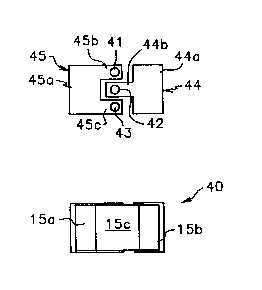
Referring now to Figs. 3 and 3A-B, the capacitor
mounting structure generally designated as 40 for
minimizing parasitic inductance is illustrated. As
before, the same numbers will be used to identify the
same elements. Thus the PCB board generally designated
as B includes the ground plane 10 and power plane 11
and has upper surface lOa. Three vias 41, 42 and 43,
are positioned in substantially straight line alignment
as illustrated in Fig. 3B and are located substantially
adjacent to each other in a row, which row is
approximately aligned with the centerline 50 of the
capacitor 15. The vias 41-43 alternately electrically
connect to either ground plane 10 or voltage plane 11.
As illustrated in Fig. 3, tubular section of via 43 is
electrically connected to the voltage plane 11 and
21172~
extends through an opening in the ground plane 10. The
tubular section of via 42 is electrically connected to
the ground plane 10 and extends through an opening in
the power plane 11. Though not shown, via 41 is
electrically connected to the power plane 11.
The conductor pad or footprint 4i for via 42 is
generally T-shaped and includes a central rectangular
portion 44a formed with an extension or finger portion
44b, which extends into attachment to the top of the
via 42.
The conductor pad 45 for vias 41 and 43, is
generally U-shaped. A central rectangular portion 45a
includes first and second extensions or fingers 45b and
45c which extend into connection with vias 41 and 43.
A U-shaped recess is formed between the conductor pad
extensions 45b and 45c. The conductor pad U-shaped
recess formed between conductor pad extensions 45b and
45c receives the extension 44b for conductor pad 44.
In this manner, the ccnductor pad extensions are
interdigitated with respect to each other, so that
effective electrical connection can be made with the
vias 41-43 in substantially a straight line.
The capacitor end metal caps 15a and 15b are
soldered onto the rectangular portions 45a and 44a of
the pads, respectively. The solder pads 47 and 48 are
applied as thinly as possible, such that there is
little separation or thickness d" between the capacitor
bottom surface and the conductor pads. In this manner,
the cross-sectional area I" between the conductor pads,
the solder points 47 and 48 and the bottom of the
central capacitor section 15C is minimized in area,
thereby minimizinq the distance d" between the bottom
of the capacitor and the pads 44 and 45 wherein
parasitic inductor can be generated. Reduction of the
distance d" between the conductor pads 44 and 45 and
21172~
the bottom of the capacitor 15 maximizes the aspect
ratio and minimizes the generation of inductance by
maximizing reluctance. It is noted that placement of
the conductor pads under the central section of the
capacitor 15 also acts to reduce thickness d".
Referring now to Fig. 4, the effect of the
constriction on parasitic inductance generating region
is illustrated. Constricting the field lines increases
the reluctance of the magnetic path which in turn
reduces magnetic flux and thus reduces inductance.
Further, the interdigitated vias formed by pad
extensions 45b and c and 44b form a low inductance
structure. It is believed that the insertion of the
via 42 between vias 41 and 43 reduces inductance by a
factor approaching 50%. A designer might typically add
a pair of opposing vias (connected to ground and
voltage planes) to reduce inductance roughly 50~;
however, the proposed structure of Fig. 3 achieves the
same benefit with only 3 vias instead of 4.
It is further contemplated that, while the
capacitor mounting structure 40 of Fig. 3 shows 3 vias
in alignment, any number of vias could be added in a
line, such that current would be returned under the
capacitor in a position complementary to the current
flowing through the capacitor, which minimizes
parasitic inductance. It is contemplated that more
vias may be utilized as smaller geometries become
feasible. These concepts can be applied to circuit
boards of various manufacture, whether printed or not.
The advantages of this invention are many.
Reducing the number of capacitors for a particular PCB
will save money in the number of capacitors used as
well as the number of solder points needed. Reduction
in the number of capacitors can also increase lay-out
flexibility and even reduce the over-all size of the
-
2 l 172~
--10--
PCB board needed. As an example of the significance of
this invention, in one example, PCB circuitry using
this invention was as effective with 25 capacitors as a
conventional design of Fig. 1 was with 106 capacitors.
The foregoing disclosure and description of the
invention are illustrative and explanatory thereof, and
various changes in the size, shape, materials,
components, circuit elements, wiring connections and
contacts, as well as in the details of the illustrated
circuitry and construction and method of operation may
be made without departing from the spirit of the
invention.