Note: Descriptions are shown in the official language in which they were submitted.
CA 02117476 1999-02-24
CAMERA FOR PRODUCING VIDEO OUTPUT SIGNAL, INFRARED FOCAL PLANE
ARRAY PACKAGE FOR SUCH CAMERA, AND METHOD AND APPARATUS FOR
GENERATING VIDEO SIGNALS FROM PASSIVE FOCAL PLANE ARRAY OF
ELEMENTS ON A SEMICONDUCTOR SUBSTRATE
FIELD OF THE INVENTION
This invention relates to the art of video imaging
and has particular applicability to video cameras capable of
producing visual images from infrared radiation and even more
particularly to providing such images at relatively low cost.
BACKGROUND OF THE INVENTION
This invention applies to a new type of radiation-
sensitive focal plane operating near room temperature: a two-
dimensional array of microminiature bolometers
(microbolometers). This invention describes 1) an apparatus
and method of using such focal planes in an IR imaging camera
without the necessity to 'use a chopper; 2) an apparatus and
method for efficiently retrieving the information contained in
the focal plane; and 3) a camera system in which these focal
planes can operate to produce video output signals.
SUMMARY OF THE INVENTION
The camera system described in this invention has a
radiation receiving system including preferably a lens,
reflective or other optical system assembly with an iris to
focus the scene on a focal plane array contained within a
vacuum chamber. The light receiving surface or "window" of
the vacuum chamber is invisible to the wavelengths of
~
CA 02117476 1999-02-24
- 2 -
radiation desired to be recorded or received by the focal
plane array.
The vacuum package contains the focal plane array
affixed to one surface of a thermoelectric temperature
stabilizer. On the thermoelectric temperature stabilizer or
the substrate of the focal plane array is a temperature
sensing device. This whole assembly is then fixed into the
base and supporting structure of the vacuum chamber.
Electrical connections are made through the wall of the vacuum
chamber to the various components within it and this allows
for a bias current to be pulsed to specific focal plane array
elements at specific instants in time so that they will
produce an output related to the radiation received thereby.
Control leads for the thermoelectric temperature stabilizer
also pass through the vacuum chamber and allow for it to be
temperature stabilized based on the temperature sensed by the
temperature sensor. A high stability bias source provides
voltage at a constant level to be sent via a decoder to the
particular focal plane array elements to be sensed in a sweep.
The output of each element is received by a preamplifier, the
output of which is translated into a digital signal and
forwarded to an image processor which produces a video output.
In the preferred embodiment, the window to the
vacuum chamber through which the radiation passes is
transparent only to infrared and the focal plane array
consists of microbolometer elements appropriately spaced upon
the array to dissipate heat similarly to the microbolometer
64159-1352
CA 02117476 1999-06-25
- 3 -
focal plane arrays described in U.S. Patent Serial Nos.
5,220,188 and 5,220,189 both of which issued 15 June 1993.
In accordance with the present invention there is
provided an infrax-ed camera having: optical assembly which
brings light/infrared radiation to a focal plane array of
infrared sensitive' microbolometers on a semiconductor
substrate that is maintained constantly at any selectable
temperature, over a wide range, by a thermoelectric
temperature stabilizer wherein said thermoelectric temperature
stabilizer is regulated by a controller which maintains
temperature based on a signal received from a temperature
sensor in close thermal association with said array.
In accordance with the present invention there is
further provided a.n apparatus for maintaining a semiconductor
device at relatively constant temperature in a vacuum
comprising: a substrate having first and second surfaces with
an aperture formed. therethrough, said aperture being
surrounded along with an area of said first surface by a
contiguous wall structure, said area inside said wall being a
bounded surface area, a thermoelectric temperature stabilizer
mounted firmly to said bounded surface so as to allow for
fluid communication through said aperture, and having an
opposite surface, said semiconductor device being mounted to
the opposite surface of said thermoelectric temperature
stabilizer, a temperature sensor mounted to said semiconductor
device in thermal proximity to said sensor array, a window for
admitting some radiation to said semiconductor device mounted
64159-1352
CA 02117476 1999-06-25
- 3a -
to seal in said thermoelectric temperature stabilizer,
temperature sensor_ and semiconductor device in the interior
space definable b;r said first surface, said window for
admitting some radiation in and said wall structure.
In accordance with the present invention there is
further provided an apparatus for maintaining a sensor array
at relatively con:~tant temperature in a vacuum comprising: a
substrate having first and second surfaces with an aperture
formed therethrouc~h, said aperture being surrounded along with
an area of said first surface by a contiguous wall structure,
said area inside .said wall being a bounded surface area, a
thermoelectric temperature stabilizer mounted firmly to said
bounded surface so as to allow for fluid communication through
said aperture, anc~ having an opposite surface, said sensor
array being mounted to the opposite surface of said
thermoelectric temperature stabilizer, a temperature sensor
mounted to said sensor array in thermal proximity to said
sensor array, a window for admitting some radiation to said
sensor array mounted to seal in said thermoelectric
temperature stabilizer, temperature sensor and sensor array in
the interior space: definable by said first surface, said
window for admitting some radiation and said wall structure.
In accordance with the present invention there is
further provided a.n apparatus for maintaining an infrared
sensitive semiconductor device at relatively constant
temperature in a vacuum comprising: a substrate having first
and second surfaces with an aperture formed therethrough, said
64159-1352
CA 02117476 1999-06-25
- 3b -
aperture being surrounded along with an area of said first
surface by a contiguous wall structure, said area inside said
wall being a bounded surface area, a thermoelectric
temperature stabilizer mounted firmly to said bounded surface
_ so as to allow fo:r fluid communication through said aperture,
and having an opposite surface, said infrared sensitive
semiconductor device being mounted to the opposite surface of
said thermoelectric temperature stabilizer, a temperature
sensor mounted to said infrared sensitive semiconductor device
in thermal proximity to said sensor array, a window for
admitting some radiation to said infrared sensitive
semiconductor device mounted to seal in said thermoelectric
temperature stabi:iizer, temperature sensor and infrared
sensitive semiconductor device in the interior space definable
by said first sur:Eace, said window for admitting some
radiation and said wall structure.
In accordance with the present invention there is
further provided a method for reading out changes in
resistivity of passive radiation receiving units in an n by m
array including: exposing the radiation receiving surface to
an irradiated scene desired to be observed, thus developing a
change in resistivity of said receiving units related to the
amount of radiation received from said scene, sweeping the
receiving units w_Lth a short duration pulse of bias current
that heats the sensors and is too large to allow said units to
remain stable if said pulse is of a substantially longer
duration wherein said sweep is at such a rate that each said
64159-1352
CA 02117476 1999-06-25
s,
- 3c -
unit has time to .return to a stabilization temperature before
the sweep generates a second short duration bias pulse to each
said unit.
BRIEF DESCRIPTION OF THE DRAWINGS
Figure :L is a three-dimensional block diagram of the
major components of the preferred embodiment camera.
Figure :? is an exploded view of the vacuum package.
Figure 3 is a side view of the vacuum package.
Figure 4 is an electrical block diagram of a small
heuristic focal plane array in accord with one embodiment of
the invention.
Figure 5 is an electrical wiring diagram of a small
section of the drive circuitry associated with the preferred
embodiment focal plane array.
Figure 6 is a graph of time versus temperature and
voltage illustrating the effect of the application of pulse
bias voltage to the passive elements of the focal plane array
over time.
DETAILED DESCRIPTION OF THE PREFERRED EMBODIMENTS
The Camera
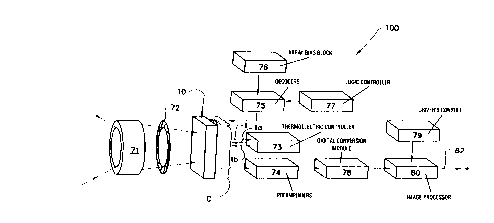
Referring first to Fig. 1, the layout of the camera
100 is shown. Light or radiation received by the lens or
reflective optica7_ system 71 enters through the iris 72 to the
surface of the window on the package 10 or vacuum chamber 10
containing the focal plane array (not shown). Small dotted
lines c indicate that many pins connect the package 10 to the
rest of the camera electrically.
64159-1352
CA 02117476 1999-02-24
- 4 -
The temperature of the focal plane array is kept
constant by a thermoelectric controller 73 which sets the
temperature based on the output of a temperature sensor inside
the package 10. The temperature at which the array is kept is
referred to as a stabilization temperature. For the
microbolometers we used, the range at which this has been
tested is from zero to 30°C, although there is no reason much
higher or lower stabilization temperatures could not be used.
A line t indicates that temperature information is
received by the thermoelectric controller. If the temperature
information is what is desired, no signals will be sent over
the other lines to and tb. However, in the preferred
embodiment the thermoelectric controller will be controlled by
sending power over either line to or tb depending on the
direction (warmer or cooler) of the desired change in
temperature.
The passive elements of the focal plane array in the
package 10 need to be polled or interrogated by providing a
voltage or a current. Accordingly, an array bias is produced
by an array bias block 76, this electrical unit being a highly
stable (low noise, low drift) voltage supply in the preferred
embodiment. The inventors have had some success using a
simple battery, although certainly other sources well known to
those in the art could be employed. The voltage must be
provided to the passive elements in the array in some sequence
in the preferred embodiment. Accordingly, a set of decoders
75 is used which is controlled by a logic controller 77. The
64159-1352
' CA 02117476 1999-02-24
- 5 -
logic controller 77 will steer the current by controlling the
decoders (essentially operating as a large multiplexer) in a
weeping sequence such that each row by column address is
polled over a sweep one time before being polled again in the
second sweep. The decoders then steer the bias current
provided by the array bias 76 to the appropriate pins c
attached to the package 10.
Output pins c are all connected to a set of
preamplifiers illustrated here as block 74. The output of
these preamplifiers may be taken either serially or in a
buffered form by an analog to digital conversion module 78
which can then provide a digital indication of the value of
the analog signal level input thereto for each output from
each preamplifier. The electrical characteristics of the
preamplifier are designed to be stable with time and
temperature or correction for such changes are applied in the
image processor. The inventors have had some success with the
latter technique, employing calibration signals injected into
the preamplifiers. Alternatively, this may be attained by
temperature- and time- independent circuit designs well known
to those in the art.
In this camera, is also provided an image processor
80 to which a driver's console 79 is in electrical and
controlling contact. In other words, by controlling how the
digital values are received which are already in the image
processor, an operator can change the sensitivity, receive
freeze-frame information and variously correct or change the
64159-1352
CA 02117476 1999-02-24
- 6 -
video signal which will be output by the image processor 80.
Image processors are fairly well known in the art of video
cameras and generally use digital signal processing circuits
and various adjustments to the incoming input signal to
produce an output video signal here illustrated on line 82.
Software control is the preferred embodiment since
the algorithms normally used are most conveniently implemented
by software, rather than by hard-wired logic. In this way we
can implement things which are difficult to implement in
hardware, because different algorithms are required at
different instants in time, and because signals from different
areas of the array may be treated with different processing
algorithms.
Some advantages are inherent in this camera design
which are not readily apparent.
The iris may be closed momentarily (e. g., after
camera manufacture, or at camera start-up) to allow the image
processor 80 to average several image frames and store this
digital data in a long-lived digital memory (which may be in
the image processor systems). A simple expedient of a lens
cap or shutter may be employed instead, if desired. During
normal camera operation the iris 72 remains permanently open,
or partially closed if it is desired to reduce the radiation
intensity falling on the focal plane. The image processor
subtracts the incoming signals from the digital data in its
long-lived memory on a pixel-by-pixel basis. This provides
offset correction for each pixel in the image to be viewed by
64159-1352
CA 02117476 1999-02-24
a human observer, a requirement and process well known to
those in the art. Provided the focal plane remains maintained
at a stable temperature by the TE stabilizer, the preamplifier
electrical characteristics do not change, and no change is
made to the array electrical polling, no chopper is required
to interrupt the radiation from the scene. The absence of a
chopper produces many desirable benefits: a cheaper and more
reliable camera, a lower electronic speed requirement, and
elimination of the sensitivity loss produced by the periodic
radiation obstruction of a chopper.
The Package for the Array
Referring to Fig. 2, the vacuum package 10 is shown
in an exploded view. The package consists of a base plate 11
containing apertures 12, 13, 14, and 15 (not shown) for
connecting it to the camera, a surrounding wall structure 16,
having an internal step 17, on which are located pads 18.
Wires 19, of which only a few are shown, are connected to
these pads. Basically, this exploded view and its limited
elements is shown for illustrative purposes only and not to be
taken in a limiting way.
The wall 16 surrounds a bounded area 54 within which
there is an aperture 53 in the upper surface of base plate 11.
The aperture extends into a tube 50 whose inner space is
defined by dotted lines 52 and which in the final preferred
embodiment product is crimped off at 51. A Better 55 may also
be used. A thermoelectric temperature stabilizer 20 fits into
the bounded space 54 in the finished package. The
64159-1352
CA 02117476 1999-02-24
_ g _
thermoelectric temperature stabilizer consists generally (in
the preferred embodiment) of an upper plate 20a and a lower
plate 20b of what is usually beryllium oxide sandwiching a
layer of other material such as bismuth and/or antimony, or
other suitable materials known in the art. Power leads "-"
and "+" provide power to either one of the plates thus either
cooling or warming the device. The surfaces such as upper
surface 26 are metallized for bonding preferably by solder to
either the upper surface of substrate 11 on the one side or
the lower surface of the focal plane array to surface 26. A
temperature sensing device 27 in the preferred embodiment, for
simplicity's sake a thermistor, is also attached to the
surface 26 of the thermoelectric temperature stabilizer 20.
Numerous temperature sensors are currently under development
or readily available and, depending on the economics, may also
be employed. If the temperature sensor is small enough it
could even reside on the focal plane array chip itself. This
would be left up to the needs and desires of the designer.
All that is necessary is that a very accurate reading of the
temperature of the focal plane array be given by the
temperature sensing device.
Also, the inventors have had some success using
temperature sensors fabricated on the focal plane array chips.
These sensors are periodically polled by the focal plane
readout electronics in the same way as the microbolometers,
and the temperature data is sent to the image processor in the
same way as the microbolometer signals. The inventors have
64159-1352
CA 02117476 1999-02-24
_ g _
had some success in using the image processor to use these
temperature signals to improve the image quality by correcting
for small temperature drifts in the cameras. These could be
microbolometers which are intentionally made unresponsive to
infrared radiation.
The focal plane array chip 30 has bonding pads or
leads 31 preferably around its edges. The focal plane array
elements which are sensitive to radiation are in area 33 in
the preferred embodiment chip. If a temperature sensor were
employed on the focal plane array, it would most likely be
preferred to be included in area 33.
Topping off the package is a window 40 which is
transparent to the type of radiation expected and desired to
be received by the focal plane array 33. The lower peripheral
edges of this window should be metallized in the preferred
embodiment to permit soldering. For the most desired
embodiment at the current time, the focal plane array elements
are passive microbolometer elements coated with vanadium oxide
which produce a change in resistivity based on the amount of
infrared radiation received by each element in a way related
to that disclosed in U.S. Patent Application Serial No.
07/035,118. In this infrared sensitive preferred embodiment a
germanium window that is anti reflective is employed for
window 40. In the currently preferred embodiment package, the
base 11 and its surrounding wall 16 is a custom integrated
circuit package produced by Kyocera of Japan made of aluminum
64159-1352
CA 02117476 1999-02-24
- 10 -
oxide (A1203) for the wall with a base plate of a copper
alloy. The preferred embodiment tube is copper and the Better
is a metallic alloy well known to those in the art, activated
far from the device after the tube is used for pumping out the
air within the sealed package 10. The Better is then pushed
up close toward the package in the tube 50 and the package is
sealed off by crimping the tube at 51. In the preferred
embodiment solder is used for everything but electrical
connections which are bonded. However, as technology and
practice improves, attaching the electrical leads and the
components together may be done in different ways within the
scope of this invention. Likewise, any materials which would
readily substitute for those described hereabove may also be
substituted without going beyond the scope of this invention.
Referring now to Fig. 3, a side view of the package
10 is shown having the copper tube 50 bonded to the base plate
11 with the Better 55 inside. The electrical wires, w, wt,
wtb, and wta, provide power and readout to and from the three
devices in the vacuum space 53. The leads or pads on step 17
from these wires are connected through wall 16 to wires 19
which may then be bonded to connectors to external elements
such as the preamplifiers in block 74 of Fig. 1, the
thermoelectric controller of block 73 of Fig. 1, and the
decoders supplying the bias voltage through block 75 of Fig.
1. Radiation which reaches the window 40 in the right
wavelength (R1) will go through the window. Radiation which
is not of the right wavelength (R2) will be reflected off of
64159-1352
CA 02117476 1999-02-24
- 11 -
the window 40 or absorbed by it. As stated before, the
various surfaces are held together in the preferred embodiment
by soldering such that joints 61, 62, 63, and 64 would be
solder connections. As also described before, these
connections may be made by other means but presently soldering
is preferred.
With reference to the thermoelectric temperature
stabilizer 20, these devices are currently available from
several manufactures, the preferred source currently being
Marlow Industries of Dallas, Texas. For an infrared sensing
focal plane array having 80,000 elements, a preferred
thermoelectric cooling device would be Marlow Industries model
number SP5030-03-BC.
Readout From Passive Elements
Referring now to Fig. 4, in which an abbreviated
schematic diagram of a focal plane array 33A is heuristically
drawn having a number of inputs (here four, but a given number
could be m) and a number of outputs (here three, but could be
n). The input lines provide a bias current preferably one
input line at a time which, using this illustration, would
drive the entire row of pixels such as pixel P at address 2,3
also known here as 2,n, to provide an output indicative of
their state on the output lines 1-n. In this simplified
diagram, each one of the pixels also called elements, units,
microbolometers, or bolometers, receive the pulsed current
from input line 1-m through a diode d, the one labeled in this
diagram being d(ml)~
64159-1352
CA 02117476 1999-02-24
- 12 -
A preferred implementation is really a bipolar
transistor version of Fig. 4 (attached) because it requires
less current to be drawn by the row. Circuit operation is
otherwise the same for diodes and transistors. It is also
possible to use field effect transistors with very little else
changed. Conceptually, the diodes could be considered
switches of any kind.
The principle of operation can perhaps be best
described with reference to Fig. 6. In the case of the
passive pixel whose electrical characteristics are modified by
receiving radiation or by changes in their temperature due to
receiving such radiation, the graph of temperature and voltage
versus time is well suited for illustration purposes. In the
most preferred embodiment of course, the pixels or
microbolometers and the window is transparent to infrared
radiation. The microbolometers change temperature due to the
receipt of radiation through the window and the amount of
resistance through the microbolometer surface structure, a
resistor, is reduced as heat in the microbolometer assembly is
increased. The vanadium oxide material we currently prefer (a
semiconductor) decreases in resistance as temperature rises.
There are other materials (e. g., metals) whose resistance
changes in the opposite sense.
In Fig. 6 the voltage level indicated by line 5 is
that of the pulse biased current supplied to a single
microbolometer in a focal plane array over time. In an 80,000
pixel array the pulse width is approximately 5 to 6
64159-1352
CA 02117476 1999-02-24
- 13 -
microseconds and based on the preferred addressing scheme
addressing 14 pixels at a time. The temperature curve 6 shows
that a single microbolometer temperature can be raised roughly
2°C each time the roughly 200 to 300 microamp current pulses
them. The 22° Centigrade line is indicated to show the
preferred temperature for the focal plane array. Note that
the temperature of an individual pixel floats just above the
22° centigrade mark at all times when not pulsed with current.
It should be recognized that over and above the temperature
variation caused by the bias current pulses illustrated in
Fig. 6, incoming radiation from the scene causes an additional
temperature variation.
The 22° Centigrade is considered the stabilization
temperature for the preferred embodiment focal plane array.
At this temperature, a tenth degree temperature change in the
microbolometer will produce a perceivable change in
resistance, about 0.2%.
Because of the short duration of the time in which
to read out signals in an array to produce a moving video
image recognizable as a real time image by human beings, high
band width amplifiers are used in the preamp 74 of Fig. 1.
The large current tends to compensate for the inherent
noisiness of these high band width amplifiers. The large bias
current that can be safely used with pulsed bias improves the
sensitivity of the microbolometers proportionately, tending to
compensate for the inherent noisiness of these high-bandwidth
64159-1352
CA 02117476 1999-02-24
- 14 -
amplifiers, and allowing sensitive IR imaging with bolometer
arrays.
Pulse biased current schemes have been used to read
out information in passive devices previously such as in U.S.
Patent No. 3,900,716 for memory chips. Nevertheless this
general scheme has not been applied to focal plane array
technologies. Nor even in the earlier instance has it been
applied in the way it is done here.
Note that in this invention, because the bias
current is applied in short pulses, high bias currents can be
used which would damage the pixels if applied continuously.
The sensitivity of the microbolometers is higher with pulsed
bias current because the sensitivity improves approximately in
proportion to the bias current level.
Refer now to Fig. 5 showing a slightly more detailed
wiring schematic diagram of a portion of a focal plane array
of passive pixels. The only passive pixel illustrated here is
the one labeled RP connected between column 91 and row 95 by
transistor QP.
Bolometers RP and pixel transistors QP are situated
at the intersection of each row and column (one of each of
which resides at each row/column intersection but only one of
which is shown here). Each row is controlled by transistors
QR(1-4) and resistors RR(1_4). Each column is controlled by
transistors QC(1-4) and QC2(1-4). Rows are grouped into row-
groups with several rows in each row-group (two shown).
Columns are grouped into column-groups with several columns in
64159-1352
CA 02117476 1999-02-24
- 15 -
each column-group (two shown). This grouping arrangement
allows a large array to be controlled by relatively few
control lines (row-group-select, row-select, column-group-
select). Several signal lines S1,S2 (shown) carry signals to
several preamplifier transistors and resistors (QAMP1, QAMP2,
RC1, RC2 shown), providing amplified output signals (OUT1,
OUT2 shown).
In operation, one row is biassed to an "ON"
potential by application of control signals to row-select and
row-group-select control lines, and all other rows are biassed
"OFF" by the RR resistors. Simultaneously, control signals
are applied to column-group-select lines so as to read out
signals from several (two shown) microbolometers RP in that
chosen row simultaneously. The readout signal consists of the
current flowing into the columns of the selected column-group.
The readout signal currents are converted to amplified voltage
signals by preamplifier transistors (two shown). Control
signals are applied to column-group-select lines until all
microbolometers in the chosen row have been read out. Another
row is then chosen to be biassed "ON", and the above process
repeated. This is continued until all microbolometers in
desired rows and columns have been read out.
In this mode of operation, the biased current
flowing through the bolometers is in the form of short pulses,
and the temperature of the bolometers also varies in a pulsed
manner. This pulsed bias operation allows higher bias
currents to be applied than would be allowed with continuous
64159-1352
CA 02117476 1999-02-24
- 16 -
bias currents (continuous bias current would have to be kept
much smaller to prevent destruction of pixels or bolometers by
overheating), and produces a correspondingly higher
sensitivity to infrared radiation.
The simultaneous readout of several pixels allows
the current pulse duration to be selected to lie at an
acceptable value for optimum array operation.
The grouping of the rows and columns into row-groups
and column-groups allows a large array to be controlled with
relatively few control lines.
VSUB is a bias potential applied to the circuit of
Fig. 5. Its purpose is to maintain the transistors biased for
proper operation, and to provide a "sink" for the pulsed bias
currents. Its name arises from the fact that this connection
happens to be the substrate of the silicon chip. VROW is
applied to resistors RR to enable these resistors to bias
unused rows "OFF".
64159-1352