Note: Descriptions are shown in the official language in which they were submitted.
WO 92/15147 C A 2 1 1 7 5 4 9 ; ~ PCT/US92/013~2
I
TITLE: POWER GOVERNANCE CIRCUITRY
BACKGROUND OF THE INVENTION
1. Field o- the Invention: '
The present invention relates generally to power regulator, governor and
control devices. The present invention applies specifically to situations where less
than the full power operation of a powered device is desired. The invention relates
more specifically to devices which translate the discrete operation of - ' ~nic~l
controls into the efficient manipulation of power in a power operated device.
2. Description of the Relsted Art:
Innumerable devices in society today consume power as they operate or
function and perform work. This power is delivered to these devices in a great
variety of forms. Power may, for e~cample, be delivered to an operating device in
the form of a ~,.C,,uliL~d liquid or gas. Once present within the device this
pressurized liquid or gas can be utilized to do work. Power may also be delivercd
to an operating device by the conduction of electricity in a manner that results in
a flow of current, the establishment of an electromotive force, or the establishment
of a magnetomotive force. This conduction of electricity may be either direct oralternating in nature. Once present within the device this flow of current,
elc.L.c..mtive force, or magnetomotive force can also be utilized to do work. But
whether power is delivered by hydraulics, pneumatics, vacuum pressures, direct
currents, alternating currents, static voltages, varying voltages, magnetics, or some
other means for doing work, this delivery is always going involve problems of
efficiency and control.
The controlled delivery of power, regardless of the form that the power is
delivered in, usually involves a number of common concerns. First is the manner in
which power deliverv is initiated. Second is simplv the amount of power to bc
WO 92/15147 PCT/US92/01352
CA 2 i 1 7 54q
delivered, and the limitations on the power level as defined by the consumptive
capacity of the device. Third is the manner in which a transition from one powerlevel to another is achieved. Fourth is the manner in which a controlled limiting of
power is achieved. The efficient use of power implies that a refined means for
dealing with each of the above four concerns be ' led. The present
invention seeks to address these concerns.
Because the delivery of power generally deals with the common concerns
described above, regardless of the medium by which power is delivered, the
discussion of a specific medium and system for the delivery of power can be easily
translated into an analogous discussion involving a distinct medium and system.
Thus while the present discussion will address the manifestations of the above
described concerns primarily in the governance of electrical current, it should be
apparent that the problems and solutions ident}fied with regard to electrical current
power systems, also identify analogous problems and solutions in areas where thedelivery of power is achieved by other means.
The present discussion will therefore focus on the governance of electrical
current, and will specifically address the governance of direct current to the motor
of a motor driven vehicle. Electrically powered vehicles face each of the four
concerns identified above. The transition from a stationary condition to a moving
condition is important. The speed of the motion is important as is the maximum
current flow to the motor. The acceleration and deceleration of the motion is
important. And finally the controlled transition from a moving condition to a
stationary condition is important.
The most common method of regulating the speed of an electric motor, and
thus the speed of an electric vehicle, typically involves placing a variable resistor
or a sequence of discrete resistors in series with the windings of the electric motor.
While this method does provide speed control of the motor it has a number of
distinct disadvantages.
W O 92/15147 C A 2 1 i 7 5 4 9 PC~r/US92/01352
First, the power drawn from the battery in such an arrangement i5 not
efficiently reduced in direct proportion to the speed of the motor when the specd
is reduced. This is because a portion of the power is dissipated through the resistors
rather than entirely through the motor. The same current drain occurs on the
battery whether the motor is run at hiph speed or low speed. The only change is in
the relative distribution of the load between the resistors and the motor windings.
A second disadvantage, which is a by product of the first, is that the power
dissipated through the resistors is given off as heat, which in addition to being a
waste of enerpy, can create heat transfer problems in some applications.
A third disadvantage results from the inaccuracies associated with physically
controlling the condition of a variabie resistor or the selection of an array ofdiscrete resistors. If the speed adjustment is ~cs: , lishcd by means of a variable
resistor or pot I , then some physical movement of one contact across a
resistive coil or surface will be rcquired to provide the proper resistive input to a
motor control circuit. If a series of discrete resistors is utilized, then a similar
contact will have to be switched from one resistor to another, thereby presenting a
resistance of a given value to the input of the motor control circuitry. In either case,
there is seldom a smooth transition from one resistance value to another as the
device is physically manipulated by a foot pedal or a hand control.
Electrically powered vehicles enjoy the advantage of being able to rapidly
alter the current flow to the motor drive system and thus rapidly alter the motion
of the vehicle. This advantage can become a disadvantage when such rapid changesresult in problems associated with the control, stability, safety, and integrity of thc
vehicle.
Electrically powered vehicles such as forklifts and hand manipulatcd
"walkies" are typically utilized within confined spaces and in direct contact with
workers who may or may not be in control of the vehicle. These conditions raisc
additional safety concerns for both the vehicle and the workers. If the vehicle were
WO 92/15147 PCT/US92/01352
CA21 1 754~
to cncounter a stationary, non-movable obstruction, the load placed upon the motor
could draw a current in excess of the capacity of the motor or the control system.
Some means of rapidly correcting or preventing such an overcurrent situation would
be desirable.
Some electrically powered cargo moving vehicles are controlled by operators
who walk behind the vehicle rather than ride on the vehicle itseif. These "walkies"
can potentially pin the operator between the vehicle and a stationary object. A
safety switch known as a "belly" switch is typically incorporated into the hand
controls of such vehicles and is designed to reverse the direction of the vehicle when
a dangerous situation occurs. It would also be desirable to preserve the function of
such safety devices in the control of the electric motor as well.
There is additionally no easy way of incorporating other velocity,
acceleration, deceleration, or safety control means into the motor control circuitry.
In many situations, there are other factors that can and should effect the function
of the electric motor. Attempting to integrate all of these other control means in
parallel with the primary speed control means of a variable resistor or a sequence
of discrete resistors can be complicated if not impossible.
Attempts at solutions to the problems identified above have sometimes
utilized solid state switching devices to control and regulate the current flow to the
motor windings. One application of such a solid state device, a metal oxide
semiconductor field effect transistor or MOSFET, is disclosed in U.S. Patent
Application No. 07/453,671, now U.S. Patent No. 5,029,229. The power control
circuit disclosed therein utilizes MOSFET devices to toggle on and off a relatively
large current flow into a DC electric motor circuit.
While circuits of the type disclosed in the above referenced patent do provide
an efficient way of controlling the current to a DC electric motor, they may still
rely upon a variable resistance or variable voltage input for their own control or
rcgulation, Such circuits solve the first two of the disadvantages identified above,
WO 92/15147 C A 2 i 1 7 5 4 9 . PCT/US92/01352
but do not rectify the additional disadvantages that pertain to the inaccuracies
associated with the standard variable resistor or multiple resistor input, and the
inability to input parallel signals to control acceleration, deceleration, and sudden
changes in direction, as well as u~ ,ullcnt and safety conditions.
SUMMARY OF THE INVENTION
It is therefore an object of this invention to provide a reliable and efficient
means of governing the delivery of power to a power consuming device.
It is a further object of this invention to provide a reiiable and efficient
means of governing the manner in which power delivery is initiated to a power
consuming device.
It is a further object of this invention to provide a reliable and efficient
means of governing the amount of power to be delivered to a power consuming
device, and of respecting the power 1 ~ - of the power consuming device.
It is a further object of this invention to provide a reliable and efficient
means of governing the transition from one power level to another in a power
consuming device.
It is a further object of this invention to provide a reliable and efficient
means of governing the manner in which a controlled limiting of power to a power
consuming device is achieved.
Another object of the present invention is to provide a reliable and efficient
means of controlling the effects of e~ternal factors on the function of powered
devices in a manner that allows for their safe operation.
It is a further object of the present invention to provide an array of circuits
that employ solid state switching devices to achieve the above stated objects, and at
the same time are capable of being adapted to a number of different power
controllers that may directly rely upon, or be adapted to rely upon, an analog
electrical signal input for control.
wo 92~l5l4~ C A 2 1 1 7 5 4 9 PCr/US92/013~2
It is also an object of this invention to achieve the above stated objects
through a minimum of circuitry and in a manner that is both durable and versatile
so as to be used in a wide range Or ~pp~ tr -
The present invention provides solid state power governance circuitry which
includes a power level select circuit, a power level transition circuit, a controlled
power limiting circuit, and a power initiation reset circuit. The circuits together
provide a variable voltage or variable resistance for input into a power controller
device that allow not only for the accurate and smooth control of the powered
device, but ~lri jti~nslly provide for controlled power limiting when changes in the
function of the powered device are initiated, or when conditions warrant the rapid
but controlled limiting of the function of the device. The circuits also providemeans whereby a power transfer unit, such as a motor, may be appropriately re-
powered from a power off state after controlled power limiting has occurred.
Together the circuits of the prcsent invention provide a means whereby powered
devices, especially those that require versatility of control, may be efficiently,
smoothly, and safely operated by power controller systems.
BRIEF DESCRIPTION OF THE DRAWINGS
Fig. I is a composite circuit diagram of the power gu ~ ancc circuitry of the
present invention.
Fig. 2 is a circuit diagram of the power level select circuitry of the present
invention.
Fig. 3 is a circuit diagram of the controlled power limiting circuitry and the
power initiation reset circuitry of the present invention.
Fig. 4 is a circuit diagram of the pulse width modulation circuitry of the
present invention.
Fig. 5 is a circuit diagram of the power level transition circuitry of the
present invention.
WO 92/lS147 PCT/US92/01352
rA2 ~ 1754~
Fig. 6 is a graphic representation of the output from the circuitry of the
present invention when the powered device is in a normal, partial power, functional
configuration.
Fig. 7 is a graphic representation of a switching network control signal
within a typical electrical current controller when the current powered device is in
a normal, partial power, functional configuration.
Fig. 8 is a graphic representation of the output from the circuitry of the
present invention when controlled power limiting has been triggered.
Fig. 9 is a graphic representation of a switching network control signal
within a typical electrical current controller when controlled power limiting has
been triggered.
DESCRIPTION OF A PREFERRED EMBODIMENT
Reference is first made in general to a DC control circuit appropriate for use
in conjunction with the circuitry of the present invention. A number of such control
circuits may be applicable if they regulate the delivery of power and rely on, or may
be adapted to rely on, a variable resistance or a variable voltage for their ownregulation. The circuit disclosed in U.S. Patent Application No. 07/453,671 now U.S.
Patent No. 5,029,229 comprises a suitable DC control circuit appropriate for
connection to the circuitry of the present invention.
The main function of most solid state DC controller circuits is the regulation
of a MOSFET, SCR, or other solid state switching device network, which network
in turn controls the current flow through an external motor circuit. The currentflow through the motor circuit determines the motor speed and thus the speed of the
vehicle. In some controller circuits, the regulation of the switching network isaccomplished by creating a modulated signal whose pulse width reflects the extent
to which the governance circuitry (the present invention) directs an "on" or "off"
condition (see Fig. 7). Thus, the ultimate goal of the controller circuit is to take an
W O 92/15147 ~ A ~ 4 'J PCT/~S92/01352
external analog voltape or resistance control signal provided by the appropriategovernor circuitry (the present invention) and translate it into a pulse regulated
flow of current through a DC motor circuit.
Typically, ancillary governor circuitry will establish a variable resistance or
variable voltage between an input point and a common ground that increases or
decreases according to the demands of the vehicle operation. The ancillary governor
circuitry may typically provide a resistance to ground or an analog voltage that is
inversely indicative of the desired drive on the vehicle/motor.
The governor circuitry of the present invention is connected to a controller
circuit of the type describcd above at a single point. The circuitry of the present
invention shown in Fig. 1, which provides the requisite analog signal to such a
controller circuit, incorporates the functions of power level (speed) selection, power
level transition control (acccl~ ). power limiting control (motor braking), and
power initiation reset, all of which are connected through junction I to an
appropriate input point in controller circuit of the type described above.
Composite Circuitry
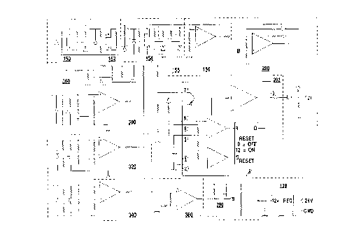
Reference is first made to Fig. 1 for a composite circuit diagram of the
controller governance circuitry of the present invention. Fig. 1 does not describe in
detail the specific Cu.~Jon(~ta of the various circuits of the present invention, but
rather describes the functional sub-circuits which go into the overall compositecircuit.
The governance circuitry of the present invention may be connected to a DC
motor controller circuit (not shown) at junction Jl. Junction Jl is the output for
power level transition circuit (280), as well as the output for the controlled power
limiting function seen through pulse width modulator circuit (202). Power level
transitlon circuit (280) controls the rate at which a voltage is brought to a level
indicative of the speed selected by the vehicle operator. Circuit (280) also controls
WO 92/15147 C A 2 1 1 7 5 4 9 P~r/usgVol352
the ratc of decrease in velocity when a lower speed is selected by the operator.Power level transition circuit (280) also receives a signal from power initiation reset
circuit (390) that indicates controlled power limiting activity has ceased, and the
vehicle may then power up from a zero velocity state. Power level transition circuit
(280) receives this signal from power initiation reset circuit (390) via connection B.
Power level transition circuit (280) receives the power level (speed) selected
bytheoperatorfrompowcrlevcladdercircuit(l56). Powerleveladdercircuit(156)
cumulates the effects brought about by a selection on the external controls of the
vehicle, through power level select circuits (150, (152), and (154) and adder biasing
circuit (155). In the preferred cmbod t, this group of three power levél select
circuits incorporate low power circuit (150), medium power circult (152), and high
power circuit (154), Typically, low power incorporates only the functioning of low
power circuit (150), medium power results from the cumulative effect of activating
both low power circuit (150), and medium power circuit (152), and high power is the
cumulative effect of all three power level select circuits. Adder biasing circuit (155)
provide a baseline voltage to which circuits (150, (152), and (154) add to.
The controlled power limiting function of the present invention is achieved
primarily by pulse width modulation circuit (202). The functional output of pulse
width m~)d~ t circuit (202) is a pulsed waveform of a duration appropriate for
the gradual decrease in the power level Or the vehicle. Pulse width modulation
circuit (202) is started by a signal from comparator circuit (380). Comparator circuit
(380) is controlled by a plurality of controlled power limiting event circuits (300),
(320), (340), and (360). In a preferred ~mbotl t forward circuit (300) is engaged
when the powered vehicle is in the forward configuration and a forward solenoid
(not shown) is active. Reverse circuit (320) is engaged when the powered vehicle is
in reverse, and a reverse solenoid (not shown) is active. Power limitation circuit
(340) is engaged when there is an overpower condition in the motor that requires a
controlled power. Safety switch circuit (360) incorporates a means for over riding
wo g2/15147 C A 2 1 7 5 4 ~ PCT/US92/013S2
circuits (300, (320), and (340), so as to prcserve the original safety functions present
in the vehicle.
The specifics of each of the above referenced sub-circuits are described in
more detail below. One additional circuit not mentioned above but indicated in Fig.
1 is voltage governance circuit (139) that provides the operational 12 volts DC that
the controller circuit and the circuitry of the present invention require from atypical DC battery that most electric vehicles use to function. The controller
circuitry and the go~e.l.ane., circuitry of the present invention may typically be
used with batteries ranging from 6 volts to 600 volts with operational voltages in the
range of 3 volts to 120 volts.
Power Level Select Circuitry
The power level input of a typical solid state DC controller is provided with
a voltage from power level transition circuit (280) that under ordinary circumstances
is d.,ic. ~ -' by the power level select circuitry shown in Fig. 2. The power level
select circuitry is comprised of low power circuit (150), medium power circuit (152),
high power circuit (154), adder biasing circuit (155), and power level adder circuit
(156).
Power level circuits (150), (152), and (154) are in VlOg-caai~ combination
provided with the battery voltage of the powered device at (160), (170), or (180),
according to the power level selected by the vehicle operator. Diodes (162), (172),
and (182) serve as spike a~ lcaaOIa for their respective circuits. When power level
circuits (150, (152), and (154) are not ~activated" by a battery voltage at (160, (170),
or (180) respectively, FET devices (167, (177), and (187) provide a steady statevoltage that in turn provides an "output~ voltage at points (169, (179), and (189),
equal to the voltage rating of zener diodes (168, (178), and (188). In the preferred
embodiment, these diodes are each 2VDC diodes. Adder biasing circuit (155)
provides a base voltage to which voltage from circuits (150, (152), and (154) are
WO92/15147 CA2 1 i 7549 ~ PCrt~lsg2/0l352
added. In the preferred ~mhod t, zener diode (194) maintains a base biasing
voltage at 6VDC at point 199. Pull up is provided by resister (191).
Thus, with no power level selected, the circuits (150, (152, (154), and (ISS),
provide 2VDC, 2VDC, 2VDC, and 6VDC ~ Li~,ly, to power level adder circuit
(156). This total of 12VDC equals the voltage at the positive input of adder (190),
as biased by resistor pair (192/193).
When the power level circuits (150), (152), and (154) are "activated" by a
battery voltage at (160), (170), or (180) respectively, the gates of FET devices It is
another object of the present invention to (164), (174), and (184) are provided with
a voltage divided by resistor pairs (161/163), (171/173), and (181/183). This voltage
switches FET devices (164), (174), and (184) into a conducting state, which provides
an "output" voltage at points (169), (179), and (189) equal to OVDC, In the preferred
~ ' t, therefore, the total voltage cumulated by adder (190) is 2VDC less for
each circuit (150, (152), and (154), that has been activated. This means that the
voltage seen at the negative input of adder (190) proceeds in step-wise fashion from
12VDC to 10VDC to 8VDC to 6VDC.
Inthepreferredemt~od t,resistors(l65),(175),(185,(195),and(197)(the
feedback for adder (190) are of equal value. Other well known solid state and non-
solid state switching devices could be utilized in place of FET devices (164/167),
(174/ 177), and (184/ 187).
Power level circuits (150), (152), (154), and adder biasing circuit (155)
together provide a specific selected voltage to power level adder circuit (156). This
voltage at the negative input of adder (190) is distinctive of high, medium, or low
power level selection, and is compared with the positive input voltage. The output
is the difference between these two input voltages. Operational adder (190) has a
positive input biased by resistor pair (192/193), wherein resistor (192) is tied to
+12VDC and resistor (193) is tied to ground. Operational adder (190) has feedback
resistor (197) and provides an output voltage through resistor (194).
WO 92/15147 PCT/US92/01352
CA21 1 7549
12
InthepreferredemhO~i ~,resistorpair(192/193)biasesthepositiveinput
of adder (190) to a 6VDC. The step-wise transition, therefore, of the negative of
adder (190) from 12VDC down to 6VDC, therefore results in an output from power
level adder circuit (156) that progresses in step-wise fashion from OVDC up to
6VDC, with OVDC indicating a full off condition, and 6VDC indicating a full on
condition. Thisstep-wisep.og.cs~;.,,ofvoltagefrompowerleveladdercircuit(156)
is then provided to power level transition circuit (280), which is described in more
detail below.
Controlled Power Limiting Circuitry
Reference is now made to Fig. 3 for a description of the circuitry which
determines when controlled power limiting should be initiated. Controlled power
limiting refers to the process of controlling the dccclcration of thc vchiclc during
a transition from a positive/forward direction to a ncgative/reverse direction, or
vice versa, by controllably reducing power before a switch over is madc. Controllcd
powcr limiting may also bc dcsigncd to occur when power limitation factors or other
cxternal factors on the vehiclc dcmand a rapid but controlled braking of the motor
and vehicle. Overpower is just such a limitation factor, and calls for controlled
power limiting when the drive motor circuit (not shown) is loaded in a manner that
draws too much powcr. This can occur if the vehicle encounters a significant
resistance to its forward or reverse motion. In the preferred embodiment there is
also a safety circuit that integrates the action of a "belly" switch into the controlled
power limiting function. The controlled power limiting circuitry works in
conjunction with power initiation reset circuitry (390) to achieve the controlled
transition appropriate to handle each of the above described situations.
Forward circuit (300), reverse circuit (320), and power limitation circuit
(340), are cach similar circuits whose characteristics may be adjusted, according to
the specific application that the circuit is intended for. In general, circuits (300).
WOg2/15l47 C A 2 1 1 7 5 4 9 PCT/US92/01352
(320), and (340), are designed to take resistors (317), (337), and (357), in and out of
a voltage dividing pair with resistor (383). This arrangement determines when
comparator (382) in comparator circuit (380) toggles. When the toggle occurs, this
is a signal to initiate controlled power limiting.
When the vehicle is in the forward configuration, the forward solenoid coil
is energized. This is sensed at terminal (303). Terminal (305) provides a connection
to the solenoid return and connects diode (306) which serves to suppress
voltage/current spikes generatcd in the solenoid coil. A high voltage (battery) is
thus seen at terminal (303), and is subsequently divided by resistors (307) and (308)
to energize the gate of field effect transistor (FET) (309). When energized, FET(309) provides a path to ground for resistor (311), which is connected to +12VDC.
Capacitor (313), which had previously been charged through resistors (311) and
(312), now discharges through resistor (312). It is important to notc that the
discharge time of capacitor (313) is less than the charge time. This means that when
a switch is made from activation of forward circuit (300) to activation of reverse
circuit (320), or vis versa, the second circuit comes on before the first circuit turns
off.
The negative input of comparator (302) is biased at a voltage determined by
resistor (314) and resistor (315). The output of comparator (302) is toggled high or
low to bring resistor (317) out of, or into, a voltage divider pair with resistor (383).
Comparator (302) is toggled low when the forward solenoid is energized, which puts
resistor (317) into circuit and provides a specific voltage to comparator (382) that
is above the toggle threshold of comparator (382).
When the vehicle is in the reverse configuration, the reverse solenoid coil ~s
energized. This is sensed at terminal (323). Terminal (325) provides a connection
to the solenoid return and connects diodc (326) which serves to suppress
voltage/current spikes generated in the solenoid coil. A high (battery) voltage is
thus seen at terminal (323), and is subsequently divided by resistors (327) and (328)
WO 92/15147 PCT/US92/01352
- CA2i l 754~
to energize the gate of field effect transistor (FET) (329). When energized, FET(329) provides a path to ground for resistor (331), which is connected to +12VDC.
Capacitor (333), which had previously been charged through resistors (331) and
(332), now discharges through resistor (332). It is important to note that the
discharge time of capacitor (333) is less than the charge time. This means that when
a switch is made from activation of reverse circuit (320) to activation of forward
circuit (300), or vis versa, the second circuit comes on before the first circuit turns
off.
The negative input of e , .,lo. (322) is biased at a voltage determined by
resistor (334) and resistor (335). The output of comparator (322) is toggled high or
low to bring resistor (337) out of, or into, a voltage divider pair with resistor (383).
Comparator (322) is toggled low when the reverse solenoid is energized, which puts
resistor (337) into circuit, and provides a specific voltage to comparator (382) that
is above the toggle threshold of ~; .,lu. (382).
Power limitation circuit (340) is connected so as to function somewhat
differently from forward circuit (300) and reverse circuit (320). In power limitation
circuit (340), a voltage is provided at terminal (343) with respect to common terminal
(345), that is across a shunt resistor (not shown) and is indicative of the current flow
in DC motor control circuit (not shown). In an overpower situation, a voltage
(0.25VDC in the preferred emhod l) is seen at terminal (343) which is normally
at OVDC. Diode (346) ensures the proper current flow in power limitation circuit(340). A non zero voltage at terminal (343), therefore, provides a voltage at the
negative input of comparator (342) by way of resistor (350) and RC pair (352/353).
This input causes comparator (342) to toggle low, which brings resistor (357) into a
voltage divider pair with resistor (383). This provides a specific voltage to the
negative input of comparator (382) that is below the toggle threshold of comparator
(382).
Safety circuit (360) is designed to sense when a "belly" switch has been
WO 92/15147 PCT/US92/01352
CA2i 1 7549 ,5
thrown on a "walkie" typc vehicle. A ~belly" switch (not shown) is a safety device
thatpreventsahand ~ at~dpoweredvehiclefrompinningtheoperatoragainst
a stationary object such as a wall. Such a switch is typically on the handle of
manually operated vehicles, and is a contact switch that engages the belly of the
operator when the operator is placed between the vehicle and a stationary object.
This ~ ~ ' t ~ly reverses the direction of the vehicle (by means not covered herein)
so as to prevent the operator from being pinned and being injured.
The "belly" switch circuit shown in Fig. 3 is capable of functioning with
either a switch that pulls junction (363) to high (the battery voltage of powered
device) or to ground. If the switch pulls (363) to high, a voltage divider pair made
up of resistors (367) and (368) provides a voltage to the gate of FET device (369).
The switching on of FET device (369) brings the 8ate of FET device (372) to ground,
which turns FET device (372) on, and shows a +12VDC to the negative input of
comparator (382). This voltage overrides any voltage created by the other controlled
power limiting event circuits, and ~ ' ~ly terminates the controlled power
function so as to allow the vehicle to reverse direction, and move out of the unsafe
situation without calling for controlled power, Resistor (370) is not used in the case
of a switch of junction (363) to hi8h-
If the safety switch (not shown) pulls point (363) to ground, then resistor
(370) is pulled into series with resistor (371), which provides a low voltage at the
gate of FET (372), which causes FET (372) to conduct and show a +12VDC to thc
negative input of comparator (382). Resistor (370) should have a low resistance in
this case. Resistors (367) and (368), and FET device (369) are not used.
When the vehicle is in motion either resistor (317) or resistor (337) is pulled
to ground. Resistor (317) and (337) are equal in the preferred embodiment. When
a second one of circuits (300), or (320) is engaged, which indicates a directional
motion change, then the corresponding resistor (317), or (337) is placed in a voltage
divider with resistor (383) in addition to the one resistor (317) or (337) already in
WO92/15147 CA21 17549 16 PCf/US92/01352
circuit. The combination of two parallel resistors to ground in circuit creates a
voltage at the negative input of comparator (382) which is below the toggle threshold
of comparator (382), which in turn initiates controlled power iimiting. When thevehicle is switched from forward to reverse, or vis versa, capacitors (313) and (333)
prevent the immediate release of rcsistors (317) or (337), as the case may be, long
enough for controlled power limiting to be initiated. Resistor (357) is half the value
of (317) or (337), and therefore, alone in circuit with resistor (383) produces a
voltage at the negative input of alul (382) that is below the threshold of
toggle; . ~to, (382) and triggers controlled power limiting. The controlled
power limiting circuitry is described in more detail below.
Comparator (382) is biased at its positive input by resistor pair (385/384) at
a voltage that controls the toggle of comparator (382) to occur above the point at
which resistors (317), and (337) have together been put into circuit with resistor
(383). Either of these resistors (317), or (337) by itself with resistor (383) is not
enough to cause comparator (382) to toggle.
Reference is now made to Fig. 4 for a dc,~ ion of the pulse width
modulation (PWM) circuitry of the present invention which receives the signal toinitiate controlled power limiting and produces the pulsed waveform output that
results in controlled power limiting. The output PWM circuit (202) is provided to
junction J I through diode (252). PWM circuit (202), is composed primarily of timer
circuit (200). Timer circuit (200) is an NE555 timer connected in a pulse width
modulator configuration with its reset terminal (4) driven by the output of
comparator circuit (380) through voltage divider pair (386/393). A PWM circuit
alternates between two unstable states, and creates a sequence of pulses at a desired
frequency and band width. This output of the NE555 circuit is then provided to the
controller circuitry (not shown).
PWM circuit (NE555) (200) is externally biased across terminals (7) and (6)
by resistor (214), is provided with +12VDC at terminal (8), has terminal (7) pulled
WO92/15147 C A 2 i 1 7 5 4 9 PCT/US92/01352
up to +12VDC through resistor (215), has a control voltage maintained by capacitor
(212) at terminal (5), has a voltage maintained at terminal (2) by capacitor (213), and
is grounded at terminal (1). The trigger at terminal (2) is connected to the discharge
terminal (7) by way Or resistor/diode pair (218/216), and is additionally tied to
threshold terminal (6). Appropriate biasing values may be chosen according to
standard NE555 timer specifications that will provide a PWM signal at the output(terminal (3)) that toggles low (an "onr motor condition) for anywhere from 0-5% of
the cycle and high (an ~off" motor condition) for the balance of the cycle.
Once the velocity of the vehicle has dropped to zero, the reset voltage
provided to PWM circuit (200) at its reset terminal (4) from circuit (380), again goes
low.
Power Initilltion Reset Circuitry
Reference is now made again to Fig. 3 for a description of the power
initiation reset circuitry of the present invention. Power initiation reset circuitry
(390) is comprised of capacitor (396), pull-up resistor (397), and FET device (398).
The RC combination (396/397) is designed not to alter the steady state conducting
characteristics of FET device (398) when a toggle of comparator (382) goes from low
to high, which initiates controlled power limiting. The RC pair (396/397) sends a
low voltage spike to the gate of FET device (398) when comparator (382) toggles
from high to low. This low voltage spike switches FET device (398) into a
momentary conductive state, which (via connection B) drives the positive input of
integrator (392) high long enough to reset its output, and allow for the controlled re-
acceleration of the motor from a zero velocity state.
Power Le-~el Transition Circuitry
Reference is now made to Fig. 5 for a description of the power level
transition circuitry, and the means whereby the voltages presented by the various
WO 92/15147 C A 2 i 1 7 5 4 ~ PCT/US92/01352
18
ancillary circuits described above are incorporated into a single input into the DC
motor control circuitry (not shown). The core of power level transition circuitry
(280) is integrator (392). Intcgrator (392) is provided a voltage signal from the power
levcl adder circuit (156) at its negative input through junction D. Thc positivc input
of integrator (392) is ordinarily biased by resistor pair (395/394). Whcn powcr
initiation reset circuit (390) activates its - y low voltage spikc the positive
input of integrator (392) is made to go high long enough to rcset the power level to
zero and restart the powcr level transition curve.
Thc slopes of thc positive and negative power Icvel transition curves~ are
d~ i-.cd by the characteristics of the resistors and capacitors in the feedback loop
for integrator (392). The values for capacitor (254) and resistors (256) and (260) are
selected so as to providc a controlled voltage change at the output of integrator (392)
in response to the input voltage from power Icvel sclcct circuitry (156). Diodes (258)
and (262) ensure that the proper resistor is in circuit for either a positive power level
transition (a.. ~,lc, ) or a negativc transition (deceleration). This allows for an
acceleration rate distinct from thc dcceleration rate. The output of integrator (392)
is thcn provided to junction Jl through diode (250), and provides the control
circuitry (not shown) an analog voltage indicative of the power level selected.
The controlled power limiting function itself, as mentioned above, is scen
dircctly at junction Jl from the output of PWMcircuit (202). Diode (252) is in line
with PWM circuit (202) through to junction C. The output through diode (252)
interacts with the output through diode (250) such that the higher analog voltage
signal is passed to junction Jl. That is, when the controlled power limiting function
is not operating and the output through diode (252) is low, junction Jl sees only the
analog voltage output through diode (250) from power level transition circuit (280).
When a controlled power limiting function is operating, then the waveform at diode
(252) is a pulsed waveform that alternates between a short band width low state, and
a large band width high state. This waveform is affected by the analog voltage levcl
C A 2 1 1 7 5 4 9 PCT/US92/01352
19
through diode (250). The analog voltage level through diode (250) serves to prevent
the low section of the pulsed wavcform through diode (252) from dropping below
a value indicative of the power level selected. This ensures that the controlledpower limiting signal does not ignore the power level selected at the time controlled
power limiting is initiated. In other words, if the power level selected is already
low, the controlled power limiting signal incorporates this low power level into its
pulsed waveform signal. Likewise, if the power selected is high, the controlled
power limiting signal incorporates this high power level in its pulsed waveform. The
effect is seen more clearly in Figs. 6 through 9 discussed below.
Fig. 6 is a graphic representation of the analog output at Jl from the
circuitry of the present invention when the powered device is in a normal, partial
power, functional configuration. This voltage is seen when a relatively low power
has been selected by the operator. This low power is reflected by a voltage that is
closer to SVDC (full off) than to OVDC (full on), and is shown as constant afterhaving been brought up gradually by power level transition circuit (280). A higher
power level would be indicated by a lower constant voltage at junction J 1.
Fig. 7 is a PWM waveform present in the type of-solid state DC motor
controlier typically associated with the present invention, in response to a voltage
signal such as that seen in Fig. 6 at Jl. The analog voltage signal from the circuitry
of the present invention is translated into a pulsed waveform in a typical DC control
circuit, whose band width at the battery voltage level is inversely proportional to thc
voltage level provided by the governance circuitry at Jl. Thus, a voltage level on
the order of that shown in Fig. 6 will result in a pulsed waveform in a typical solid
state DC motor controller circuit whose positive band widths proportionately reflect
the analog voltage level.
When controlled power limiting is initiated, as described above, the
governance circuitry of the present invention provides a voltage signal similar to
that shown in Fig. 8. This voltage signal is a pulsed waveform that provides a 5VDC
WO 92/15147 PCT/US92/01352
~ A~ 1 1 7 54~
value at ~1 for a majority of the cycle time, and an analog voltage level (determined
by the power level select circuitry) for a very small portion of the cycle. Thisreduces power to the motor without a sudden drop to zero power, and a sudden
shutdown of the vehicle. The result, after this controlled power limiting signal is
translated in a typical DC motor controller circuit, is shown by the waveform in Fig.
9. Therein, the pulsed waveform of Fig. 7 is ~passed~ only during the non-5VDC
window determined by the controlled power limiting circuitry. The MOSFET, SCR,
or other switching devices which see the voltagc waveform shown in Fig. 9,
therefore, are conductive only during the windows created by the controlled power
limiting circuitry. During these windows, the pulsed waveform is the same as that
determined as before controlled power limiting by the power level selected. Thus.
controlled power limiting allows for a dynamic decrease from any power level
selected in the power level select circuitry, and prevents sudden changes in direction
or overpower
Although the invention has been described with reference to a specific
bo~1 t, this d.,a.,.i,u~ion is not meant to be construed in a limiting sense.
Various modifications of the disclosed embodiment, as well as alternative
embodiments of the invention, will become apparent to persons skilled in the artupon reference to the description of the present invention. Any powered device
which could benefit from the governing functions provided by the present invention
would easily incorporate the circuitry of the present invention. As described above,
the application of the present invention to other means for delivering power to a
power consuming device, are simply analogous to the d,a~ ,tiu.., of the application
of the present invention to the control in the preferred embodiment. It is therefore
contemplated that the appended claims will cover such other applications that fall
within the true scope of the invention.