Note: Descriptions are shown in the official language in which they were submitted.
21 17 9 3 6 ~.~
_1_ _ _
LOGIC CIRCUIT HAVING ERROR DETECTION FUNCTION, REDUNDANT
RESOURCE MANAGEMENT METHOD, AND FAULT TOLERANT SYSTEM USING IT
BACKGROUND AND SUMMARY OF THE INVENTION
The present invention relates to a self-checking circuit
and its configuration. More particularly, it concerns a self-
checking circuit useful for highly reliable system
configuration.
The present invention also relates to a management method
of a redundant resource, and, more particularly, concerns an
effective use of the redundant resource in a fault tolerant
computer system.
Control systems for airplanes, trains, automobiles, and
similar means of transportation are increasingly electrified
as advanced control performances are needed to increase the
energy (fuel) efficiency, the operability, the comfort, and
speed. To run the means of transportation safely, any of the
control systems is required to be high in reliability and
fail-safe performance such that no dangerous output or result
is caused by the occurrence of a fault.
To assure the reliability and fail-safe performance of a
control system, it is important for the control system to have
a capability of detecting the occurrence of a fault, that is,
a self-checking capability. To accomplish this self-checking
capability, the so-called redundant code is generally used
that has a hamming distance of higher than 2 between codes,
such as the M-out-of-N code and the two-rail logic (1-out-of-2
code) that can be regarded as a kind of M-out-of-N code. The
redundant code can perfectly detect a fault as long as it is a
single fault. However, it cannot always detect a multiple of
21 17~3fi
-2-
faults. If the self-checking circuit is accomplished in an
LSI, the fault may spread over the whole chip. This would be
a phenomenon equivalent to the occurrence of multiple faults.
Assuming the errors are random, Eq. 1 below gives the
probability r~ of wrong output signals due to a fault
coinciding with code points in a specific output code space O.
rj - No/Nu .........................................(1)
where No is the number of the code points in the output code
space O and Nu is the number of the code points. Therefore,
it is a problem how to increase Nu to No to increase the
detection rate.
There are the following two methods of accomplishing a
self-checking circuit having such redundant codes as described
above.
(1) A method of forming the whole circuit of redundant
codes.
(2) A method of replicating function blocks and using a
self-checking comparison circuit formed of redundant codes to
compare signals output of the function blocks.
Method (1) above has the problems that the circuit must
be newly designed to achieve self-checking and it is difficult
to optimize its operational speed.
On the other hand, method (2) has the advantage that the
usual processor, memory, and other devices can be used for the
function blocks, since only the comparison circuit need be
newly designed in redundant logic. This can decrease the
development cost to a great extent. It also can easily make
the operational speed high, since advanced semiconductor
21 17936 -:
- 3 _ _.
techniques can be used. The self-checking coverage of method
(2) greatly depends on that of the comparator.
Accordingly, to accomplish a self-checking comparator, it
has been proposed to use redundant codes, such as the M-out-
of-N code and two-rail logic (1-out-of-2 code), for the logic
itself used in the comparison circuit. See, for example,
Yoshihiro Toma, "Theory of Fault Tolerant System", Association
of Electronics, Information and Communications, 1990. To
accomplish a self-checking comparator, they connected the RCCO
(Reduction Circuit for Checker Output) circuit shown in Fig.
2.5 on page 31 to a tree structure as shown in Fig. 2.6 on
page 32.
The probability of a fault occurring in the circuits to
be compared is low. It is therefore rare that the signals to
be compared do not coincide. This means that it is rare that
a path to be activated upon detection of the inequality is
activated. If there occurs such a type of fault as fixing so
that the signal output of the path always means 'equality',
the fault may be made latent. The comparison circuit,
therefore, does not only use the redundant code described
above, but also uses a frequency logic, alternating checking
method, or similar dynamic logics of alternating signal
levels, as a signal indicating that the circuit is normal
(hereinafter referred to as the signature signal), in place of
the binary level logic of 0 and 1. As an example, we can use
a method of repositioning a permuter for injecting a simulated
fault for testing into the RCCO shown in Figs. 2.15 and 5.16
on page 42 in the above mentioned "Theory of Fault Tolerant
- . 21 179 3 6
-4- -
System". With this method, an alternating output signal is
obtained if the operation is normal. The alternating output
signal is not obtained, on the other hand, if a fault is
caused by a change of a threshold value of a semiconductor
device or a fault is due to a change of a do characteristic of
the device, such as a failure stacked at 0 or 1. The method
also injects the simulated fault periodically to always
confirm operation of the error detection feature. These
advantages can make the circuit increase the self-checking
performance to a great extent.
The above-described prior art has the disadvantage that
the adverse effect of crosstalk or shortcircuit between wiring
nets in the semiconductor device likely occurs. If a fault of
the semiconductor device causes crosstalk between the wiring
nets or shortcircuiting between the wiring nets, or if
migration of a wiring material or poor insulation between
insulation layers causes a shortcircuit, the wiring net that
should have no signature signal in itself may have a signature
signal of another wiring net adversely induced thereinto
(hereinafter referred to as a counterfeit signature). In
general, the fail-safe circuit has a signature signal to
indicate that the circuit is normal. The circuit may
recognize that it is normal in spite of a counterfeit
signature due to crosstalk or a shortcircuit. It is feared
that the fail-safe performance of the circuit is then lost.
To prevent such an occurrence of crosstalk and
shortcircuiting, the prior art has a special design
restriction in the wiring spaces. However, this method has to
21 17936
-5-
form transistors and wiring lines on the semiconductor
substrate on the basis of restrictions quite different from
the general semiconductors. It cannot have any of the
convenience of the prior art and automatic designing tools.
Most of the designing works must be done manually.
Further, computers and transportation controls bear
central roles for finance and similar social key industries
and parts involved in human life in controlling spaceships and
airplanes in recent years. A system breakdown or wrong system
operation due to a fault in the computers can have fatal
effects in society. Consequently, high reliability of the
computers is increasingly needed.
To make the computers reliable, there is generally
adopted means of redundancy produced by providing extra
computers and units forming the computers in advance.
On the other hand, the redundant hardware to make the
computers highly reliable results in a great increase of
costs, dimensions, weight and power consumption. To enhance
the investment effect or the cost performance of the fault
tolerant computer system, it is necessary to increase the
redundant hardware resource effectively with respect to the
reliability and processing performance.
There is a method of redundant resource management to use
the redundant hardware resource. That is proposed by Jean-
Charles Fabre, et al., "Saturation: reduced idleness for
improved fault-tolerance", Proc. FTCS-18 (The 18th Int'1 Symp.
on Fault-tolerant Computing), pp. 200-205, 1988.
21 17936 .
-6-
This prior art by Jean-Charles Fabre, et al., has MNC
(minimum number of copies), or redundant copies, provided in
advance to be simultaneously executed for each of the tasks.
If the number of idle nodes (redundant computer modules) is
larger than the MNC at the time of arrival of a task execution
request, the idle nodes start execution of the task. If the
number of idle nodes is smaller than the MNC, the system waits
until the current execution of the tasks has ended to provide
the required number of idle nodes.
This prior art by Jean-Charles Fabre, et al., is a useful
method of redundant resource management for an OLTP (online
transaction processor) that has a task start request made
frequently.
However, this prior art lacks sufficient consideration of
the occurrence of a fault and the further occurrence of
multiple faults to make highly reliable the real time control
computer. This is due to the fact that the proposed prior art
is based on the assumption that the task execution time is
sufficiently shorter than the MTBF (mean time between
failures) with respect to the operational characteristic of
the OLTP that the transaction ends in a short time. However,
the real time control computer often has tasks executed for a
long period of time. The computer of an airplane, spaceship,
etc., for example, must not only run for the mission time
normally, but also must support a halting of the mission. For
this reason, the task execution time cannot be ignored as
compared with the MTBF. We must take into account the
~1 179 3 6
occurrence of a fault and the further occurrence of multiple
faults .
The above-described prior art has the number of assigned
computer modules managed only at the time of starting of the
task execution. Therefore, no computer modules are newly
added, even if the task executing computer module is caused to
fail to function by the occurrence of a fault during execution
of the task. This means that, if the fault occurs during
execution of a task, this is continued while the degree of
redundance is decreased, that is the number of computer
modules that are redundantly executing the task. The
reliability of the task is lost. If one of two computer
modules redundantly executing a task fails to function, for
example, should a second fault occur simultaneously, execution
of the task is halted.
A first advantage of the present invention consists in
the fact that a logic circuit having an error detection
function with blocks that feed out a plurality of duplexed
signals, compares the output signals of the function blocks
and detects an error on the basis of the results of the
comparison, the circuit comprising synthesizing means provided
to superimpose inherent waveforms assigned in advance to the
respective output signals of the function blocks onto the
output signals of one of the function blocks, and comparison
means for comparing a signal output of the synthesizing means
with a signal output of another function block to detect the
error.
z~ ~~93s
_8_
For a semiconductor device, as an example, an inherent
signal waveform is assigned to each of the wiring nets
corresponding to the above-mentioned output signals as a
signature. The signature should be regarded as authentic only
if the signal waveform coincides with the one inherent in the
wiring net.
To distinguish an authentic signature from a counterfeit
signature, it is desirable to make the signatures inherent in
the wiring nets not correlate with one another. Orthogonal
functions are well known not to correlate with one another.
Functions fi(x) and fj(x) are orthogonal to each other when
f ~fi (x) ~fj (x) dx = 0 eq. 2
The wavelet analysis that can analyze a signal waveform
in a time-frequency domain has recently been noted in place of
the conventional Fourier analysis. The original wavelet also
is an orthogonal function. A triangular function and a
wavelet are analog functions. To use these in a digital
circuit, they should be made binary.
V~lith the first feature of the present invention, for a
semiconductor device, as an example, the inherent signal
waveform is assigned to each of the wiring nets as the
signature. The signature should be regarded as authentic only
if the signal waveform coincides with the one inherent to the
wiring net. If a fault of the semiconductor device causes
crosstalk between the wiring nets or if migration of wiring
21 17936
-9-
material or poor insulation between insulation layers causes a
shortcircuit, the wiring net may have a counterfeit signature
signal of another wiring net adversely induced thereinto.
Should this happen, the counterfeit signature can be
distinguished from the authentic signature, since the
counterfeit signature does not coincide with the signal
waveform inherent in the wiring net. This means that the
present invention needs no special wiring restrictions to
prevent crosstalk or shortcircuiting that are indispensable to
the prior art methods of fully detecting faults. In addition,
the present invention assures fail-safe performance.
The effectiveness of the conventional technology is based
on the presumption that the fault detected in either of the at
least dualized function blocks is independent of the other
function block. In other words, it is premised that the same
fault never occurs in both of dualized function blocks at the
same time. If the same fault does occur in both of the
dualized function blocks at the same time, the fault outputs
from both of these blocks match and it becomes impossible to
detect the fault by comparing them. This becomes a big
problem when dualized function blocks are arranged in the same
semiconductor chip. Such problem can be solved by providing
the following control methods according to the invention.
The following means that is called diversity may be taken
to guarantee the independence of faults to occur in either of
the dualized function blocks.
(1) Design diversity
-lo- 21 17 9 3 fi
The design diversity is an effective means to eliminate
the influence of faults caused by design. Especially,
N-Version Programming for software is well known. The
N-Version Programming is a method to execute N versions of a
program that are developed with the same specifications
concurrently. Also, in the case of hardware, this design
diversity can be achieved by developing circuits with the same
specifications in N ways. According to this method, however,
the number of processes and the expense need to be by N times
that of an ordinary method for the design and development.
Thus, this method is not effective.
To reduce the number of processes and the expense in
designing hardware, therefore, the following method is
provided in this invention.
The main current to design modern hardware uses the HDL
(Hardware Description Language) to create a file (logical
description) that describes the functions and specifications
of the subject logical circuits, and creates another file
(logical net list) that describes the connections of the
logical circuits using a logical synthesis tool on the basis
of the HDL. In addition, the logical net list file is
converted to a physical net list file that describes the
wiring and layout of transistors on the actual semiconductor
chip using an auto wiring tool to create the necessary masks
and the semiconductor elements.
In this case, the design constraints, such as the delay
time, occupation area, etc., as well as the subject algorithm
..... 21 17 9 3 fi
-11-
can be changed for logical synthesis and automatic wiring to
diversify the target logical net list and physical net list.
The dualized function blocks can thus be achieved in the
subject semiconductor chip on the basis of the logical
description of the logical blocks by selecting two physical
net lists from among the diversified plural physical net
lists.
To select two physical net lists from among many, it is
only necessary to define a correlation function that indicates
how much those physical net lists resemble each other and
select a combination of the physical net lists such that the
correlation function can be minimized. In this case, the
fault characteristics of the semiconductor must be affected in
the correlation function. In general, a wire intersection is
a weak point of semiconductors. At a wire intersection, two
wires are separated only by a thin film oxide, so
shortcircuits between wires and shorts, such as crosstalk,
etc., are apt to occur. Furthermore, since one wire crosses
over another at such a wire intersection, the wire located at
a different level is often cut by stress. In other words, the
status of the intersection between wires affects the fault
characteristics of semiconductors. The correlation function
in which the fault characteristics of the semiconductor is
affected can thus be defined as follows.
[Formula 1]
m n
~klk2 ~ ~, ~ijkl~ ~jik2 2Cj. 1
i=1 j=1
21 17936
-12-
However, the ~;~k must indicate whether an intersection
exists between wiring nets and be defined as follows.
[Formula 2]
O:no wiring netsiJ intersecting
1: wiring netsl~ intersecting
(2) Time diversity
A fault that occurs in either of dualized function blocks
due to electric noise, etc. can be prevented from affecting
the other, even when they are designed in the same way, by
individually delaying the timing of their operation. To
achieve such a time diversity, the clock or input signal that
decides the timing of a dualized function block operation is
entered into only one of the dualized function blocks through
a delay circuit. When comparing the output signals from those
function blocks, the signal from the other function block can
be output through the delay circuit to compare it with that of
the former function block in the comparison circuit.
(3) Space diversity
When separating one of the dualized function blocks from
the other, it becomes possible to prevent a temporary fault
that occurs in either of those function blocks due to
electrical noise, cosmic rays, radiation, etc., as well as due
to damage of the subject semi-conductor chip from affecting
the other. When a function block is dualized in a chip and
each is checked by itself, the dualized function blocks should
be arranged in the same direction and in the same pattern.
With this arrangement, the effectiveness of the space
~1 179 3 6 -~
-13- _
diversity is maximized. The corresponding sections of the
dualized function blocks can therefore have the same distance.
As a result, it can be avoided that the corresponding sections
of the dualized function blocks come excessively close to each
other to deteriorate the effectiveness of the space diversity.
According to this invention, the design diversity, the
time diversity, and the space diversity can guarantee the
independence of faults detected in any of the dualized
function blocks by comparing the outputs from both the
function blocks. With this, it is avoided that the same type
faults occur at the same time with a correlation in both the
dualized function blocks. It also becomes possible to detect
faults by comparing the outputs from those function blocks.
A second advantage of the present invention consists in
the fact that a distributed fault tolerant system having a
plurality of computer modules assigned to execute a plurality
of tasks, comprises selection and execution means that, if a
fault occurs in any of the computer modules of the system,
selects at least one of the computer modules having tasks
assigned thereto other than the task that the broken computer
module, and assigns to the selected computer module the task
that the broken computer module has executed, and makes the
selected computer module execute the task.
Each of the computer modules operates as follows:
(1) The computer module broadcasts its fault occurrence
information (fault detection results) and process results to
the other computer modules with proper timing (check points)
during processing the task.
21 179 3 6
-14-
(2) The computer modules calculate their respective
evaluation functions Fij, where i is a processor number and j
is a task number. The evaluation function Fij can be regarded
as a margin for the responsibility to be taken on by the
computer module for the task. It is based on the equality or
inequality of the fault occurrence information (fault
detection results) and the process results broadcast from the
other computer modules.
(3) Each of the computer modules decides task j for
minimizing the evaluation function Fij as a process to execute
before switching the task in process to the next process to be
executed.
The evaluation function Fij represents the margin of
reliability of the task. Therefore, it should be determined
that Fij can be as low as the importance of the task is high,
Fij can be as low as the responsibility of the computer module
for the task is high, and Fij can be as high as the
reliability of the task is high.
An example of the evaluation function Fij meeting these
conditions is
Fij - Lrj - Lthij, or
Fij - Lrj / Lthij
where Lthij is a threshold value of the reliability level
of task j in the computer module i, Lrj is the reliability
level of task j, i is the individual computer module number,
and j is the task number.
Another example of the evaluation function Fij meeting
the conditions above is:
-15- 21 17 9 3 6
Fij - log{(1-Lthij)/Pej}
where Pej is the probability of wrong calculation results
of task j.
It should be noted that Lthij, which is the threshold
value of the reliability level of task j, is different
depending on the importance of the task. It is set to a high
value if the task is needed to have a high importance or a
high reliability.
Further, Lthij has to be different depending on the
computer module. It has to be as high as the responsibility
of the computer module is high for the task.
With the second feature of the present invention, the
computer modules are assigned to the tasks so that the
evaluation functions Fij can be made always to balance. This
will not make Fij of a specific task jut out too high or too
low. That is, if there is a specific task of low reliability
level (hereinafter referred to as an endangered task) due to
the occurrence of a fault during operation, a computer module
executing another task having a margin of reliability is made
to execute the endangered task. This can prevent the
reliability level of the specific task alone from being
lowered. For this reason, the second feature can be a
countermeasure against any occurrence of a fault during the
execution of the tasks, so that the responsibility given to
the system can be fulfilled while the reliability is
maintained.
Also, since Lthij is set high as the importance of the
task is high, Fij can be balanced with the other tasks of
21 17936
-16-
higher Lrj. For this reason, a number of computer modules
should be assigned to much of the task, the importance of which
is high, to keep the higher reliability level Lrj.
Further, since each of the computer modules can
autonomously decide the task to execute, it is necessary to
have a central arrangement for assigning task executions,
thereby avoiding single fault points. This means that a single
fault will not affect the whole system, hence increasing the
system reliability.
BRIEF DESCRIPTION OF THE DRAWINGS
The above and other objects, features and advantages of
the present invention will be apparent from the following
detailed description of the preferred embodiments of the
invention in conjunction with the accompanying drawings, in
which:
Fig. 1 depicts a circuit diagram illustrating a basic
embodiment of the present invention;
Fig. 2 depicts a circuit diagram illustrating an
embodiment corresponding to function blocks;
Fig. 3 depicts a circuit diagram illustrating an
embodiment of the present invention having a comparator formed
of the RCCO tree;
Fig. 4 depicts a circuit diagram illustrating an
embodiment of the present invention in which signals fed from a
function block also have an orthogonal waveform added thereto;
Fig. 5 depicts a circuit diagram illustrating an
embodiment of the present invention in which orthogonal
waveform generating circuits are duplexed;
21 17936
-1~-
Fig. 6 depicts a signal timing chart illustrating the
orthogonal function waveforms;
Fig. 7 depicts a circuit diagram illustrating an
embodiment of the orthogonal waveform generator circuit;
Fig. 8 depicts a block diagram illustrating an embodiment
of an integrator circuit;
Fig. 9 depicts a timing chart illustrating the orthogonal
function waveforms and a signature output signal;
Fig. 10 depicts a timing chart illustrating the
orthogonal function waveforms and a signature output signal at
the time of a fault;
Fig. 11 depicts a block diagram illustrating an
embodiment of another integrator circuit;
Fig. 12 depicts another timing chart illustrating the
orthogonal function waveforms and a signature output signal at
the time of a fault;
Fig. 13 depicts a block diagram illustrating an
embodiment of another integrator circuit;
Fig. 14 depicts another timing chart illustrating the
orthogonal function waveforms and a signature output signal;
Fig. 15 depicts a detailed circuit diagram illustrating
an embodiment of the present invention;
Fig. 16 depicts a block diagram illustrating a self-
checking computer made according to an embodiment of the
present invention;
Fig. 17 depicts a block diagram illustrating a fault
tolerant computer functioning as a self-checking computer;
21 17936
-18-
Fig. 18 depicts a block diagram illustrating a switching
control circuit;
Fig. 19 depicts a circuit diagram illustrating a self-
checking comparator according to an embodiment of the present
invention;
Fig. 20 depicts a block diagram illustrating the
configuration of a fault tolerant system according to an
embodiment of the present invention;
Fig. 21 depicts a conceptually functional outline
illustrating a configuration of a computer module according to
an embodiment of the present invention;
Fig. 22 depicts a conceptually functional outline
illustrating another configuration of a computer module
according to an embodiment of the present invention;
Fig. 23 depicts a conceptual outline illustrating an
embodiment of the present invention;
Fig. 24 depicts a conceptual outline illustrating another
embodiment of the present invention;
Fig. 25 depicts a conceptual outline illustrating another
embodiment of the present invention;
Fig. 26 depicts a flow chart illustrating condition
judgement features that decide a task to be executed;
Fig. 27 depicts a timing chart illustrating instances of
switching a task;
Fig. 28 depicts a flow chart illustrating condition
judgement features having a dead-zone that decide a task to be
executed;
-19- 21 17 9 3 6
Fig. 29 depicts a timing chart illustrating a change of
Fij without a dead-zone;
Fig. 30 depicts a timing chart illustrating a change of
Fij with a dead-zone;
Fig. 31 depicts a graph illustrating the number of normal
computer modules assigned over time;
Fig. 32 depicts a block diagram illustrating an
embodiment of averaging Lrj;
Fig. 33 depicts a timing chart illustrating a change of
Fij without averaging Lrj;
Fig. 34 depicts a timing chart illustrating a change of
Fij with averaging Lrj;
Fig. 35 depicts a timing diagram illustrating an
embodiment of the present invention for reducing increases of
the amount of communications among the computer modules;
Fig. 36 depicts a flow chart illustrating a judgement
whether or not broadcasting should be made;
Fig. 37 depicts a flow chart illustrating another
judgement whether or not broadcasting should be made;
Fig. 38 depicts a block diagram illustrating an
embodiment of the present invention for application to an
adaptive-control system;
Fig. 39 depicts a table illustrating how the computer
modules are assigned;
Fig. 40 depicts a cross-sectioned view illustrating a
servo-motor system as an embodiment of the present invention;
Fig. 41 depicts a longitudinally sectioned view taken
along A-A' in Fig. 40 illustrating the servo-motor system;
Z1 17936
-20-
Fig. 42 depicts a circuit diagram illustrating a circuit
for the servo-motor system;
Fig. 43 depicts a block diagram illustrating a system
configuration in use for the servo-motor system;
Fig. 44 is a design automation by an automatic logical
synthesis tool and an automatic wiring tool;
Fig. 45 is a diversified design by diversifying
constraints;
Fig. 46 is an example of extracting some design results
from diversified design results;
Fig. 47 is an example of diversifying an operation time;
Fig. 48 is another example of diversifying an operation
time;
Fig. 49 is still another example of diversifying an
operation time; and
Fig. 50 is an embodiment of a layout in a chip.
DETAILED DESCRIPTION OF THE PREFERRED EMBODIMENTS
The embodiments of the invention will be set forth in
detail with reference to the accompanying figures and in the
following three sections of (1) Self-checking logic, (2)
Redundancy resource management, and (3) Diversities.
1. Self-checking logic
The following describes in detail self-check comparators
that are embodiments according to the present invention, by
reference to Figs. 1 to 19.
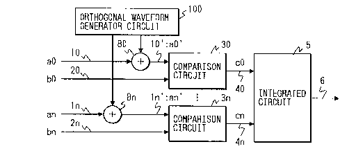
Fig. 1 depicts a circuit diagram illustrating a comparator
that is an embodiment of the present invention. In operation,
signals a0 to an (10 to ln) fed from a function block A have
errors injected thereinto for testing by
-21- 21 17 9 3 6
permuters 80 to 8n according to an orthogonal waveform (test
pattern) generated by an orthogonal waveform generator circuit
100. The signals having the errors become error-injected
signals a0' to an' (10' to ln'). Note that the permuters 80
to 8n, as shown in the figure, are exclusive-ORes that each
has a feature capable of injection of pseudo-errors for
testing. In turn, the error-injected signals 10' to ln' are
compared with signals b0 to bn (20 to 2n) fed from a function
block B (figure 2) by comparison circuits 30 to 3n.
Comparison results 40 to 4n are collected in a integrator
circuit 5. The integrator circuit 5 can feed out a signature
signal of normality to a signature output 6 only when the
comparison results 40 to 4n are normal signatures.
Let ai' represent any one of the error-injected signals
a0' to an' (10' to ln'). Then,
ai' - ai~pi ..................................... (3)
where i is a signal number of 0 to n, pi is the
orthogonal waveform (test pattern) generated by the orthogonal
waveform generator circuit 100, and ~ is an operator for the
exclusive-Ones. Also let ci represent any one of the
comparison results c0 to cn (40 to 4n).
Then,
ci = ai'~bi
- ai'-'pi~bi .................................. (4)
If the function blocks A and B are normal, ai = bi.
Then, ai~bi = 0. Hence,
ci = pi ........................................ (5)
21 17936
-22-
Since any ones of pi with i being 1 to n are orthogonal
to each other, ci also is orthogonal with cj, where i is not
equal to j. Assuming ai and pi are statistically independent,
or orthogonal, ai and ai' are orthogonal to each other, and bi
and ai' also are orthogonal to each other. In addition to the
orthogonal waveforms, the group of waveforms include
correlated waveforms of ai with bi and pi with ci. In order
to prevent a counterfeit signature from being generated by the
crosstalk or the shortcircuit mentioned previously, the
circuit layout should be designed so as to separate the signal
ai from bi and the signal pi from ci physically. This will
keep generation of a counterfeit signature due to crosstalk or
shortcircuiting from affecting the function. An embodiment of
the circuit layout will be discussed later by referring to
Fig. 15.
The embodiment of the present invention described above
can provide a fully self-checking comparator without any
special wiring limit.
The function blocks A 110 and B 111 shown in Fig. 2 do
not always feed out the effective signals a0 to an (10 to ln)
and b0 to bn (20 to 2n), but often feed them out together with
strobe signals that indicate that the signals a0 to an (10 to
ln) and b0 to bn (20 to 2n) are effective. In those cases, as
shown in Fig. 2, latch 120 and 121 should be held when the
strobe signals 130 and 131 make the signals a0 to an (10 to
ln) and b0 to bn (20 to 2n) effective. The kind of signals
used for the strobe signals in a circuit having a
microprocessor is different depending on the microprocessor.
21 179 3 6
-23-
The strobe signals available for an address signal and a
control signal include AS (address strobe) and BS (bus start),
and the ones for data signals are TA (transfer acknowledge)
and DTACK (data transfer acknowledge).
Fig. 3 depicts a circuit diagram illustrating an
embodiment of the present invention having a comparator formed
of the RCCO tree described in "Theory of Fault Tolerant
System," Yoshihiro Toma, Association of Electronics,
Information and Communications, 1990. In operation, signals
a0 to an (10 to ln) fed from the function block A have errors
injected thereinto for testing by the permuters 80 to 8n
according to the orthogonal waveform (test pattern) generated
by the orthogonal waveform generator circuit 100. The signals
having the errors become error-injected signals 10' to ln',
which are fed to the RCCO tree 3. Note that in the RCCO tree,
the signature output 6 also is of binary logic.
The RCCO tree 3, like the embodiment in Fig. 1, has input
and output signals made orthogonal therein to prevent a
shortcircuit from generating a counterfeit signature.
The embodiments given below are described on the basis of
the comparison circuit in Fig. 1. The comparison circuit of
the RCCO tree can be embodied in a similar way unless
otherwise specified.
Fig. 4 depicts a circuit diagram illustrating an
embodiment of the present invention in which signals b0 to bn
(20 to 2n) fed from a function block B have errors injected
thereinto by permuters 90 to 9n according to an orthogonal
waveform generated by an orthogonal waveform generator circuit
. . ..~ 21 17936
-24-
100. The embodiment can prevent a stack failure input to the
comparison circuit from becoming latent if bi is kept at the
same value for a long period of time. If bi is an address
signal and a program uses addresses in a specific area only,
for example, a high bit of the address is kept at the same
value for a long period of time.
Fig. 5 depicts a circuit diagram illustrating an
embodiment of the present invention in which the function
blocks A and B are associated with independent orthogonal
waveform generator circuits 100 and 101, respectively. This
embodiment having orthogonal waveform generator circuits 100
and 101 duplexed to detect and report any failures of the
orthogonal waveform generator circuits 100 and 101. The
embodiment also can make use of the superiority of the
independence of the two systems on the circuit layout that
will be discussed later by referring to Fig. 15.
Fig. 6 depicts a signal timing chart illustrating an
embodiment of the present invention that uses waveforms in
which pulses are turned on at time slots inherent to wiring
nets. The figure shows output patterns p0 to pn of the
orthogonal waveform generator circuit 100 and comparison
results c0 to cn (40 to 4n) when both the function blocks
A 110 and B 111 are normal.
Fig. 7 depicts a circuit diagram illustrating an
embodiment of the orthogonal waveform generator circuit 100
for generating the patterns as in Fig. 6. In operation, if
the system is power on to reset, a reset signal is made active
to preset a flip-flop 1001 to '1' as an initial value, then
21 179 3 6
-25-
resets flip-flops 1002 to 100m to '0' as an initial value.
That is, the train of flip-flops 1001 to 100m are set to 1, 0,
0, 0, 0, ..., and 0. After the power-on resetting, a CLK
(clock) signal successively shifts the pattern 1, 0, 0, 0, 0,
..., and 0 to generate the pattern in Fig. 6. The flip-flops
1001 to 100m are made redundant and majority outputs of each
of the redundant flip-flops are taken. This can prevent
software errors of the flip-flops due to noise and
radioactivity and temporary errors, such as a transient fault,
called single event upsets. It also can increase the
reliability. Of course, the orthogonal waveform generator
circuit 100 also can be used in the RCCO tree 3 in Fig. 3.
Fig. 8 depicts a block diagram illustrating an embodiment
of an integrator circuit 5 useful for the pattern in Fig. 6.
Such a simple OR gate as in Fig. 8 can make different
waveforms of the patterns in Fig. 6. This allows us to know
the occurrence of failure. Even if shortcircuiting occurs
among the wiring nets, an authentic signature will not wrongly
appear on the signature output 6, or no counterfeit signature
can be fed out, because there are no other wiring nets that
use the authentic signature for p2 and c2. This means that
even if a counterfeit signature is generated by a
shortcircuit, the embodiment can assure of fail-safe
performance.
Fig. 11 depicts a block diagram illustrating an
embodiment of the present invention that has an excess pulse
detection feature in addition to the pulse extraction
detection feature of the integrator circuit in Fig. 8. The
21 179 3 6
-26-
excess pulse is defined here as a phenomenon that some of the
signals c0 to cn (40 to 4n) are on simultaneously. In
operation, if any one of the signals c0 to cn (40 to 4n) is
turned on as in Fig. 9, both OR 50 and FOR 51 generate the
signature output signal 6 as in the figure. If c2 and cn are
turned on at the same time, as in Fig. 12, the signature
output line 61 has a pulse extracted as shown in the figure.
As the pulse-extracted signal is different from the normal
one, it helps us to know of the generation of a failure.
Fig. 13 depicts a circuit diagram illustrating an
embodiment of the integrator circuit 5 further having the
order of the coming pulses taken into account. In operation,
if the signature pulses as comparison results come in the
normal order of c0, cl, c2, ..., and cn, the signature output
signal 6 is level-reverted whenever the signature pulse comes
in, as shown in Fig. 14. If any of the signature pulses of
c0, cl, c2, ..., and cn is extracted, however, the signature
output signal 6 cannot be reverted or its period is made very
long. As the period of the signature output signal 6 in this
embodiment is made much longer by failure, it is easy to
detect the failure.
Fig. 15 depicts a detailed circuit diagram illustrating
an embodiment of the present invention. In operation, the
signals a0 to an (10 to ln) fed from the function block A 110
are latched in a latch 120 by a strobe signal 130. The
latched signals are exclusive-ORed with the orthogonal
waveforms of the orthogonal waveform generator circuit 100 in
the permuters 80 to 8n to become a0' to an' (10' to ln').
. 21 17936
-27-
Similarly, the signals b0 to bn (20 to 2n) fed from the
function block B 111 are latched in a latch 121 by a strobe
signal 131. The latched signals are exclusive-ORed with the
orthogonal waveforms of the orthogonal waveform generator
circuit 101 in the permuters 90 to 9n to become b0' to bn'
(20' to 2n'). The signals a0' to an' (10' to ln') and b0' to
bn' (20' to 2n') formed above are compared by the comparison
circuits 40 to 4n. The comparison circuits 40 to 4n feed out
comparison results c0 to cn (40 to 4n). The comparison
results become signature outputs 6 through the integrator
circuit 5.
The circuit of the embodiment is divided into three
areas: an area 0 (200), including the comparison circuits 40
to 4n and the integrator circuit 5, an area 1 (201), including
the function block A 110, the latch 120, the orthogonal
waveform generator circuit 100, and the permuters 80 to 8n,
and an area 2 (202), including the function block B 111, the
latch 121, the orthogonal waveform generator circuit 101, and
permuters 90 to 9n. The areas 0 (200), 1 (201), and 2 (202)
can be formed in individual chips. The areas also can be
formed in a single chip. In this case, areas 0 (200), 1
(201), and 2 (202) should be arranged to have a distance from
one another and/or have individual power supplies to prevent a
failure from spreading. The circuit construction of the
embodiment described above has the advantage that no influence
can be caused by generation of a counterfeit signature due to
a shortcircuit, as the correlated signals ai and bi and the
21 17936
-28-
ones pi and ci can be isolated from one another geometrically,
physically and electrically.
In general, it is efficient for designing a high-
performance LSI to use a heuristic method of human experiences
and intuition for a rough layout or floor plan before
automatically wiring its details on the basis of a specific
algorithm. Accordingly, many existing automatic wiring tools
provide features for entering the rough layout or floor plan
by a person and the ones for automatic wiring the details.
The method of the embodiment matches well with, or is suited
to, the features of the existing automatic wiring tools. This
means that the method can make best use of the features of the
automatic wiring tools.
The embodiment described above can be easily achieved to
check itself in the way that the function blocks formed in an
ordinary logic design should be copied logically or optically
before being combined with the area 0 (200) of the comparison
circuits 40 to 4n and the integrator circuit 5. This can not
only increase the reliability, but also reduce the number of
development steps and the development cost to a great extent.
Fig. 16 depicts a block diagram illustrating a self-
checking computer made according to the present invention.
The function blocks A 110 and B 111 are connected with
respective MPUs (microprocessing units), WDTs (watch dog
timers), INTCs (interrupt controllers), and other computer
elements through respective interface buses 212 and 213. The
function blocks also are connected to respective external
buses 206 and 207 through respective interfaces 204 and 205.
21 179 3 6
-29-
In operation, the comparator of the present invention compares
the signals on the internal buses 212 and 213 with the signals
having signatures superimposed thereon by the permuters 80 to
8n and 90 to 9n according to the pattern generated by the
orthogonal waveform generator circuits 100 and 101, to judge
whether or not the function blocks A 110 and B 111 are normal.
If the signals on the internal buses 212 and 213 coincide, the
comparator (area 0 (200)) feeds the signature signal out to
the signature output signal 6. Further, a single-chip, self-
checking microcomputer can be achieved in the way that is
shown in Fig. 16. The function block A 110 (area 1 (201)),
the function block B 111 (area 2 (202)), and the comparator
(area 0 (200)) should be isolated from one another according
to the layout shown in Fig. 15, and their power supplies
should be separated on the single chip. Note that the latches
120 and 121 are omitted in the figure for simplicity.
The comparator (area 0 (200)) can check the signals on
the external buses 206 and 207 in addition to the ones on the
internal buses 212 and 213. This allows monitoring of all the
operations of the whole LSI, including that of the interfaces
204 and 205.
The embodiment described above can be easily caused to
check itself in the way followed by the function blocks formed
of the MPUs (microprocessing units), the wDTs (watch dog
timers), the INTCs (interrupt controllers), and other
microcomputer elements in an ordinary design that are copied
logically or optically at a mask pattern level to duplex
before being combined with the area 0 (200) of the comparison
~1 1793fi
-30-
circuits 40 to 4n and the integrator circuit 5. This can not
only increase the reliability, but also reduce the number of
development steps and the development cost to a great extent.
Fig. 17 depicts a block diagram illustrating a fault
tolerant computer made up of the self-checking computer.
In operation, one of the signals fed out of the self-checking
computers 203 and 203' to respective external buses 206 (207)
and 206' (207') is selected by an output selector circuit 210
to lead to a final output line 211. The output selector
circuit 210 is controlled by a switching control signal 209
generated by a switching control circuit 208 on the basis of
the signature outputs 6 and 6'. That is, the output selector
circuit 210 selects the signal output of the self-checking
computer regarded normal on the basis of the signature outputs
6 and 6' fed from the self-checking computers 203 and 203'.
Fig. 18 depicts a block diagram illustrating the
switching control circuit 208. In operation, the signature
monitoring circuits 212 and 213 monitor the signature outputs
6 and 6'. If the signature outputs 6 and 6' are normal, the
signature monitoring circuits feed out 'normal' signals to
monitored result lines 214 or 215, respectively. If any of
the signature outputs 6 and 6' is abnormal, the signature
monitoring circuit feeds out an 'abnormal' signal to the
monitored result line 214 and 215. A judge logic 216 feeds
out a signal meaning "select external bus 206' (207')" to the
switching control signal 209 only when the signature output 6
is abnormal and the signature output 6' is normal. In the
other cases, the judge logic 216 feeds out a signal meaning
u..__ - Z 1 17 9 3 6
-31-
"select external bus 206 (207)." For simplicity on the
drawings, the level H of binary logic denotes a signal of
'normal' of the monitored result line 214 or 215; level L is a
signal of 'abnormal'; level H also is a signal meaning "select
external bus 206' (207')" fed to the switching control signal
209; and level L also is a signal meaning "select external bus
206 (207)". These signals are not limited to binary logic,
but can be made in any of the redundant logics, such as two-
wire logic (1-out-of-2 code), frequency logic, and the
signature provided is inherent to every net of the present
invention. This can make highly reliable the switching
control circuit 208 and the whole system as well.
The following further describes the embodiment of the
signature monitoring circuits 212 and 213. If the signature
output signal 6 is a periodic waveform as shown in Fig. 9, the
signature monitoring circuits 212 and 213 can be accomplished
in the way that a counter should be arranged to monitor that
the pulse arrives at certain intervals. If the signature
output signal 6 is a further complicated waveform, the
signature monitoring circuits 212 and 213 can be accomplished
in the way that the signature output signal 6 should be
correlated with a reference (template) waveform, and if the
correlation is 1.0, the signature should be judged normal, or
if the correlation is less than 1.0, the signature should be
judged abnormal.
With the embodiment described above, we can structure a
fault tolerant system of the hot standby type having the self-
checking computer 203 as a main system and the self-checking
-32- 21 17 9 3 6
computer 203' as a substitute system (standby system). In
addition, the detection method of little detection missing
provided by the present invention can accomplish a system of
higher reliability than the conventional ones.
The self-checking computers provided by the present
invention can be used in fault tolerant systems of various
configuration as well as the system configuration described
above. For example, the self-checking computers can be used
in the system that the inventors have already disclosed in
Japanese Patent Application No. 03-15946 (corresponding US-A-
5,084,878). This can be accomplished in a way that the
subsystems 1-1 to 1-N shown in Fig. 5 in the Japanese Patent
Application should be replaced by the self-checking computer
203 provided by the present invention, the outputs 3-1 to 3-N
in the application should be replaced by the external bus 206
(207) of the present invention, and the cross diagnosed
results 4-1 to 4-N in the application should be replaced by
the signature output 6 of the present invention.
Fig. 19 depicts a circuit diagram illustrating a self-
checking comparator according to the present invention. The
comparator 217 is divided into three areas: area 0 (200), area
1 (201), and area 2 (202). Area 0 (200) includes the
comparison circuits 40 to 4n and the integrator 5. Area 1
(201) includes the latch 120, the orthogonal waveform
generator circuit 100, and the permuters 80 to 8n. Area 2
(202) includes the latch 121, the orthogonal waveform
generator circuit 101, and the permuters 90 to 9n. Areas 0
(200), 1 (201), and 2 (202) should be arranged to have
~1 1793fi
-33-
distances from one another and/or have individual power
supplies to prevent a failure from spreading. The circuits of
the comparator mentioned above are arranged in a single chip.
The comparator 217 is connected with the external function
blocks A 110 and B 111 to compare their outputs. The circuit
construction of the embodiment described above, like the
embodiment described in Fig. 15, has the advantage that no
influence can result from generation of a counterfeit
signature due to a shortcircuit, as the correlated signals ai
and bi and the ones pi and ci can be isolated from one another
geometrically, physically and electrically.
The embodiment has the advantage that the fail-safe
performance can be assured even if a counterfeit signature is
generated by a shortcircuit. This means that to accomplish a
fail-safe logic circuit, the present invention needs no
special limits, but can take advantage of using the existing
semiconductor technology and automatic designing tools. It
can be expected to reduce both development cost and time to a
great extent.
2. Redundancy resource management
In turn, the following paragraphs describe the managing
method of redundant resource and the fault tolerant system
with use of it, that are embodiments of the present invention,
by referring to Figs. 20 to 43.
A. PRINCIPLES OF OPERATION
Fig. 23 depicts a conceptual outline illustrating an
embodiment of the present invention. As an example, it is
assumed in the figure that computer modules 1101 to 110(i-1)
21 179 3 6
-34-
execute task 1 for redundancy, computer modules 1101 to 110m
and task 2 for redundancy, the system being unable to run
normally because of a fault in the computer module 110(i-1).
If the system cannot run normally because of a fault of the
computer module 110(i-1), the computer module 1101 halts the
execution of task 2 and starts the execution of task 1. This
can achieve an extensive reduction of the number of computer
modules executing task 1 due to a fault in the computer module
110(i-1), thereby preventing a major reduction of the
reliability of task 1.
Fig. 24 depicts a conceptual outline illustrating an
embodiment of the present invention in which evaluation
functions F1 and F2 are introduced to judge for task switching
the computer module 1101 in Fig. 23. It is assumed that the
evaluation functions Fl and F2 are the ones that reflect the
reliabilities of tasks 1 and 2, respectively. A method of
determining the evaluation functions will be described later.
On the left in the figure, the evaluation function Fl
(reliability) is made lower than F2 as a fault occurs in the
computer module 110(i-1) executing task 1. Then, as shown on
the left in the figure, the computer module 110i of the
computer modules executing task 2 is added to the execution of
task 1 so that the evaluation functions Fl and F2 become
virtually equal. If the evaluation functions are made to
greatly differ with the occurrence of a fault, the
determination of which computer module should change the
executing task is made in a way that the responsibilities of
each computer module are set for the tasks in advance. In
_._. ~ 1 17 9 3 6
-35-
this embodiment, among the computer modules 1101 to 110m
executing task 2, the computer module 1101 has the highest
responsibility for task 1.
If the hardware for performing the redundant resource
managing features, including the task changing feature and the
judgement feature, is not made redundant but is single, it may
happen that a fault in the hardware prevents the whole system
and the redundant resource managing features as well from
running normally. To avoid this, it is necessary to make
redundant the hardware itself for performing the redundant
resource managing features. There are three methods for
making it redundant.
(1) A method of adding and making redundant an exclusive
hardware to carry on the redundant resource managing features,
and
(2) A method of using a plurality of ones of the computer
modules 1101 to 110(i-1) to carry on the redundant resource
managing features and to judge which computer module should
change to execute the task, and
(3) A method of having the redundant resource managing
features make the computer modules 1101 to 110(i-1) judge and
execute the task by themselves.
The method (1) can be accomplished by having a plurality
of the hardware and/or software to achieve the redundant
resource managing features shown in Figs. 23 and 24. The
method (2) can be accomplished in a way that the tasks for
making the redundant resource managing features shown in
21 17936
-36-
Figs. 23 and 24 should be allotted to a plurality of computer
modules, and, like the other tasks, subjected to the redundant
resource managing features. In turn, an embodiment of the
method (3) is described below.
Fig. 25 depicts a conceptual outline illustrating an
embodiment of method (3) in which each of the computer modules
can independently judge by itself whether or not it should be
added to execute the task of low evaluation function if the
evaluation functions are made to differ greatly with the
occurrence of a fault. The computer modules 1101 to 110m
calculate their respective evaluation functions Fij, where i
is a processor number and j is a task number. Each of the
evaluation functions Fij should be defined so that it is made
low as the computer module has high responsibility for a task
j. In other words, the evaluation function Fij can be
regarded as a margin for the responsibility to be taken on by
the computer module for the task. In Fig. 25, for example,
the computer modules 1101 to 110m bear high responsibility for
task 1 but low for task 2, in that order. Therefore, even if
all the computer modules are normal, as shown on the left in
Fig. 25, the evaluation functions are F11 < F21 < 1101 to
110(i-1), and it holds that Fij < Fi2. For the computer
modules 1101 to 110m, it holds that Fil < Fi2. The computer
modules therefore execute their tasks 1 and 2, respectively.
If a fault occurs in the computer modules 110(i-1) as
shown in the center in Fig. 25, all the computer modules are
lowered in Fil, the computer module 1101 is reverted in the
relationship of value between Fil and Fi2, that is, Fil < Fi2.
~1 179 3 6
-37-
Therefore, the computer module 1101, as shown in the center in
Fig. 25, halts execution of task 2 by its own independent
judgement before starting task 1. As described above, the
embodiment makes each of the computer modules independently
change the task by its own judgement. The embodiment
therefore has no so-called manager in which the redundant
resource managing features are concentrated for the whole
system. This means that the embodiment has no single fault
point as a bottleneck in increasing the reliability, thus
being capable of increasing the dependability of the redundant
resource managing features themselves.
The embodiments described above by referring to Figs. 23
to 25 have only two tasks, tasks 1 and 2, used in the system
to execute as an example for simplicity. Of course, the
embodiments can manage the redundant resource also for any
number of tasks as desired.
As for selection of results of calculation by redundant
computer modules for tasks, they can be made by a decision of
the majority or the method that the inventors already
disclosed in Japanese Patent Application No. 1-288928.
B. SYSTEM CONFIGURATION
Fig. 20 depicts a block diagram illustrating a system
configuration to accomplish the present invention. The system
of the present invention is formed of m computer modules 1101
to 110m having the same functions. Tasks 1111 to llln have a
plurality of computer modules assigned thereto to execute
redundantly for highly reliable operation. In the example
shown in Fig. 20, an il number of the computer modules 1101 to
__ ~1 179 3 6
-38-
11011 are assigned to task 1 (1111), a (i2 -il) number of the
computer modules 110(11 + 1) to 11012 are to task 2 (1112),
and a ( in+1 - m) number of the computer modules 110 ( in+1 + 1 ) to
110m are to task n (llln).
Each of the computer modules 1101 to 110m can feed out
signals to output selector circuits 151 to 15~. Note that the
signals 31-1 to 31-~ to 3m-1 to 3m-~ are fed out to the output
selector circuits 151 to 157. for the computer modules 110-1 to
110-m, respectively. Also, the computer modules 110-1 to 110-
m feed out selection control signals 41-1 to 41-~ to 4m-1 to
4m-~ to the output selector circuits 151 to 15~ together with
the output signals 31-1 to 31-~ to 3m-1 to 3m-7~. The
selection control signals 41-1 to 41-~ to 4m-1 to 4m-~
indicate whether or not the output signals 31-1 to 31-~ to
3m-1 to 3m-~ should be selected by the output selector
circuits 151 to 15~. If the computer module 1101 is normal
and feeds out the signal 31-3 to the output selector circuit
151 to have that signal fed out thereto, for example, the
selection control signal 41-1 is turned on.
The figure has only the output signals 31-1 to 31-7~ and
the selection control signals 41-1 to 41-~ indicated therein,
but omits the output signals 32-1 to 32-~ to 3m-1 to 3m-~ and
the selection control signals 42-1 to 42-~ to 4m-1 to 4m-~.
The output selector circuits 151 to 157. decide the
signals to be fed out on the basis of the selection control
signals 41-1 to 41-~ to 4m-1 to 4m-~. The signals become
outputs 161 to 16~. Note that the outputs 161 to 16~ are
connected to output units 171 to 17~. Also, note that in many
21 179 3 6
-39-
control units, the output units 171 to 17~ use electrical and
hydraulic actuators to control subjects.
For the output selector circuits 151 to 15~ there is
available the MV (modified voter) that the inventors already
disclosed in Fig. 2 in the Japanese Patent Application No.
1-288928.
Fig. 21 depicts a conceptually functional outline
illustrating a configuration of the computer module 1101 to
embody the present invention. The computer module 1101 has a
task executing device 12i, a fault data exchanging feature
13i, a judging feature 14i for deciding a task to be executed,
and a task changing feature 15i. These are to select and
execute the task to be executed from among task 1 (1111) to
task n (llln) on the basis of a judgement by the judging
feature 14i. In the embodiment shown in Fig. 21, the
computer module 1101 executes task 1 (1111).
The fault data exchanging feature 13i broadcasts a fault
occurrence situation in its own computer module and the
process results of the executed task to other computer modules
via a communication path 11. At the same time, the feature
collects the fault occurrence situations broadcast by the
other computer modules and the process results of the executed
task.
Previously proposed methods of communicating with the
other computer modules via the communication path 11 include
the method of message passing, the method of shared memory,
and the method of memory bank switching. Previously proposed
21 1793fi
-40-
forms of the communication path 11 include the bus type, the
net type, and ring type.
Fig. 22 depicts a block diagram illustrating a
configuration of the computer module 1101 to embody the
present invention. A bus 20i in the figure is connected with
an MPU (microprocessing unit) 21i, a communication interface
22i, an output interface 23i, a selection control signal
interface 24i, and a memory unit 25i. The communication
interface 22i is connected with the other computer modules via
the communication path 11 for communication with any of them.
The fault data exchanging feature 13i in the figure is
accomplished through the selection control signal interface
24i.
An output interface 23i is a circuit for feeding out
signals 3i-1 to 3i-~ to the output selector circuits 151 to
157.. The signals can be transferred either in parallel or
series depending on use. If the output interfaces 23i are
arranged to feed out their respective independent signals 3i-1
to 3i-7., they can be used for an application in which a
plurality of output units are used simultaneously.
The selection control signal interface 24i is a circuit
for feeding out selection control signals 4i-1 to 4i-~ to the
output selector circuits 151 to 15~. The MPU 21i can be used
to write at a register of the selection control signal
interface 24i to turn on, or select, any desired one of the
selection control signals 4i-1 to 4i-J.. Conditions for
turning on, or selecting, the selection control signal 4i-J.',
where ~' is an integer of 1 to 7., include:
. __ 21 17 9 3 6
-41-
a. The computer module 1101 executes a task of feeding
out the signal 3i-1' to the output selector circuit 151'; and
b. The computer module 1101 assumes that the executing
task is normal.
For a method of judging normal or abnormal in condition b
there is available the one that the inventors already
disclosed in Japanese Patent Application No. 1-288928.
If the computer module 1101 executes a task 1 that is
normal and feeds out the signal to the output selector circuit
151, and if a fault occurs in the other computer module 110-i
that executes task 2 that feeds out the signal to the output
selector circuit 152, and if the computer module 1101 bears
the highest responsibility for task 2, then the computer
module 1101 halts execution of task 1 before starting task 2.
In that event, the selection control signal 41-1 from the
computer module 1101 to the output selector circuit 151 that
is on during execution of task 1 is turned off at the end of
execution of task 1. At the start of execution of task 2, the
selection control signal 42-1 turns on the output selector
circuit 152. Further, the selection control signal 4i-2 from
the computer module 110-i to the output selector circuit 152
that is on is turned off at the instance when the fault
occurs. As a result, after the fault occurrence, the output
selector circuit 152 can select the output signal 32-1 from
the computer module 1101 as an output signal 162 to feed to an
actuator 172, while, before the fault occurrence, the output
selector circuit 152 selects the output signal 32-i from the
21 179 3 6
-42-
computer module 110-i executing task 2 normally as the output
signal 162 to feed to the actuator 172.
As described above, the embodiment of the present
invention can use the plurality of computer modules to execute
the plurality of tasks in parallel and in a redundant way.
In the description, it is assumed that a single task
feeds out a signal to the plurality of actuators. Also, it
can be assumed that the single task feeds out a signal to the
plurality of actuators or no tasks will feed out a signal to
the actuators at all.
C. CALCULATION AND DECISION ALGORITHM OF EVALUATION FUNCTIONS
Fig. 26 depicts a flow chart illustrating decision
features 14-1 to 14-m that decide a task to be executed by the
present invention.
An evaluation function calculation step 300 in the figure
calculates an evaluation function Fij, where j is a task
number, for the given task.
As mentioned previously, the evaluation function Fij
represents a margin of reliability of the task. Therefore, it
should be so determined that Fij can be low as the importance
of the task is high, Fij can be low as the responsibility of
the computer module for the task is high, and Fij can be high
as the reliability of the task is high. That is,
BFij/8I < 0,
BFij/BResp < 0, and
BFij/BRel > 0,
where I is the importance, Resp is the responsibility,
and Rel is the reliability.
21 179 3 6
-43-
An example of the evaluation function Fij meeting the
conditions mentioned above is
Fij - Lrj - Lthij ................................ (6)
where Lthij is the threshold value of the reliability
level of task j in the computer module i, Lrj is the
reliability level of task j, i is a computer module number,
and j is the task number.
It should be noted that Lthij, that is the threshold
value of the reliability level of task j, is different
depending on the importance of the task. It is set to a high
value as the task needs to have high importance or high
reliability. Further, if all the computer modules have the
same value of Lthij set thereto, they all execute the same
task at the occurrence of a fault. This results in unstable
system operation. Therefore Lthij has to be different
depending on the computer module. It has to be high as the
responsibility of the computer module is high for the task.
That is,
BLthij/8I > o, and
BLthij/BResp > 0.
The following describes how to decide the reliability
level Lrj of task j. The evaluation function that is the
reliability level Lrj should be calculated in terms of fault
data that are fault detection results, including the number of
computer modules executing task j, the equality and inequality
of the process results, and the number of the processors
having equal process results.
21 17936
-44-
First, take note of a probability that wrong results are
used as outputs of the system. Then, the reliability level
Lrj can be calculated in terms of the degree of accepted
checks. Where N1 numbers of computer modules are executing
task j, if N2 numbers of computer modules are judged normal as
checked and if the calculation results of N3 numbers of
computer modules coincide, then the probability Pej of wrong
calculation results of task j is
Pej - PeNl x PedN2 x PEaNS-1 . . . . ..... .... . . .... . . ... (7)
where PE is the probability of error occurrence, PEd is
the probability of checking failure of an error, and Pea is
the probability of accidental coincidence of wrong calculation
results. Note that PE, PEd, and PEa are known constants that
can be obtained in terms of the system operation environment
and error detection method,
and Pej is a function of N1, N2, and N3-1.
The reliability level of task J, that is the probability
of correct calculation results, is given by
Lrj - 1 - Pej ......................................(8)
Let Lrj be evaluated by magnitude of Pej in Eq. 8 for
simplicity. Logarithm is taken for Eq. 7 is:
log (Pej ) - N1 x log (Pe ) + N2 x log (Ped)
+ N(3-1) x log(PEa) .................... (9)
As the values of Pe, PEd, and PEa can be calculated by
means of field data or simulation, let logarithms of the
values be represented by Kl, K2, and K3. Eq. 9 can be
simplified as:
log(Pe) - N1 x K1 + N2 x K2 + (N3-1) x K3 ........ (10)
21 17936
-45-
Also, taking note of the probability Pe of a wrong
calculation results in placing of the evaluation function in
Eq. 6. Let the evaluation function Fij be defined as:
Fij - log((1-Lthij)~Pe~ .......................... (11)
Then,
Fij - K4 - N1 x K1 + N2 x K2 + (N3-1) x K3 ....... (12)
where K4 - log(1-Lthij). Thus, the evaluation function
Fij can be calculated only by addition, subtraction, and
multiplication, simply, or at high speed.
Similarly, the reliability level Lrj of task j can be
calculated by taking note of the probability of error
occurrence in the computer modules executing task j.
Assuming that N1 computer modules are executing task j,
the probability of wrong calculation results of task j with an
error occurring in all the computer modules is
Pe = PEN1 ........................................ (13)
We can obtain the logarithm of Eq. 13 before processing
it, like Eq. 7, as
Fij - K4 - N1 x K1 ............................... (14)
Thus, the evaluation function Fij can be simplified as
above.
A condition judgement step 301 in the figure compares the
evaluation functions Fij of tasks with the evaluation function
Fik of task k executed currently, where j is 1 to n and n is
the number of tasks. As a result, if there is task j meeting
Fij < Fik, task k executed currently is ended and task j is
started.
-46- 2 ~ 1 ~ 9 3 s
Fig. 27 depicts a timing chart illustrating instants of
the end of task k and the start of task j. As for a computer
for feedback control, as in Fig. 27, it reads input data
periodically every control frame before executing the task to
feed out results. Let the computer module i execute task k,
and assume that Fij < Fik is made by fault occurrence in the
computer module executing task j in a control frame 1. The
computer module i ends task k instantly before starting
preparation for executing task j. If the data (history data)
until the preceding control frame are not needed to start task
j, the computer module i can start task j from control frame
2. If the history data are needed to start task j, on the
other hand, as in Fig. 27, the computer module i uses a
control frame 2 to collect the history data before starting
task j from a control frame 3. Note that the history data can
be collected by requesting through the communication path 11
the computer module already executing task j.
D. SETTING DEAD-ZONE TO PREVENT HUNTING
Fig. 28 depicts a timing chart illustrating an embodiment
of a dead-zone b provided for judgement in the condition
judgement step 301. In the figure, if there is task j meeting
Fij < Fik - b, task k executed currently is ended before task
j is started. The embodiment in the figure further improves
the operation of the one in Fig. 26.
In the embodiment in Fig. 26, as shown in Fig. 29, the
operation is that:
(1) Fault occurrence makes Fij < Fik. If the computer
module executing task k starts execution of task j at instant
21 17936
-47-
tl, the evaluation function Fij becomes high, while the
evaluation function Fik becomes low.
(2) If Fij and Fik are reverted in magnitude to make
Fij > Fik, the computer module having started the execution of
task j starts task k again at the instant t2.
As a result of repetition of operations (1) and (2)
above, it is probable that the operational efficiency of the
system is lowered by the collection of history data and other
operations.
To overcome such a problem, as shown in Fig. 28, there is
provided a dead-zone that is greater than changes of Fij and
Fik at the instant of task switching for the judgement in the
condition judgement step 301. The dead-zone 8 is to provide a
hysteresis characteristic that allows the system to run stably
as shown in Fig. 30 without the occurrence of hunting at the
instant of execution task switching.
As PE, PEd and PEa are known, we can see in advance
changes of Fij, including BFij/8N1, BFij/8N2, and BFij/8N3,
with changes in N1, N2, and N3. Accordingly we should set a
wider dead-zone b than
max (BFij/8N1, BFij/8N2, BFij/8N3).
With the embodiments described above in Figs. 20 to 30,
as shown in Fig. 31, we can see that the system can balance
among the redundancies of the tasks according to the
reliability levels required for the tasks in the way that the
computer modules are successively assigned to tasks 1 to n.
The balance can be kept even if fault occurrence causes the
computer modules forming the redundant system to be
21 17936
-48-
continually lost with time. Also, the embodiments assign more
redundant computer modules, as a task having high importance
needs to have high reliability so that the coverage of fault
detections can be increased.
E. TIME AVERAGING TO INCREASE STABILITY
The system stability can be further increased by addition
of an embodiment shown in Fig. 32 to the ones in Figs. 20 to
31.
Fig. 32 depicts a block diagram illustrating an
embodiment of averaging Lrj or Pe with time while the
evaluation function Fij is calculated.
The embodiments in Figs. 20 to 31 can make the computer
module start execution of task j to hold Fij < Fik in the
computer module i having the highest Lthij, or bearing the
highest responsibility for task j, among the computer modules
executing task k, if a fault occurs in the computer modules
executing task j. This can keep the reliability level of task
j as indicated by solid line a in Fig. 33. If the computer
module i fails in that operation, there are no computer
modules to start the execution of task j afresh. This results
in the reliability level of task j being left low, as
indicated by dotted line b in Fig. 33. In other words, the
fault of the computer module i affects the results of the
redundant resource management, thereby lowering the stability
of the system.
To overcome such a problem, as shown in Fig. 32, Lrj or
Pej should be averaged in a period of time while the
evaluation function Fij is calculated. This can gradually
21 17936
-49-
lower Fij with time as indicated by the solid line in Fig. 34.
If there exists the computer module i bearing the highest
responsibility for task j, as indicated by dotted line a in
Fig. 34, the computer module i can start the execution of the
task j at instant tl, thereby restoring the value of Fij. If
there exists no computer module i but there exists a computer
module i' bearing the second highest responsibility for task
j, as indicated by dotted line b in Fig. 34, the computer
module i' can start the execution of task j at the instant t2,
thereby restoring the value of Fij. If there exists no
computer module i nor computer module i', but there exists a
computer module i" bearing the third highest responsibility
for task j, as indicated by dotted line c in Fig. 34, the
computer module i" can start execution of task j at the
instant t3, thereby restoring the value of Fij.
Methods of averaging Lrj or Pe with time include:
(1) A method of motion averaging, and
(2) A method of use of K'th delay of which transfer
function G (s) - 1/ (1 + Ts) ~K.
The embodiment has the advantageous capability of
increasing the fault tolerance of the tolerant resource method
itself. This advantage is accomplished in that a fault of the
specific computer modules bearing high responsibilities for
the task can be made to reduce the effect on the results of
the redundant resource management.
F. REDUCING AMOUNTS OF COMMUNICATIONS AND CALCULATIONS
Fig. 35 depicts a timing diagram illustrating an
embodiment of the present invention for reducing increases of
21 179 3 6
-50-
the amount of communications among the computer modules 1101
to 110m and of calculations of the evaluation functions. In
the embodiment described in Figs. 20 to 34, it is necessary to
perform Ncom {= m(m - 1)} times of communications so that the
computer module has to notice, or broadcast, its fault
detection situation to all the other computer modules. This
increases the amount of communications to a great extent. To
solve such a problem, as shown in Fig. 35, the evaluation
function fault detection situation is ordinarily noticed only
by the computer module executing the same task. Only if the
evaluation function Fij changes, is it noticed by all the
other computer modules. As an example, let us examine an
operation in which the computer modules 1 to 3 execute task 1,
while the computer module i executes task 2. A control frame
1 does not find any abnormality in the computer modules 1 to
3. Communication in made only among computer modules 1 to 3.
In turn, let us consider a case in which a control frame 2
finds a fault in the computer module 3. The first
communication is made among the computer modules 1 to 3. The
evaluation function Fij calculated on the basis of the fault
detection information exchanged through the communication is
lower than the preceding one (control frame 1) because of the
fault i in the computer module 3, which is silent. The
control frame 2 therefore succeeds to the second communication
to notice to the computer module i that the evaluation
function Fij is lowered. The computer module i judges whether
or not the computer module should participate in the execution
21 1793fi
-51-
of task 1. If so, it halts the execution of task 2 before
starting the execution of task 1.
The number of communications among the computer modules
by the example is given by:
n
Ncom~ _ ~ Nlj~(N2j-1) ( time) eq. 15
where Nij is the number of the computer modules executing
task j. In Eq. 15,
n
Nlj = m, NIj = m/n eq.l6
The number of communications by the example becomes Ncom'
Ncom/n, which is near 1/n.
Fig. 36 depicts a flow chart illustrating a judgement
whether or not broadcasting should be made to all the computer
modules for the embodiment in Fig. 35. First, at step 302,
the computer modules executing the same task exchange the
fault detection information among one another. At step 300',
on the basis of the information exchange, the evaluation
functions Fij are calculated. Note that the calculations of
the evaluation functions Fij at step 300' are for the computer
modules executing the same task. This is different from the
ones for all the computer modules at step 300 in Figs. 26, 28,
21 179 3 6
-52-
(0 (m/n)) of computer modules executing the same tasks, while
step 300 for calculations of the evaluation functions Fij is
needed to calculate Fij by m times. This means that the
amount of calculations can be reduced nearly to 1/n. After
the calculations of the evaluation functions Fij at step 300',
step 303 compares the present values of Fij with the preceding
ones of Fijold. If they are not equal, step 304 broadcasts
the fault information to all the computer modules. Finally,
step 305 stores the present values of the evaluation functions
Fij to variables Fijold to prepare for the next time.
On the other hand, the computer modules having received
the broadcast, as shown in Fig. 37, judge at step 306 whether
or not the broadcast is to all the areas. Only if it is to
all the areas, the step goes to the judgement in Fig. 26
or 28.
G. APPLICATION TO AN ADAPTIVE-CONTROL SYSTEM
Fig. 38 depicts a block diagram illustrating an
embodiment of the present invention for application to an
adaptive-control system. In the embodiment, a sensor 9
measures a physical quantity of a controlled system 8. A
status viewer 16 observes, or estimates, the status of the
controlled system 8. On the basis of the observed status,
then, it feeds back to the controlled system 8 via a regulator
17 having adequate controlling characteristics and an actuator
7. The embodiment described above is a typical configuration
of the controlling system of the state feedback type based on
modern control theory.
21 179 3 6
-53-
Further, a controlled system characteristic identifier 18
signifies characteristics of the controlled systems 8,
including the sensor 9 and the actuator 7, in terms of signals
input to the sensor 9 and the actuator 7. An optimum
regulator designer 19 calculates parameters for the regulator
17 optimum to control in terms of identification results of
characteristics of the controlled system 8. The designer 19
then sets the parameters for the regulator 17 to optimum
values. The adaptive-control system described above can
increase the control characteristics. In particular, the
system in known to be optimum for controlling such a
controlled system, as its characteristics change apparently
with altitude and speed in a linearly approximated controlling
system by the non-linear aerodynamic characteristics of
airplanes and space shuttles. Further, even if a fault occurs
in the controlled system 8, the sensor 9, or actuator 7, the
control system recognizes it as a characteristic change of the
controlled system. Whenever it happens, the control system
can set an optimum parameter to the regulator 17 so that the
characteristic deterioration due to a fault of the controlled
system can be compensated. In general, control systems having
high reliability have the actuators duplexed. In an airplane,
for example, a control surface, including an elevator and a
rudder, and a thrust generator are made redundant so that the
airplane can fly without trouble even if parts of them break
down. However, if the parts of the actuators made redundant
break down, the gains of the actuators decrease equivalently.
This means that the control characteristics of the whole
-54- 21 17 9 3 6
system are deteriorated. In some cases, the controlled values
interfere with each other. This makes very difficult
controlling through manual operation. To solve this problem,
the adaptive-control system of the embodiment has the
characteristic identifier 18 to detect the gain decrease of
the actuator 7. The optimum regulator designer 19 decides the
optimum parameters for the regulator 17. This can compensate
for the deterioration of the control characteristic
performance.
The application of the present invention to an adaptive-
control system in the embodiment is accomplished in the
following way. The status viewer 16 and the regulator 17 are
formed of task 1 or task group 1. The controlled system
characteristic identifier 18 and the optimum regulator
designer 19 are formed of task 2 or task group 2. Setting is
made as
Lthll > Lth21 > Lth31 > Lth41 > Lth5l, and
Lthl2 < Lth22 < Lth32 < Lth42 < Lth52, and
Lthll > Lth52 and Lth21 > Lth42, and
Lth31 > Lth32 and Lth41 > Lth22 and Lth51 > Lthll.
If there exists no computer module for executing task 2
or task group 2, a table of numbers is prepared in advance to
set the parameters for the regulator 17. Fig. 39 depicts a
table illustrating how the embodiment can manage the redundant
resource. First, five computer modules are normal, three
computer modules are assigned to task 1 or task group 1 and
two computer modules are assigned to task 2 or task group 2.
If one computer module breaks down leaving four normal
-55- 21 17 9 3 6
computer modules, two computer modules are assigned to task 1
or task group 1 and two computer modules are assigned to task
2 or task group 2. If two computer modules break down leaving
three normal computer modules, two computer modules are
assigned to task 1 or task group 1 and one computer module is
assigned to task 2 or task group 2. If three computer modules
break down leaving two normal computer modules, two computer
modules are assigned to task 1 or task group 1 and no computer
modules are assigned to task 2 or task group 2.
Alternatively, the table of numbers prepared in advance is
used to set the parameters for the regulator 17 to continue
control.
As described above, the embodiment can configure the
control system such that it can not only allow a fault of the
computer modules, but also one of the controlled system. This
advantage can increase the reliability of the whole control
system.
Figs. 40, 41, and 42 respectively depict a cross-
sectioned view, a longitudinally sectioned view, and a circuit
diagram, illustrating a servo-motor system having features of
output selection and decision of majority as an embodiment of
the present invention. The servo-motor system provides both
the capabilities of the output selector circuits 151 to 15~
and the output units 17 to 17~ in Fig. 20. The servo-motor in
the embodiment, as shown in Fig. 40, has a plurality of
armature windings 7041 to 704m provided on a single shaft 701
in a housing 702. The servo-motor also has a plurality of
field windings 7031 to 703m corresponding to the armature
21 179 3 6
-56-
windings faced with the armature windings. A cross-sectional
view taken across A-A' in Fig. 40 is shown in Fig. 41. The
output torque of the servo-motor is given by
1
T = ~ K~Ifi ~Iai eq. 17
where Ifi is the current flowing through the field
winding 7031, Iai is the current flowing through the armature
winding 7041, and K is a proportion coefficient.
If all of Ifi are made constant, then,
1
T = ~ K~~Iai eq. 18
1=1
where K' is a proportion coefficient equal to K x Ifi.
If Ifi is entered, it is possible to make an operation similar
to a decision of the majority (hereinafter referred to as a
para-decision of the majority). If the value of each Ifi is
made proportional to the reliability of the input Iai, a
weighed para-decision of the majority can be made, as shown in
eq. 17. Fig. 42 depicts a diagram illustrating a circuit for
making the weighed para-decision of the majority with use of
the servo-motor system having the para-decision of the
majority in Figs. 40 and 41. The circuits shown in this
figure are to provide the capabilities of the output selector
circuit 151 and the output unit 171 in Fig. 20. The same
circuits are used for the output selector circuits 152 to 157.
- 21 179 3 6
-57-
and the output units 172 to 17~. To the armature windings
7041 to 704m and the field windings 7031 to 703m there are
supplied currents in proportion to the signals 31-1 to 3m-1
and the selection control signals 41-1 to 4m-1 from the
computer module modules 1101 to 110m through servo-amplifiers,
respectively. Such a scheme can accomplish the decision of
the majority of the signals 31-1 to 3m-1 from the computer
modules 1101 to 110m regarded normal by the selection control
signals 41-1 to 4m-1. Further, the servo-amplifiers, the
armature windings 7041 to 704m, and the field windings 7031 to
703m can be multiplexed to prevent the system from
malfunctioning due to difficulty of the servo-amplifiers or a
shortcircuit or a break in the windings, thereby increasing
the reliability of the servo-motor system.
Also, the selection control signals 41-1 to 4m-1 can be
multivalued corresponding to the reliabilities of the computer
modules, including the two values of on and off, to accomplish
the weighed para-decision of the majority. Fig. 43 depicts a
block diagram illustrating a system configuration in use for
the servo-motor systems. Such a system can be accomplished by
replacing the output selector circuits 151 to 15~ and the
output units 171 to 17~ in Fig. 20 by the servo-motor systems
7001 to 700, respectively. As described above, the
embodiment has the advantage that the whole system
configuration can be simplified, made small, and reduced in
respect of the number of component parts, to increase the
reliability, since the servo-motor systems can accomplish the
features of the output selector circuits 151 to 15~ and the
21 17936
_58_
output units 171 to 177 in Fig. 20. We can see that Ifi and
Iai in Eq. 17 can be exchanged for each other. Therefore, the
same effect can be obtained even by supplying a current in
proportion to the signals 31-1 to 3m-1 from the computer
modules 1101 to 110m to the field windings 7031 to 703m and
the selection control signals 41-1 to 4m-1 to the armature
windings 7041 to 704m, respectively.
The embodiment of the present invention described above
can increase the redundant resource processing performance and
the reliability, since an adequate number of redundant
resources can be assigned according to the reliable levels
needed for the tasks.
Further, by applying the present invention to the
adaptive-control system, the embodiment can configure the
control system so that it can not only allow a fault of the
computer modules, but also one of the controlled system. This
advantage can increase the reliability of the whole control
system.
3. DIVERSITIES
These embodiments are especially intending to materialize
the self-checking logics stated in chapter 1.
Furthermore, by taking means called diversities as shown
below, faults to be detected in any of at least dualized
function blocks can be prevented from affecting the other
function block, improving the effectiveness of the
embodiments. The method to materialize such diversities (to
be explained below) can be combined with the self-checking
comparison circuit 217 provided by Japanese Patent Laid-Open
2~ ~~93s
-59-
No. 27664/1994, which is described in the previous chapter,
effectively to materialize a self-checking logical circuit or
system. Of course, it can also be combined with other
technologies to build a high reliability system, such as a
self-checking system, fault tolerant system, fail-safe system,
etc.
(1) Design diversity
Design diversity is a means effective to eliminate the
influence of faults caused by designs. Especially, N-Version
Programming for software is well known. The N-Version
Programming is a method to execute N versions of a program
that are developed with the same specifications concurrently.
Also, in the case of hardware, this design diversity can be
materialized by developing circuits with the same
specifications in N ways. According to the method mentioned
above, however, the number of processes and expenses are
needed by N times that of an ordinary method for the design
and development. It is not so effective.
To reduce the number of processes and expenses in
designing the hardware, therefore, the following method is
taken in this invention.
As shown in Figure 44, the main current to design modern
hardware is using the HDL (Hardware Description Language)
first to create a file (logical description) 300 that
describes the functions and specifications of the subject
logical circuits and then creating another file (logical net
list) 320 that describes the connections of the said logical
circuits using a logical synthesis tool 310 on the basis of
21 179 3 6
-60-
the logical description 300. In addition, the said logical
net list file 320 is converted to a (physical net list) file
340 that describes the wiring and layout of transistors on the
actual semiconductor chip using an auto wiring tool to create
the necessary masks and manufacture semiconductor elements
(350) .
In this case, the design constraints such as the delay
time, occupation area, etc., as well as the subject algorithm
can be changed for logical synthesis and automatic wiring to
diversify the target logical net lists 320 to 32N and physical
net lists 340 to 34N as shown in Fig. 45.
Thus, the said dualized function blocks A110 and B111 are
materialized in the subject semiconductor chip on the basis of
the logical description of the said logical blocks by
selecting two physical net lists from among the diversified
plural physical net lists.
To select two physical net lists from among many, as
shown in Fig. 46, it is only needed to define a correlation
function that indicates how much those physical net lists
resemble one another and find the correlation among them
(procedure 360) and select a combination of the physical net
lists (procedure 370) so that the correlation function may be
minimized. In this case, the fault characteristics of the
semiconductor must be affected in the correlation function.
In general, a wire intersection is a weak point of
semiconductors. At a wire intersection, two wires are
separated only by a thin film oxide, so that shortcircuits
between wires and shorts such as crosstalk, etc. are apt to
~21 17936
-61-
occur. Furthermore, since a wire crosses over another wire at
such a wire intersection, the wire located at a difference of
level is often cut off by stress. In other words, the status
of the intersection between wires affects the fault
characteristics of semiconductors. The correlation function
in which the fault characteristics of the semiconductor is
affected can thus be defined as follows:
[Formula 3J
However, the ~ijk must indicate whether an intersection
exists between wiring nets and be defined as follows:
[Formula 4]
(2) Time diversity
Faults that occur due to electrical noise, etc. in any of
the said at least dualized function blocks can be prevented
from affecting the other function block even when both of the
function blocks are designed in the same way, by delaying the
timing of their operations individually.
Figs. 47, 48, and 49 shown embodiments of a system to
materialize such a time diversity.
In the embodiment shown in Fig. 47, only the clock signal
401 is entered to one B111 of the dualized function blocks
through the delay circuit 420 that is set for a delay time
(T delay) to delay the operation timing. In this case, the
output 431 from the function block B111 is delayed by a
certain time period (T delay) from the output 430 from the
function block A110. Thus, the output 430 from the function
block A110 is delayed by a certain time (T delay) using the
delay circuit 421 so that outputs 430 and 431 are compared in
~1 17936
-62-
the comparison circuit 217. In this embodiment, since the
function blocks A110 and B111 can be operated with different
timings from each other, malfunctions to be caused by power
noise, etc., can be prevented from occurring concurrently in
both function blocks A110 and B111. This allows a perfect
self-checking logic to be realized by dualizing a function
block and comparing the outputs from both of the at least
dualized function blocks.
When there are signals 410 and 411 to be entered in the
dualized function blocks A110 and B111, only the signal 401
may be entered to the function block B111 through the delay
circuit 422 that is set for a delay time (T delay) as shown in
Fig. 48.
In this embodiment, any delay time (T delay) can be
selected, but the delay time (T delay) should be as large as
possible to minimize the correlation of faults between the
function blocks A110 and B111. To speed up the operation and
detection of faults, however, the delay time (T delay) should
be as small as possible. In addition, to minimize the mutual
influence of noise between the function blocks A110 and B111
considering that power noise in a digital circuit is generated
in synchronization with clock signals, the delay time
(T delay) should be set as follows.
T delay = N+1/2 [clock cycle]
N=0,1...
To satisfy both items (influence by noise and operation
speed) therefore, it is found that the most suitable delay
time (T delay) is 1/2 [of the clock cycle].
21 179 3 6
-63-
Fig. 49 shows an embodiment of this invention, in which
the delay time (T delay) is set to 1/2 [of the clock cycle].
The original clock signal 403 that has a frequency double the
clock signals 400 and 401 of the dualized function blocks A110
and B111 is divided in the flip-flop 441 to become clock
signals 400 and 401 whose phases are shifted 180°, that is,
1/2 [of the clock cycle], from each other. They are then
entered into the function blocks A110 and B111 separately.
Input signals INsync and INasync are entered into the function
block A110 without delay. They are then entered into the
function block B111 after they are delayed by 1/2 [of the
clock cycle] in the flip-flops 444 and 445 (equivalent to the
delay circuit 422). The input signal INsync is synchronized
with the clock signal 400. The input signal INasync is not
synchronized with the clock signal 400. In other words, it is
an asynchronous input signal. The INasync signal is
synchronized with the clock signal 400 in the flip-flop
circuits 442 and 443. The output 430 from the function block
A110 is delayed by 1/2 [of the clock cycle] in the flip-flop
circuit 446 (equivalent to the delay circuit 421) and compared
with the output 431 from the function block B111 in the
comparison circuit 217.
(3) Space diversity
When one of the dualized function blocks is separated
from the other, it becomes possible to prevent temporary
faults from occurring in one of the dualized function blocks
due to electrical noise, cosmic rays, radiation, etc., as well
as due to the damage of the subject semiconductor chip, from
21 17936
-64-
affecting the other. When a function block is dualized in a
chip as A110 and B111 and each is checked by itself, the
dualized function blocks A110 and B111 should be arranged in
the same direction and in the same pattern as shown in Fig. 50
to maximize the effectiveness of the space diversity. The
corresponding sections of the dualized function blocks can
thus have the same distance. As a result, it can be prevented
that the said corresponding sections of the dualized function
blocks come excessively close to each other to deteriorate the
effectiveness of the space diversity.
In this embodiment, the comparison circuits 30 to 3n used
to compare outputs, the area 0 (200) comprising an integrator
circuit 5, orthogonal waveform generator circuits 100 and 101,
permutors 80 to 8n and 90 to 9n, latches 120 and 121 are
arranged symmetrically so that their wirings are short and the
wiring intersections are reduced to ensure continuity. In
such an arrangement the symmetrical arrangement of circuits,
the outputs a0' - an' and b0' - bn' from the function blocks
A110 and B111 come closest to the area 0 (200). However,
since each orthogonal waveform is placed on another to
eliminate the correlation between the waveforms, faults by
short, etc., can be prevented.
According to this embodiment, the effectiveness of the
space diversity can be applied to isolate faults in one of the
dualized function blocks from the other for securing the
wiring continuity, improving the self-checking performance
(fault detection rate and detection coverage) to realize
small-sized self-checking logical circuits.
21 1793fi
-65-
This invention can provide a new method that assures the
fail-safe function even to cope with false signature caused by
a short. No special constraint in needed to materialize the
fail-safe logic circuits according to this invention. In
addition, existing semiconductor technologies, design
automation tools, etc. can also be used effectively to
significantly reduce the cost and time of development.