Note: Descriptions are shown in the official language in which they were submitted.
~- 211~2~
Backgroun~ of the Invention
The present invention is directed to the total contain~
ment welding of plastic tubes. Various prior art exists disclosing
different approaches for welding plastic tubes together. Prior ~
patents disclose processes where the weld connection depends on the ~;
melt rheology of plastic resulting in non-uniform size of the weld
connection. No attempt was made in the prior art to gain control
of the size of the weld connection. ~;
Prior art also exists disclosing different approaches to
disconnect and seal plastic tubes. Such prior art patents relate ~ -
to processes where a single clamp jaw of a holder is used to shut ;`-
off the tubing and to form the seal during disconnect resulting in :~`
uncontrolled, nonuniform sealing process.
_ummary of the Invention
This invention provides techniques for the sterile or total
containment welding of plastic tubes. `~
These techniques are particularly adaptable for use with the
melt/wipe system.
This invention also provides an improved clamp jaw
construction for effectively resulting in a sterile sealing of the
plastic tubes.
In accordance with this invention a pair of aligned tube
holders are spaced from each other to form a gap between the tube
holders. Each of the tube holders has a first clamp jaw and a ~ `
second clamp jaw movable relative to each other to selectively -~
2 ``
-- 211~2~
.. ,. ~ , .. ..
releasably clamp a plastic tube in a general plane between the
first clamp jaw and second clamp jaw with a portion of the plastic
tube extending into the gap. A wafer is mounted for movement
through the gap. The wafer is in the form of a flat plate having
opposite sides, each of which is disposed toward a respective set
of first and second clamp jaws. Each of the sides of the wafer has
an outwardly extending scoop generally located in the plane between
the first and second clamp jaws for removing plastic material from
the plastic tube as the wafer moves through the gap to control the
size of the weld connection.
A further feature of the invention is the provision of a
structural cam element on each holder spaced apart to create a
precise spacing between the sets of clamp jaws for assuring the
proper position of the wafer as it moves through the gap.
In accordance with a further feature of this invention
each of the first and second clamp jaws is of double jaw construc-
tion having a base member or fixed jaw to which is mounted a spring
loaded movable jaw. The spring loaded jaw is preferably mounted to
the~ base member by means of a pressure plate remote from the
clamping end of the jaw. The spring loaded jaw element effectively
provides a sterile seal of its plastic tube.
~he Drawin~3:
Figure 1 is a top plan view of a device for selectively
connècting and disconnecting plastic tubes;
Figure 2 is a front elevational view in section of the
device shown in Figure ~
211~42~ :
.` .: i
Figure 3 is a rear elevational view in section of the
device shown in Figures 1-2;
Figures 4A-4E are schematic showings of the use of the `~
device shown in Figures 1-3 for the connect process;
Figures 5~-5E are schematic showings of the use of the ~ ;
device of Figures 1-3 for the disconnect process;
Figure 6 is a side elevational view of a wafer used in ~;:
the device of Figures 1-5; ~ ~:
Figure 7 is a perspective view of the wafer shown in
Figure 6;
Figure 8 is a perspective view of a clamp jaw used in the
device of Figures 1-3;
Figure 9 is a side elevational view partially broken away
of a sealed tube having a bag attached thereto wherein the tube is
sealed by use of the device of Figures 1-3;
~ Figure 10 is a top plan view of the sealed tube shown in :~
Figure 9;
Figure 11 is a cross-sectional view illustrating the seal
removal and thickness control areas of a plastic tube in accordance -~
with this invention; -
Figura 12 is a graph showing compression distance to
effect a high strength seal; ~ `~
, Figure 13 is a side elevational view of a modified form ;;`--~:
of wafer in accordance with this invention;
- ~ ~
:~ ` Figure 14 is a perspective view of a wafer shown in ~
Figure 13; i.~-
~,
4 ~-:
2118~26 ~ ~
Figure 15 is a cross-sectional view in elevation
illustrating use of the wafer shown in Figures 13-14;
Figure 16 is a cross-sectional view in elevation of a .`.~
butt welded tube using the wafer shown in Figures 13-15; ::`
Figure 17 is a side elevational view of a further wafer ;``
in accordance with this invention; :~ .
. ~ . .
Figures 17A and 17B are side elevational views of a
portion of a wafer similar to that of Figure 17 showing alternate .-
practices of this invention; .
Figure 18 is a top plan view of the wafer shown in Figure
17; - ...
. ::,. .
Figures 19 and 20 are front and rear elevational views of
the wafer shown in Figures 17-18; ~;
Figure 21 is a bottom plan view of the wafer shown in ~ ;
Figures 17-20; .
Figure 22 is a perspective view of the wafer shown in
Figures 17-20; :
Figure 23 is a side eievational view showing the wafar of -~
Figures~}7-22 mounted in a holder; ~ -
: Figure 24 is a top plan view of the holder/wafer shown in .`
Figure 23; ~; .
Figures 25 and 26 are front and rear elevational views of
the wafer/holder shown in Figures 23-24; -
Figure 27 is a bottom plan view of the wafer/holder shown
in Figures 23-26;
... ~
. ...
i.:`'
. .
: . .-: -
.
211842~ ` :
Figure 28 is a perspective view of the wafer/holder shown ~-
in Figures 23-27;
Figure 29 is a top plan view of a portion of a total -
containment device in which the wafer of Figures 17-28 could be
used; and
Figure 30 is a cross-sectional view taken through Figure -
29 along the line 30-30.
Detailed Dascr~ption
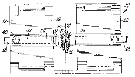
Figures 1-3 illustrate a welder 10 in accordance with this
invention. In general, welder 10 is of the construction of the
welder disclosed in U.S. Patent No. 5,279,685. Welder 10
includes a pair of aligned tube holders 12,12. Each tube holder
includes an upper jaw 14 and a lower jaw 16 movable relative to ~ -~
each other to selectively releasably clamp a plastic tube 18
between each set of upper jaw and lower jaw. The tube holders are
spaced apart to form a gap between the tube holders 12,12. The ;
ends of the tubes 18,18 extend into the gap slightly spaced from
each other. As later described a wafer 20 is moved through the gap
and preferably is heated for melting the ends of the tubes so that `~
the melted tube ends could be pressed into contact with each other ~ ~
to connect the tube ends for forming a single unitary -tube. , ;
Preferably, this is accomplished by a melt/wipe technique as ~
disclosed in the various parent applications. ~-
.: ~
The structure of the tube holders and clamp jaws is
generally similar to that of U.S. Patent No. 5,279,685.
~ 6 ~;
: "':
2118426 :~
~. . - ...... . ~ .
-.,; ~, ,
. .. .
.. . . ..
Figures 6-7 in particular show the details of wafer 20. :.;` ~.
As shown therein wafer 20 is in the form of a flat plate having a ~-
pair of opposite sides 22,22. Wafer 20 also includes a cut-out or
notch 24 for engagement by a pawl in the home position of the wafer j
in the manner described in U.S. Patent No. 5,279,685. Wafer 20 :`...... ``
also includes ~ pair of wings 26 as described in the various parent `
applications.
Wafer 20 is unique in that it also includes a scoop 28 on
each of its sides. Scoop 28 is located generally in line with -
wings 26 which would be at an elevation which is in the general
plane of the clamped tubes 18 where each upper jaw 14 and lower jaw ~`
16 press against the tube ends to flatten the tube ends. Thus,
scoops 28 are in a position to contact the melted tubes.
As best illustrated in Figures 1-2 each holder includes -~
a cam element 30 in the form of a pin located at the upstream ~-
portion of the gap. Cam elements 30,30 are spaced apart a distance
generally equal to the thickness of wafer 20 where its flat sides
do not lnclude the scoops or wings. Cam elements 30,30 thus assure
the proper positioning of wafer 20 as wafer 20 begins to move
" ~
through the gap between the holders 12,12. The scoops 28,28 in `
combination with the cam elements 30,30 are used to control the ~-
plastic volume of the weld. The tube ends are preferably melted by
the wiping action of the wafer and pressed into contact with each
other to form a precise weld connection. The scoops act as debris ~;~
collectors and~make it possible to achieve a means of controlling
the tube exterior flange sides for optimal strength and aesthetics.
, . ..
~ 2118~26
In this manner reliance on rheology of plastic to move excess away
from the weld site is avoided~ Figure 10, for example, illustrates
a ~ube end where excess plastic has been removed by the scoops
28,28.
Figures 1-2 and 8 illustrate a further feature of this
invention wherein each jaw member is of double jaw construction.
As shown therein each jaw member includes a base portion or fixed
jaw 32 which may be channel shaped to accommodate a spring arm 34.
Spring arm 34 functions as a movable jaw. A pressure plate 36 is
also disposed in the channel formed at the upper portion of base
member 32 to press against spring arm 34. As illustrated in Figure
8 an elongated opening 38 extends through the base member 32, the
spring arm 34 and the pressure plate 36. A suitable fastener, such
as a rivet or bolt 40 (Figures 1-2) secures these members together.
As a result, pressure plate 36 maintains spring arm 34 anchored
over about half of its length with the other half hinged at the
èdge 42 of pressure plate 36.
;The formation of a fixed base or jaw member 32 and the
~ . ,
~spring arm 34 thus results in a double jaw clamp jaw which may be i~
: .
considered spring loaded to effectively press against and seal tha ~ ~
- ~ ~
tube~ ends when the first and second clamp jaws 14,16 are moved
relatively toward each other. With this double jaw technique a
reliable strong tube seal 33 results. One pair of fixed jaws
functions to shut off the tubing and preventing the tubing from
slipping. The other pair of~movable jaws form the seal 33 during
the plastic melt process.
2 ~ 2
` .. `; :~,~
In a preferred practice of the invention the double jaw
formation has the following characteristics. The fixed jaw spacing
is 1.6 millimeters, the jaw tooth size is 0.3 millimeters, the
width (flat tube) is 7.3 millimeters, the movable jaw force is 2
lbs., the length of the spring spacer or pressure plate is 16
millimeters.
Very strong seals are made by using wings that are long
enough to create a smooth molten plastic pool inside the tubing.
This is accomplished by locating the tooth 44 of the fixed jaw 32
as close as possible (e.g. 0.25 mm) to the front 46 of the jaw and
by using the movable jaws. Each wing 26 must protrude beyond the
tooth 44 of the fixed jaw and into the open inside the tubing.
The spring loaded double jaws insure tube seal as the
wings 26 are removed. The spring loaded jaws at a 45 angle of end
46 provide guide edges that funnel the wafer 20 into the centered
position. The fixed clamp ~aws 32 clamp down to seal the liquid
area and thus prevent escape of liquid. A final seal width which
in the preferred range is 0.4 - O.6 mm as shown in Figure 12 is
preferable.
Figures 4A-4E illustrate the use of welder 10 in the
connect process. As shown in Figure 4A the wafer 20 begins to
enter the gap between the tube ends. The heated wafer preferably
..~ ".: .
contacts or simply could be near the tube ends to melt the tube -~
ends in the melt/wipe technique described in the various parent ~ ;
applications. As shown in Figure 4A the wings 26 and scoops 28 ~ -
have not yet entered the gap. Although not illustrated in Figures
-.
2118~2~ :
,;- .. .. .
4A-4E the cam elements 30 would assure the proper positioning of
the wafer 20 as it passes through the gap.
Figure 4B illustrates the next sequence in operation
wherein the wings 26 begin to enter the inside of each flattened
tube end.
Figure 4C shows the next sequence where the wings are
moving out of the gap and scoops 28,28 are removing excess plastic
material.
Figure 4D illustrates the next sequence of operation
wherein the wafer is moving out of the gap at which time or
slightly thereafter the holders 12,12 begin to move toward each
other to press the heated ends of the tubes into contact with each
other and thus result in the unitary tube T shown in Figure 4E.
Figure 5A-5E illustrates the same welder 10 used in a
disconnect procedure. As shown therein a single tube T would be
placed across the holders 12,12 spanning the gap between the
holders. The heated wafer 20 would begin to cut through the tube
in a melting operation as shown in Figure 5A.
Figure 5B illustrates the next sequence in operation
wherein the wings 26 enter the cut tube portions.
- Figure 5C illustrates the next sequence in operation
wherein the scoops 28 remove excess plastic material.
, Figure 5D illustrates the next sequence where the wafer
is exiting from the gap. In this sequence the tube holders 12,12
; may be moved toward the wafer to clean the sealed ends by a heating
operation.
. .
, ,~
~1~8426
..~..-
Figure 5E illustrates the two separated tube sectionsresulting from the procedure.
Figure 9 illustrates the use of the invention for
connection or disconnection of a tube section to the tube section
communicating with a receptacle or bag 50. As shown therein a bag
50 would have a tube section 52 permanently connected thereto. The
ar~angement of Figure 9 illustrates an unopen connection 54 of
another tube section terminating in an end seal 56. The end seal
may be, for example, 1.5 mm.
Figure 10 illustrates the flattened end seal 56 is
illustrated in its plan view.
The invention may be used for connecting and/or discon-
necting plastic tube sections to permit the replacement of various
types of receptacles in a system. For exa~ple, U.S. Patent No.
5,141,592 describes various applications which may be utilized for
practicing the present invention. In such procedures,
periodically it would be desired to replace the bag or receptacle
50 with a different bag. For example, the receptacle or bag 50
could be a CAPD bag or a urinary drainage bag and it would be
periodically desirable to replace the used bag with a new bag.
Additionally, the bag or receptacle 50 may also advantageously be
a blood processing receptacle.
The importance of gaining ~ontrol ovèr the distance, or
compression of the molten plastic when making the weld can be
understood by a simple analogy. For example, when joining the ends
211~42 ~
of waxed candles, to make a long candle from short ends, one finds
very quickly that not pushing the ends close enough together makes
a poor joint. There is not enough molten wax available to form a
strong bond. Similarly, if one pushes too hard the molten wax is
pushed out of the joint area to where the butt ends are pushing
against cold wax. This also makes a weak joint. One learns
quickly, there~ore, there is an optimum amount of pushing that
results in an acceptable joint.
In a general way, this analogy carries over to making
strong sterile joints in plastic tubing. Unlike wax candles
sterile connection joints require very reliable consistent highest
strength welds. To achieve these conditions control of the plastic
temperature and compression distance is extremely important. For
example, the inventors have established the data shown in Figure 12
when using medical gray (class 6) PVC tubing 5.4 mm O.D. and 4.0 mm
I.D. while maintaining a wafer temperature of 350C.
As can be seen from Figure 12 the range for acceptable
strength is extremely narrow and therefore the cam control of clamp
distance as provided by the present invention is a novel and
effective means of administering the controls.
Similarly, the use of cams located on the clamped
surfaces can be used to control another vital area of making strong
sterile connectin~s in tubing. When welds are made in tubes that
contain liquid (as illustrated in Figures 2-3) it is necessary to
clamp the tubes in the weld area to avoid liquid escape. During
the welding process a membrane is formed within the tube that must
: ;:
12
211~426
.. .. ..
be broken to reestablish the liquid flow in the lumenO If the
membrane is too thin then liquid flow is not stopped. If the
membrane is too thick the liquid flow can not be reestablished.
Control of the membrane thickness therefore is important. This
control is accomplished by controlling the position of the scoops
28. Figure 11 illustrates the control area B,B with the seal area
A. The seal 58 takes place at portion 56. The scoops 28 under
control of the cams 30 for accurate positioning removes the seal
area A and the scoops are positioned to obtain reproducible and
reliable thickness of the membrane. The invention has the
advantages of maximizing the seal strength by controlling the
compression distance. Additionally, the cams 30,30 engaga the
wafer 20 to control the penetration of the wings 26 during ths
disconnect procedure. The flange height is controlled by remoying
excess material with scoops 28,28. Cams 30,30 insure that the
wafer 20 is properly positioned in a vertical orientation.
Figures 13-15 illustrate a modified form of wafer in
acc,ordance with this invention. The wafer shown therein would be
of'generally the same construction as wafer 20 shown in Figures 6-
7. In Figures 13-15, however, the wafer also includes a slit 50
extending completely through the wafer downstream from scoop 28.
As illustrated slit 50 extends inwardly from the downstream
: ge,nerally vertical trailing edge in a straight line generally
horizontal direction toward the upstream generally vertical leading
edge o~ wafer 20. Slit 50 terminates downstream from scoops 28.
Slit 50 may be of any suitable dimension and preferably has a
.~`.', .
13
. ~ ,.~ ..
~ '''~"~``','
211~42~
.. .. .
length of 7mm and a width of 0.5 mm. Slit So is disposed in line
with scoop 28 and wing 25 on each of the sides 22 of wafer 20.
The advantage of providing a slit, such as slit 50 in the
heated wafer downstream from the scoops 28 is to permit the molten
material from the tubes lB to begin contacting each other at an
earlier time while the tubes are still in the area of the heated
wafer. Figure 15, for example, shows the molten ends of tubes 18
to enter the slit 50 before the wafer 20 has completely cleared
contact with the tubes 18,18. The resultant joint, which is
illustrated in Figure 16, after the tubes have been opened into
communication with each other is of increased strength leaving only
a slight residue 52,52 at the joint.
The invention has the advantages of assured sterility and
maximum weld strength. The invention could be used with a wide
range of plastic material~ such as PVC, polyurethane, hytrel,
nylon, polyethylene, polypropylene and various compositionæ of
Teflon~Y The invention results in improved aesthetics and in the
control of the lumen re-opening requirements.
The present invention also includes features in the wafer
to assure single use of a wafer. Advantageously, the preferred
practice of this invention requires minimal modifications to the
wafer and total containment device.
Figures 17-22 show the details of a single use wafer 120.
As shown therein wafer 120 is in the form of a flat plate having a
pair of opposite sides 122,122. Wafer 120 also includes a cut-out
or notch 124 for engagement by a pawl in the home position of the
14
211~2~
;,.. ` .. ..
wafer in the manner previously described with respect to wafer 120.
Wafer 120 also includes a pair of wings 126.
Wafer 120 also includes a scoop 128 on each of its sides.
Scoop 128 is located generally in line with wings 126 which would
be at an elevation which is in the general plane of the clamped
tubes 118 where each upper jaw and lower jaw press against the tube
ends to flatten the tube ends. See Figure 29 and U.S. Patent No.
5,279,685. Thus, scoops 128 are in a position to contact the
melted tubes.
The wafer 120 also includes a slit 150 extending
completeIy through the wafer downstream from scoops 128. As
illustrated slit lS0 extends inwardly from the downstream generally
vertical trailing edge in a straight line generally horizontal
direction toward the upstream generally vertical leading edge of
wafer 120. Slit 150 terminates downstream from scoops 128. Slit
150 may be of any suitable dimension and preferably has a length of
7mm and a width of 0.5 mm. Slit 150 is disposed in line with scoop
128 and wing 126 on each of the sides 122 of wafer 120.
In order to assure the single use of the wafer, wafer 120
is provided with a hole or aperture 136 at any suitable location
such as being generally in line with notch 124. Aperture 136 is
intended to be covered by a sensing material 138. This can ba
conveniently accomplished by forming the wafer as a plate which is
folded upon itself at one end 140 so that the wafer 120 is of
double thickness, as best shown in Figures 18 and 20-22. Prior to
the complete folding the sensing material 138 is positioned to
-
~ 211 8426
cover hole 136. Material 138 is preferably selected to be of
material which would melt or otherwise be destroyed upon the
heating of the wafer. Thus, once there has been a single use of
the wafer, material 138 no longer covers aperture 136 and can not
be sensed in an attempted second use of the wafer.
Figures 29-30 illustrate, in general, portions of the
total containment device 110 of the type described in U.S. Patent
No. 5,279,685. As shown therein device 110 includes a carriage 112
for moving the wafer through the device. U.S. Patent No. 5,279,6~5
discloses the inclusion of various sensors, such as for indicating
that the wafer is properly loaded in the carriage and for detecting
that the wafer is properly conditioned with respect to the
clenching block. Figure 30 illustrates one such sensor 114 which,
in the device of the parent patent, functions as the aperture
blockage sensor. Sensor 114 is mounted in the path of movement of
aperture 136 and thus would sense aperture 136 passing through the
path of view of sensor 114. Thus, the present invention advanta-
geously makes use of a sensor already in device 110 for its single
use sensing operation. If desired, however, one of the other
sensors or a completely additional sensor may be used for this
purpose.
In operation, as wafer 120 is moved in a downstream
direction sensor 114 views aperture 136. If there is sensing
material 138 located in aperture 136 the material will be sensed.
Such sensing could be in terms, for example, of a voltage reading
which would differ from the voltage reading of the copper wafer
16
~ 211~426
. .............. . .
material 120 and would differ from the voltage reading of a
completely open hole 136. If the sensor 114 does not detect the
proper voltage which would result from the proper sensing material
138 being in aperture 136 then the device 110 would be inactivated.
This would mean that either the wafer 120 had been previously used
and no longer has sensing material 138 or that there is a manufac-
turing defect and the sensing material was not mounted over hole
136.
When the sensing material 138 is properly detected and
other device requirements are met, the wafer 120 is heated for use
in the selective connect/disconnect of the plastic tubes 118,118.
The heating operation results in a melting of sensing material 138
so that hole 136 is completely exposed.
The concept of sensing a condition of the wafer which
would indicate whether or not the wafer has been previously used
can be practiced in various manners. Figure 17A, for example,
illustrates the provision of two holes 136A,136B, each with a
sensing material 138A,138B. Sensing materials 138A and 138B may be
the same or different materials. This arrangement wauld provide a
more sophisticated reading to- require a binary or sequential
voltage reading from sensor 114 in order to prevent device 110 from
being inactivated. Such more sophisticated reading would be
desirable to make it more difficult for a user to attempt to insert
sensing material back into wafer 120 after the wafer has already
been used.
17
211~'~26
.. ..
Cover material 138 is preferably a two mil thick polyeth-
yIene sheet which may contain carbon black. Such material could
also be used as material 138A. Material 138B could llkewise be the
same material or could be a material having a different voltage
characteristic.
Figure 17B shows yet another practice of this invention
wherein the aperture 136C is an elongated slot. The cover material
138C could be the same as cover material 138 or could simply be any
suitable material, preferably a transparent material having some
indicia thereon which would be detected by the sensor. For
example, the indicia could be a bar code or some form of alphanu-
meric code. The indicia could be visible to the naked eye or could
be invisible tQ the naked eye since it is only necessary that the
indicia be visible to the sensor.
Figures 23-28 illustrate wafer 120 mounted in a suitable
holder 160 which could be of the same general construction as the
holder illustrated in Figure 14 of U.S. Patent No. 5,279,685. The
purpose of the holder is to mount wafer in the carriage, during the
initial movement of wafer 120. Holder 116 generally includes a
split body 162 having ia slot 164 into which wafer 120 would be
slidably mounted. Interior of body 162 would include two registra-
tion recesses for receiving lugs 168 on wafer 120. Holder body 162
includes downward extensions 170 which have half round filets 172
to increase the frictional contact on wafer 120 by the spring
action of the body extension 170 which thus act as spring arms.
18
. :.
: .. ..
2118426
In operation, wafer 120 would be mounted in holder 160
during the initial positioning of the wafer in carriage 112. As -~
the wafer is moved downstream it is detached from holder 160 ~
thereby ex~osing slit 150 which is initially covered by extension ;;.
170 of holder 160.
It is to be understood that the holdèr 160 illustrated in `;` .
Figures 23-28 may be used with the type of wafer such as wafer 20
and is not limited to the type of wafer intended for single use `~
purpose. Even where holder 160 is used for a single use wafer, the ~ .
holder itself may be reused multiple times. ~-
,,::... .
. , ,
~ "~ ,, ~,,
: .'~.- `"''
,..i :.
: ' '
19 ~`~