Note: Descriptions are shown in the official language in which they were submitted.
... - 1 2ll~637
Information Recording Method and
Information Recording Apparatus
BACKGROUND OF THE INVENTION
Field of the Invention
The present invention relates to an information
recording method and an information recording
apparatus. Note that the information recording
apparatus of the present invention includes one having
a reproduction function.
Related Background Art
As a recording method for recording bit
information, a magnetic recording method using a
magnetic tape, a magnetic disk, or the like, an
electrical recording method using a semiconductor
element, and the like are known. In recent years,
requirements for a large capacity, a high-speed
operation, and a decrease in error rate have become
strong with an increase in amount of information to be
recorded.
In such a situation, an element which has a
metal-organic insulating film-metal structure in which
an organic thin film (e.g., a thin film of a
~-electron-based organic compound, a ohalcogenide, or
the like) is sandwiched between metal electrodes, and
has a - - y effect with respect to the switching
characteristics of a voltage current (to be referred to
,
37
- 2 -
1 as an ~MIM~ element hereinafter) was developed
(Japanese Laid-Open Patent Application No. 63-096956). -
In such an MIM element, when a proper pulse voltage is
applied across the metal electrodes, the conductivity
of the element can be reversibly changed. Therefore,
by utilizing this switching phenomenon, information can
be recorded in the MIM element. In addition, in this
switching phenomenon, the switching speed is very high.
Fig. 1 is a schematic diagram showing a
conventional recording apparatus utilizing the MIM ~ -
element.
A recording apparatus 2010 includes a recording
medium 2011, a current amplifier 2012, and a recording
voltage generating circuit 2013. The recording medium
2011 includes a lower electrode 20111, an upper
electrode 20112, and a recording layer 20113 which is
arranged between the upper and lower electrodes 20112
and 20111, and consists of an LB film having different
conductivities p between a non-recording state and a
recording state. More specifically, the recording
medium 2011 has the element structure of the
above-mentioned MIM element. The recording voltage
generating circuit 2013 generates a recording voltage
(recording pul~e voltage), and applies the generated
recording voltage across the lower and upper electrodes
20111 and 20112, thereby applying the recording voltage
to the recording layer 20113. The current amplifier
., . , . : , : . :.. : ., i, .. , . i. .. . .
2ll8637
- 3 -
2012 detects and amplifies a current flowing between
the lower and upper electrodes 20111 and 20112 during
application of the recording voltage.
The operation of the recording apparatus 2010 will
be described below. A case will be exemplified wherein
the conductivity p of the recording layer 20113 is -
increased by applying a recording voltage to the
recording layer 20113 which has a small conductivity p
in a non-recording state, and information is thus
recorded. ~ ~
The recording voltage generating circuit 2013 ; -
applies a recording voltage trecording pulse voltage)
of a voltage value V0 to the recording layer 20113 from
time t~ to time t2, as shown in Fig. 2A. At this time,
the conductivity p of the recording layer 20113 changes
from a small conductivity PL to a large conductivity PH
at time t3 (t1 < t3 < t2), as shown in Fig. 2B.
Therefore, the current value increases at time t3 in the
current waveform detected by the current amplifier
2013. In contrast to this, the conductivity p often
does not change within a predeteL ~ ned period of time
or by the predetel ~ ne~ voltage value V0 due to a
variation in element constituting the recording layer
20113. In this case, the current waveform detected by
the current amplifier 2012 has a constant current value
from time t1 to time t2, as shown in Fig. 2C.
2ll8637
- 4 -
In recent years, a scanning tunneling microscope
(STM) which allows observation of a material surface on
the atomic order has been developed, and real space ~
observation at atomic and molecular levels is realized :
(G. Binning et al., Phys. Rev. Lett, 49, 57, 1982). In
the sc~nning tunneling microscope, the distal end (tip)
of a probe electrode is two~ ionally sc~nned while
controlling the distance between the tip and a
conductive sample, so that the value of a tllnnel;ng
current flowing between the tip and the sample bec es
constant, and information of a charge cloud on the
sample surface or the shape of the sample is observed
on the order of sllhn~nr -ters (atomic order) on the
basls of a control signal for controlling the distance
between the tip and the sample at that time.
If the principle of such a scAnning tunneling
microscope is applied, high-density
recording/reproduction can be sufficiently realized on
the atomic order. For example, in a
recording/reproduction apparatus disclosed in Japanese
Laid-Open Patent Appllcation No. 61-80536, information
is recorded by knocking out atomic particles adsorbed
in the surface of a recording medium by, e.g., an
electron beam, and recorded information is reproduced
by the scAnn~ng tunnellng microscope. In a
recording/fep~od~ction apparatus disclosed in USP
No. 4,575,822, an electrical charge is injected into a
_ 5 _ ~ ~863
dielectric formed on the surface of a recording medium
using a tunneling current flowing between the tip and ;~
the surface of the recording medium, thereby recording ~-
information. Furthermore, a method of recording
information by a physical or magnetic decay of a -~
recording medium using a laser beam, electron beam,
particle beam, or the like has also been proposed.
Also, a recording/reproduction method which uses,
as a reoording layer, the above-mentioned thin film
layer consisting of a material having a memory effect
with respect to the switching ph~n ~non of a current
voltage charaateristics, and performs ~ A
,eaoLding/repro~uc1ng by utilizing the principle of the
8C~nn1 n~ tunneling microscope has been proposed
(Japanese Laid-Open Patent Application No. 63-161552 or ~ ~
63-161553). According to this recording/reproduction ~;
method, if the size of a recording bit is 10 nm,
large-c~p~clty recording/reproduction of 1012 bits/cm2
can be realized. For example, a recording/reproduction
apparatus 3000 according to this recording/reproduction
method includes a ~eco.ding medium 3001, a recording
medium stage 3010, a coarse -v. - t ~ch~n1 sm 3011, an
XY direction coarse ~v~ -rt control circuit 3012, a Z
direction coarse movement control aircuit 3013, a probe
electrode 3014, an XY direction fine ;v~ --t ~~h~n1sm
3015, a Z direction ~ine l~v~ Pnt mechanism 3016, an XY
direction fine vl- ?nt control circuit 3017, a Z
~ 6 - ~1~7
direction fine movement control circuit 3018, a current -
amplifier 3019, a microcomputer 3020, a first servo
circuit 3021, a second servo circuit 3022, and a power
source 3023, as shown in Fig. 3. The respective
constituting elements of the recording/reproduction
apparatus 3000 will be described in detail below.
(1) Recording Medium 3001
As shown in Fig. 3, the recording medium 3001 is
constituted by a substrate 3002, a substrate electrode
3003 formed on the substrate 3002, and a recording
layer 3004 formed on the substrate electrode 3003. The
recording layer 3004 comprlses a thin film layer
consistlng of a material having a - ~_y effect with
respect to the switching phen anon of the voltage
current characteristics.
(2) Recording Medium Stage 3010, Coarse Movement
ch~n~sm 3011, XY Direction Coarse Movement
Control Circuit 3012, and Z Direction Coarse
Mo~ t Control Circuit 3013
The recording medium stage 3010 carries the
recording medium 3001 thereon. The coarse ~v~ ~nt
- h~n~ ~ 3011 coarsely moves the recording medium
stage 3010 in the X-, Y-, and Z-axis directions in
Fig. 3, thereby moving the recording medium 3001 in the
X-, Y-, and Z-axis dlrectlons ln Flg. 3. The XY
direction coarse mov~ ont control circuit 3012 is
controlled by the microcomputer 3020, and drives the
.
; , I ,: :
~ ; ~ " ~ ;, ": ,,,,: ~ :-: :
_ 7 _ 21l 8 6~ 7
~:.
coarse mov~ ?nt mechanism 3011 in the X- and Y-axis
directions in Fig. 3. The Z direction coarse movement
control circuit 3013 drives the coarse movement
?chAnism 3011 in the Z-axis direction in Fig. 3 in
accordance with a coarse )v -nt control signal sent
from the first servo circuit 3021.
(3) Probe Electrode 3014, XY Direction Fine ~ov.~ -nt
~P~hAni1 3015, Z direction Fine ~av~- ?nt - -~
MechAn1! 3016, XY direction Fine ~lov -- t Control
Circuit 3017, and Z direction Fine S~v~ -nt
Control Circuit 3018
The probe electrode 3014 is positioned above the
surface of the recording medium 3001. The XY direction
fine -,~ t ochAnism 3015 finely moves the probe
electrode 3014 in the X- and Y-axis directions in Fig. 3,
thereby two-dimensionally scAnning the probe electrode
3014 with respect to the recording medium 3001. The Z
direction fine -~ t schAnlsm 3016 finely moves the
probe electrode 3014 in the Z-axis direction in Fig. 3,
thereby finely adJusting the distance between the probe
electrode 3014 and the recording medium 3001. The XY
direction fine v -nt control circuit 3017 is ~ ;
aor.~lolled by the microcomputer 3020, and drives the XY
dlrectlon flne movement mech~nism 3015 ln the X- and
Y-axis dlrectlons in Flg. 3. The Z direction flne
~ nt control circuit 3018 drives the Z direction
fine movement ?chAnism 3016 in the Z-axis direction in
8 - 211 8 6
1 Fig. 3 in accordance with a fine movement control
signal sent from the second servo circuit 3022.
(4) Current Amplifier 3019, Microcomputer 3020, First
Servo Circuit 3021, Second Servo Circuit 3022, and
Power Source 3023
The current amplifier 3019 detects and amplifies a
current flowing between the probe electrode 3014 and
the recording medium 3001, and outputs the amplified
current to the microcomputer 3020, and the first and
second servo circuits 3021 and 3022. The first servo
circuit 3021 compares the value of the current sent
from the current amplifier 3019 with a first current
setting value, supplied from the microcomputer 3020,
for maint~lning a predetermined distance between the
probe electrode 2014 and the recording layer 3004, and
outputs a coarse movement control signal for performing
coarse ,v. --t control of the distance between the
probe electrode 3014 and the recording medium 3001 to ;~.
the Z direction coarse movement control circuit 3013.
rrhe second servo circuit 3022 compares the value of the
current sent from th~ current amplifier 3019 with a
second current setting value, supplied from the -~
microcomputer 3020, for maint~ining the predetermined
distance between the probe electrode 2014 and the
recording layer 3004, and outputs a fine movement
control signal for'performing fine movement control of
the distance between the probe electrode 3014 and the
......
; , . , , , ' ,' ' ' ': '
~ ~, , ; , . . - ..
9 ~$~7
1 recording medium 3001 to the Z direction fine -v.- ~t
control circuit 3018. The power source 3023 applies,
between the recording medium 3001 and the probe
electrode 3014, a recording bias voltage and a
recording pulse voltage in a recording mode, a
reproduction bias voltage in a reproduction mode, and
an erasing bias voltage and an erasing pulse voltage in
an erasing mode. The microcomputer 3020 controls the
XY direction coarse mov~ -nt control circuit 3012, the
XY direction fine -,v~ -nt control circuit 3017, and
the power source 3023, and outputs the above-mentioned
first and second current setting values to the first
and second servo circuits 3021 and 3022, respectively.
The recording and reproduction operations of the
recording/reproduction apparatus 3000 will be described
below.
In the recording mode, the power source 3023 is
controlled by the microcomputer 3020 to apply a
predetermined bias voltage to the substrate electrode
3003 of the recording medium 3001. Thus, the
predetermined bias voltage is applied between the probe ~
electrode 3014 and the recording layer 3004 of the
recording medium 3001. At this time, a current flowing
between the probe electrode 3014 and the recording
layer 3004 is detected and amplified by the current
amplifier 3019, and the amplified current is sent to
: .
: ; ,,
lo ~ 637
1 the microcomputer 3020l and the first and second servo
circuits 3021 and 3022.
The first servo circuit 3021 compares the value of
the current sent from the current amplifier 3019 with
the first current setting value sent from the
microcomputer 3020, and outputs, to the Z direction
coarse movement control circuit 3013, a coarse movement
control signal for performing coarse movement control
of the distance between the probe electrode 3014 and
the recording layer 3004, so that the two values become
equal to each other. The Z direction coarse .v~ -nt
control circuit 3013 generates a signal for driving the
coarse movement mechanism 3011 in the Z-axis direction
in Fig. 3 on the basis of the coarse movement control
signal, and outputs the generated signal to the coarse
movement mechanism 3011. With this signal, the
distance between the probe electrode 3014 and the
recording layer 3004 is coarsely ad~usted. The second
servo circuit 3022 compares the value of the current
sent from the current amplifier 3019 with the second
current setting value sent from the microcomputer 3020,
and outputs, to the Z direction fine movement control
circuit 3018, a fine movement control signal for
performing fine movement control of the distance
bet~.een the probe electrode 3014 and the recording
layer 3004, 80 that the two values become equal to each
other. The Z direction fine mov - t control circuit
. . .
.... :. .
,
."
. .
2~ 3 7
1 3018 generates a signal for driving the Z direction
fine mov~ -nt mechanism 3016 in the Z-axis direction in
Fig. 3 on the basis of the fine mov -nt control
signal, and outputs the generated signal to the Z
direction fine moveme~t mechanism 3016. With this
signal, the distance between the probe electrode 3014
and the recording layer 3004 is finely adjusted, i.e.,
the predetermined distance is maintained.
The XY direction coarse movement control circuit
3012 generates a signal for driving the coarse movement
mechanism 3011 in the X- and Y-axis directions in
Fig. 3 on the basis of an instruction from the
microcomputer 3020, and outputs the generated signal to
the coarse movement mechanism 3011. The XY direction
fine mov~ t control circuit 3017 generates a signal
for driving the XY direction fine movement mechanism
3015 in the X- and Y-axis directions in Fig. 3 on the ~ n
basis of an instruction from the microcomputer 3020,
and outputs the generated signal to the XY direction
fine movement mechanism 3015. Thus, the probe
electrode 3014 is scAnned to the recording position of ;-
the recording medium 3001. ~
The power source 3023 generates a recording bias ~ ~'
voltage and a recording pulse voltage on the basis of
an instruction from the microcomputer 3020. The
recording bias voltage and the recording pulse voltage
are applied to the recording layer 3004 via the
- 12 _ 21 1 863 7
1 substrate electrode 3002 of the recording medium 3001.
With these voltages, since the conductivity of a
portion, applied with the recording pulse voltage, of
the recording layer 3004 locally changes, a recording
bit is formed on the recording layer 3004.
In the reproduction mode, the probe electrode is
scanned to the reproduction position of the recording
medium 3001 in the same manner as in the recording
mode. Thereafter, the power source 3023 generates a
reproduction bias voltage. The reproduction bias
voltage is applied to the recording layer 3004 via the
substrate electrode 3002 of the recording medium 3001.
At this time, a current flowing between the probe
electrode 3014 and the recording layer 3004 is detected
and amplified by the current amplifier 3019, and the
amplified current is sent to the microcomputer 3020.
The microcomputer 3020 calculates the conductivity of
the recording layer 3004 on the basis of the value of
the sent current. Since the presence/absence of a
recording blt can be detected based on the value of the
calculated conductivity, recorded information can be
reproduced.
In the above-mentioned conventional
recording/reproduction apparatus 3000, when the
recording medium 3001 is replaced by a crystal such a~
silicon, atomic-level recording and processing can be
performed. More specifically, the probe electrode 3014
, ' ~
I
,: . . - - . : . .
- 13 - 2~1 $ 63 7
is moved to a recording position where information is
to be recorded, and a voltage is applied at the
recording position to move one of atoms on the surface
of the recording medium 3001 as a recording bit.
However, the conventional recording apparatus 2010
shown in Fig. 1 suffers from the following problems.
(1) When the predetermined voltage value V0 and
the recording pulse voltage of the predete, ;nP~ pulse
width (tz - t1) are applied to the recording layer
20113, information can be accurately recorded in some
cases, but cannot be accurately recorded in some other
cases, resulting in a large recording error rate.
(2) If the pulse width (t2 - tl) of the recording '~
pulse voltage is increased to assure stable information
recording, the operation speed is lowered.
(3) Even when information is accurately recorded,
since an excessive current flows during a time interval
from time t3 to time t2, as shown in Fig. 2B, the
elements constituting the recording layer 20113 may be
deYtLuyed.
The corl-ventional recording/reproduction apparatus
3000 shown in Fig. 3 also suffers from the same
problems as those of the conventional recording
apparatus 2010 shown in Fig. 1.
Furthermore, in a recording apparatus using a
scanning tllnneling microscope, a recording error may be
caused by nonllniformity of a recording medium in the
I
, .
,, , , " , . . .
~ - 14 - ~11863~
recording mode. In the conventional recording
apparatus 2010 shown in Fig. 1, a voltage necessary for
changing the conductivity may vary due to variation of
characteristics between individual device. When a
voltage higher than a required voltage is applied, the
LB film may be destroyed.
In a surface atom processing technique or a
recording technique using it, a voltage required for
processing an atom at or near a defect position is
different from an atom present on a normal terrace. If
the voltage is too low, atom processing may often be
disturbed; if the voltage is too high, the high voltage
may also influence llnnecess~ry atoms.
The problem of a recording error caused by
nonlln~formity flep~n~ng on recording positions is posed
not only when a voltage is applied but also in the
surface processing techniques or the recording
techniques using the sc~nn ~ ng tunnel electrode, e.g.,
when mechanical processing is performed by br~ ng~ ng the
probe into contact with the surface of the recording
medium or sample.
This problem is also posed when a recording bit is
formed or fine processing is performed using not only
the scanning tunnel electrode but also various types of
8C~nn~ ng probe microscope (SPM) such as an interatomic
force microscope (AFM).
. ~
- ,
- 15 -
~ 211~3 7
1 SUMMARY OF THE lNVh~lION
It is an object of the present invention to
provide an information recording method and an
information recording apparatus, which can reliably
record information without damaging elements
constituting a recording layer.
It is another object of the present invention to
provide a recording apparatus, a recording/reproduction
apparatus, a recording method, and a ...
recording/reproduction method, which can reliably
record information on a recording medium, and can
pLevent destruction of a recording medium.
It is still another ob~ect of the present
invention to provide an information recording apparatus ~::
and an information recording method, which can reliably
process the surface of a material using a sc~nning
probe microscope, and can plevent unnecessary
processing.
In order to achieve the above objects, there is
provided an information recording method for recording
information by locally applying a physical action to a
recording medium in accordance with information,
comprising the steps of: locally applying the physical
action to the recording medium in accordance with
information; measuring a physical quantity of a
portion, applied with the physical action, of the
recording medium; and confirming recording of the
;; . ' .; .,,, !, ,
' ' ~.
' . ' ' :' " ' " ' '.':
- 16 ~ 637
information on the basis of the measured physical
quantity.
There is also provided an information recording
apparatus for recording information by locally applying
a physical action to a recording medium in accordance
with information, comprising: means for locally
applying the physical action to the recording medium in
accordance with information; means for measuring a ~;
physical quantity of a portion, applied with the
physical action, of the recording medium; and means for ~- -
confirming recording of the information on the basis of
the measured physical quantity.
Note that the physical action in the present
invention includes a current, voltage, force, magnetic
force, light, and the like, and the physical quantity
includes a current, voltage, force, magnetic force,
light, and the like, and their differential values,
integral valuesf and the like.
BRIEF DF~CRIPTION OF THE DRAWINGS
Fig. 1 is a sche -tic diagram showing a prior art
of a recording apparatus using an MIM element;
Figs. 2A to 2C are graphs for expl~ln~ng the
operation of the recording apparatus shown in Fig. 1,
in which Fig. 2A is a graph showing the waveform of a
recording voltage, Fig. 2~ is a graph showing the
waveform of a current detected and amplified by a
- 17 _ ~ 6~ 7
current amplifier obtained when the conductivity of a
recording medium shown in Fig. 1 changes, and Fig. 2C
is a graph showing the waveform of a current detected
and amplified by the current amplifier obtained when
the conductivity of the recording medium shown in
Fig. 1 does not change;
Fig. 3 is a schematic diagram showing a prior art
of a recording/reproduction apparatus; ~-
Fig. 4 is a schematic diagram showing the first
embodiment of a recording apparatus according to the
present invention; ~ -
Figs. 5A to 5C are equivalent circuit diagrams of
a recording medium shown in Fig. 4, in which Fig. 5A
shows a general equivalent circuit of the recording
medium, Fig. 5B shows an app~oximate equivalent circuit
obtained when the conductivity of the recording medium
is small, and Fig. 5C shows an approximate equivalent
circuit obtained when the conductivity of the recording
medium is large;
Figs. 6A to 6C are graphs showing the waveforms of
a current to be detected by a current amplifier shown
in Fig. 4, Fig. 6A is a graph showing the waveform of a
recording pulse voltage, Fig. 6B is a graph showing the
waveform of a current deteated by the current amplifier
when the conduativity of the recording medium
increases, and Fig. 6C is a graph showing the waveform
.,
', ' ' ' ' ~ ;, ' . ' '.'" ~, , '
' - 18 - ~ 3l7
1 of a current detected by the current amplifier when the
conductivity of the recording medium does not change;
Figs. 7A and 7B are schematic views showing the
second embodiment of a recording apparatus according to
the present invention, in which Fig. 7A is a schematic ~ -
diagram of the recording apparatus, and Fig. 7B is a ;
side view of a recording medium;
Fig. 8 is a schematic diagram showing the third
embodiment of a recording/reproduction apparatus
according to the present invention;
Fig. 9 is a schematic diagram showing the fourth
embodiment of a recording apparatus according to the
present invention;
Figs. lOA and lOB are graphs for expl~jning the
operation of the recording apparatus shown in Fig. 9,
in which Fig. lOA is a graph showing the waveform of a
recording voltage, and Fig. lOB is a graph showing the
waveform of a current detected and amplified by a
current amplifier shown in Fig. 9;
Figs. llA and llB are schematic views showing the
fifth embodiment of a recording apparatus according to
the present invention, in which Fig. llA is a schematic
diagram of the recording apparatus, and Fig. llB is a
left ~ide view of a recording medium;
Fig. 12 is a schematic diagram showing the sixth
embodiment of a recording/reproduction apparatus
according to the present invention;
, . . : ~
. ~ - 19 _ 2llg637
1 Figs. 13A and 13B are graphs for explaining the
operation of the seventh embodiment of a
recording/reproduction apparatus according to the
present invention, in which Fig. 13A is a graph showing
the waveform of a recording voltage, and Fig. 13B is a
graph showing the waveform of a current detected and
amplified by a current amplifier shown in Fig. 12; ~ ~;
Fig. 14 is a schematic diagram showing the eighth
embodiment of a recording apparatus according to the
present invention;
Figs. 15A and 15B are graphs for explaining the
operation of the recording apparatus shown in Fig. 14,
in which Fig. 15A is a graph showing the waveform of a
recording current, and Fig. 15B is a graph showing the
waveform of a voltage detected and amplified by a
voltage amplifier shown in Fig. 14;
Fig. 16 is a schematic diagram showing the 11th
embodiment of a recording/reproduction apparatus
according to the present invention;
Figs. 17A and 17B are graphisi for expli~ining an
example of the operation of the recording/reproduction
apparatus shown in Fig. 16, in which Fig. 17A i8 a
graph showing the value of a voltage to be applied to a
recording medium in a recording mode, and Fig. 17B is a
graph showing the value of a current amplified by a
current amplifier;
.
~:i~ . ' ' ' ' ' , , . . '' . ~' ' ".:' '
- 20 _ ~11 8 63'~
1 Figs. 18A and 18B are graphs for explaining
another example of the operation of the
recording/reproduction apparatus shown in Fig. 16, in
which Fig. 18A is a graph showing the value of a
voltage to be applied to the recording medium in the
recording mode, and Fig. 18B is a graph showing the
value of a current amplified by the current amplifier;
Figs. l9A and l9B are graphs for explaining still
another example of the operation of the
recording/reproduction apparatus shown in Fig. 16, in
which Fig. l9A is a graph showing the value of a
voltage to be applied to the recording medium in the
recording mode, and Fig. l9B is a graph showing the
value of a current amplified by the current amplifier;
Figs. 20A and 20B are graphs for expl~ining still
another example of the operation of the
recording/reproduction apparatus shown in Fig. 16, in
which Fig. 20A is a graph showing the value of a
voltage to be applied to the recording medium in the
recording mode, and Fig. 20B is a graph showing the
value of a current amplified by the current amplifier;
Figs. 21A to 21E are graphs for explaining the
operation of the 12th embodiment of a
recording/reproduction apparatus according to the
pre~ent invention, in which Fig. 21A i8 a graph showing
the value of a voltage to be applied to a recording
medium in a recording mode, Fig. 21B is a graph showing ~
, ::
,
~ - 21 _ 21~ ~ 63 ~
,,
an example of the value of a current amplified by a
current amplifier, Fig. 21C is a graph showing another
example of the value of a current amplified by a
current amplifier, Fig. 21D is a graph showing the
differential value of the current shown in Fig. 21B,
and Fig. 21E is a graph showing the differential value
of the current shown in Fig. 21C;
Fig. 22 is a schematic diagram showing the 13th
embodiment of the recording/reproduction apparatus
according to the present invention; ~ -
Figs. 23A to 23F are views for expl~ining the
operation of the recording/reproduction apparatus shown
in Fig. 22, in which Fig. 23A is a graph showing the
result of an experiment for obt~;n;ng the relationship
between the position, in the Z-axis direction in
Fig. 22, of a recording medium driving mechanism, and
the deflection amount detected by a deflection amount
detector, and Figs. 23~ to 23F are views showing
interpretations of a force curve shown in Fig. 23A; and
Figs. 24A and 24~ are graphs for expl~n~ng the
operation of the recording/reproduction apparatus shown
in Fig. 22, in which Fig. 24A is a graph showing a
change, over time, in deflection amount detected by the
deflection amount detector, and Fig. 24B is a graph
showing a change, over time, in position, in the Z-axis
direction in Fig. 22, of the recordlng medium drlving
?-h~n;-
~ . "
~ 22 - ~ ~$~7
1 DETAILED DESCRIP'rION OF THE PREFERRED EMBODIMENTS
The preferred embodiments of the present invention
will be described hereinafter with reference to the
accompanying drawings.
[First Embodiment]
Fig. 4 is a schematic diagram showing the first
embodiment of a recording apparatus according to the
present invention.
A recording apparatus 10 includes a recording
medium 11, a current amplifier 12, a judging circuit
13, and a recording pulse voltage generating circuit
14. The recording medium 11 includes a lower electrode
11l, an upper electrode 112, and a recording layer 113
which is formed between the upper and lower electrodes
112 and 111, and whose conductivity changes upon
application of a voltage. More specifically, the
recording medium 11 has the element structure of the
above-mentioned MIM element. The recording pulse
voltage generating circuit 14 generates a recording
pulse voltage, and applies the generated recording
pulse voltage across the lower and upper electrodes 111
and 112. The current amplifier 12 detects and amplifies
a current flowing between the lower and upper
electrodes 111 and 112 at the time of application of the
LacGLding voltage and after application of the
recording voltage. The ~udging circuit 13 ~udges based
on the value of a current sent from the current
,., ~ ,
". ~; "
~ ~ - 23 - ~ 3! ~ ~
1 amplifier 12 whether or not information is accurately
recorded. If the judging circuit 13 judges that
information is not accurately recorded, it supplies an
instruction to the recording pulse voltage generating
circuit 14 so as to apply the recording pulse voltage
across the lower and upper electrodes 111 and 112 again.
The equivalent circuit of the recording medium 11
when viewed from the recording pulse voltage generating
circuit 14 is expressed by a parallel circuit of an
element resistor R and a capacitor C, as shown in
Fig. 5A. Note that the capacitor C includes the
capacitance of a connection cable, and the like. The ~;
resistance of the element resistor R corresponds to the
reciprocal number of a conductivity p of the recording
medium 11. Therefore, when the conductivity p of the
recording medium is small (p = PL)~ since the capacitor
C becomes dominant, the equivalent circuit of the
.aco ding medium 11 is approximately expressed by only
the capacitor C, as shown in Fig. 5B. When the
conductivity p of the recording medium is large (p =
p~), since the element resistor R becomes dominant, the
equivalent circuit of the recording medium 11 is ~
approximately expressed by only the element resistor R, ~ '
as shown in Fig. 5C.
A case will be examined below wherein information
is recorded by increasing the conductivity p of the
recording medium 11 by applying a recording pulse
,~
. i, . . ~ , . . ... ..
- 24 - 211 8637
. ~ .
l voltage to the recording medium 11 in a state with a
small conductivity p. As shown in Fig. 6A, by applying
the recording pulse voltage to the recording medium 11
from time t~ to time t2, the conductivity p of the
recording medium ll ehanges from a small conductivity PL
to a large conduetivity p~. At this time, the
equivalent circuit of the recording medium 11 is
approximately expressed by only the capacitor C, as
shown in Fig. 5B. Therefore, in the waveform of a
current detected by the current amplifier 12, a current
for charging the capacitor C instantaneously flows at
time t~, and thereafter, exponentially decreases, as
shown in Fiq. 6B.
~hereafter, sinee the eonductivity p of the
lS reeording medium 11 ehanges from the small eonduetivity
PL to the large eonduetivity PH before time t2, the
eleetrieal eharge aeeumulated on the eapaeitor C is
diseharged via the reeording layer 113 of the reeording
medium 11, and at the same, a eurrent flows. In
eontrast to this, when the eonduetivity p of the
reeording medium 11 is left unehanged from the small ~ ;
eonduetivity PL upon applieation of the reeording pulse
voltage, the equivalent eireuit of the reeording medium
11 remains to be expressed approxlmately by only the
eapaeltor C, as shown ln Fig. 5B. Therefore, in the
waveform of a eurrent deteeted by the eurrent amplifier
12 at that time, a diseharge eurrent generated when the
j: i ; ' . ~ ~ ' . .. . ' . . ' j .. , ! ~. . ...
,. i ' ' '
- 25 _ 21~ 86'~ ~
1 electrical charge accumulated on the capacitor C flows
from the lower and upper electrodes 11l and 112 into the
current amplifier 12 instantaneously flows at time t2 at
which application of the recording pulse voltage is
stopped, and thereafter, the current exponentially
decreases, as shown in Fig. 6C. Therefore/ whether or
not the conductivity p of the recording medium changes,
i.e., whether or not information is accurately recorded
can be judged based on the presencetabsence of this
discharge current.
Thus, in the judging circuit 13, as shown in
Figs. 6B and 6C, a reference current value Io is set in
a direction to generate the discharge current. When a
current exceeding the reference current value Io is
supplied from the current amplifier 12 after
application of the recording pulse voltage, it is
judged that information is not accurately recorded. In
this case, the judging circuit 13 outputs, to the
recording pulse voltage generating circuit 14, an
instruction for applying the recording pulse voltage to
the recording medium 11 again. Note that the reference
current value Io can be set to be a value capable of
suppressing an erroneous operation.
Next, a case will be e~rined below wherein
information is recorded by decreasing the conductivity
p of the recording medium 11 by applying a recording
pulse voltage to the recording medium 11 in a state
:, , . :
: .~. . . .
,: ,
:
"" ; ~' '::~'
"~
- 26 _ 21 ~ 863 ~
with a large conductivity p~. When the conductivity p
changes from a large conductivity PH to a small
conductivity PL upon application of the recording pulse
voltage, since the relative c~p~citance of the
capacitor C in the equivalent circuit of the recording
medium 11 increases, the effect of the capacitor C
becc ?S conspicuous. Therefore, i ~iately after the
recording pulse voltage is applied (at the time of
application of the recording pulse voltage), the
current amplifier 12 detects a discharge current of the
electrical charge accu 1l Ated on the capacitor C. In
aontrast to this, when the conductivity p of the
recording medium 11 does not change upon application of
the recording pulse voltage, the effect of the
capacitor C does not appear, and the current amplifier ;~
12 does not detect any discharge current at the time of
application of the recording pulse voltage. Therefore,
in the Judging circuit 13, the reference current value ~
Io ls set in the direction to generate the discharge ~ ;
current. When a current PYGee~ ng the reference
,:
current value Io is not supplied from the current
ampli~ier 12 at the time of application of the
recording pulse voltage, the ~udging circuit 13 Judges
that information is not accurately recorded, thus
de~e- ~ n~ ng whether or not information can be
accurately recorded. When the judging circuit 13
judges that information is not accurately recorded, the ~:
- ~ - ' .: . .. : :,, :
': ' .
I ' , ' ' ,. ' .. ,.. : ~'
- 27 - ~8~
l judging circuit 13 outputs, to the recording pulse
voltage generating circuit 14, an instruction for
applying the recording pulse voltage to the recording
medium ll again.
As described above, in the recording apparatus lO -~
of this embodiment, since application of a recording
voltage to the recording medium 11 can be automatically
repeated until information is accurately recorded, the
error rate in the recording mode can be greatly ;
decreased.
The first embodiment of a recording/reproduction
apparatus according to the present invention will be
described below.
The recording apparatus 10 shown in Fig. 4 has
only a recording function. A recording/reproduction .
apparatus also having a reproduction function can be
realized by Ad~ng, to the apparatus 10, a means for :~
applying a ~epLoduction voltage (reproduction bias :~
voltage) across the lower and upper electrodes 111 and
112 of the recording medium 11 in a reproduction mode, -
and an information reproduction meanR for reproducing
information from a current sent from the current
amplifier 12.
[Second Embodiment~
The second embodiment of a recording apparatus
according to the present invention will be described
below with reference to Figs. 7A and 7B.
,. :, .
.
2118637
- 28 -
1 A recording apparatus 50 includes a recording
medium 51, a recording pulse voltage generating circuit
52, a lower electrode selecting circuit 53, an upper
electrode selecting circuit 54, a current amplifier 55,
a judging circuit 56, and a microcomputer 57. The
respective constituting elements of the recording
apparatus 50 will be described below.
(l) Recording Medium 51
The recording medium 51 includes a lower electrode
group (lower electrodes 51ll to 5118 which are formed to
be parallel to each other), an upper electrode group
(upper electrodes 512~ to 5128 which are formed to be
parallel to each other, and to be perpendicular to the
lower electrode group), and a recording layer 513
consisting of an LB film which is formed between the
upper and lower electrode groups, and whose ~.
conductivity locally changes upon application of a
voltage.
(2) Recording Pulse Voltage Generating Circuit 52,
Lower Electrode Selecting Circuit 53, and Upper
Electrode Selecting Circuit 54
The recording pulse voltage generating circuit 52
generates a recording bias voltage in accordance with
an instruction sent from the microcomputer 57, and also
generates a recording pulse voltage in accordance with
an in8truction sent from the judging circuit 56. The
lower electrode selecting circuit 53 selects one of the
. . :.
,.' ; ~
- 29 - 2~ 8~3'~
1 lower electrode group (lower electrodes 511~ to 5118),
and connects the selected electrode to the recording
pulse voltage generating circuit 52. The upper
electrode selecting circuit 54 selects one of the upper
electrode group (upper electrodes 5121 to 5128), and
connects the selected electrode to the current
amplifier 55.
(3) Current Amplifier 55
The current amplifier 55 detects and amplifies a
current flowing between the lower electrode selected by
the lower electrode selecting circuit 53 and the upper
electrode selected by the upper electrode selecting
circuit 54 at the time of application of a recording
pulse voltage, and after application of a recording
pulse voltage.
(4) Judging Circuit 56
The ~udging circuit 56 judges based on the value
of a current sent from the current amplifier 55 whether
or not information is accurately recorded. If the
~udging circuit 56 determines that information is not
accurately recorded, it supplies an instruction to the
recording pulse voltage generating circuit 52 to
generate a recording pulse voltage again.
(5) Microcomputer 57
The microcomputer 57 controls the recording pulse
voltage generating circuit 52, the lower electrode
:.:
; . :, ~ :. .. : ... . .
-- 30 -
,.. ~ 2118637
selecting circuit 53, and the upper electrode selecting
circuit 54.
The operation of the recording apparatus 50 will
be described below.
When the microcomputer 57 outputs an instruction
for generating a recording pulse voltage to the
recording pulse voltage genera~ing circuit 52, a
recording pulse voltage is generated by the recording
pulse voltage generating circuit 52. The microcomputer
57 outputs an instruction for selecting a lower
electrode to which the recording pulse voltage is to be
applied (e.g., the lower electrode 51l1 at the left end
in Fig. 7A) to the lower electrode selecting circuit
53, and also outputs an instruction for selecting an
upper electrode corresponding to an information ;
recording position (e.g., the upper electrode 512l at
the upper end in Fig. 7A) to the upper electrode
selecting circuit 54. Thus, the recording pulse
voltage is applied between the lower electrode 51
selected by the lower electrode selecting circuit 53,
and the upper electrode 512l selected by the upper
electrode selecting circuit 54, thereby recording
information on the recording layer 513.
A current flowing between the lower electrode 51
selected by the lower electrode selecting circuit 53,
and ~he upper electrode 512l selected by the upper
electrode selecting circuit 54 is detected and
;.~. ' '' ~ ' ~- '
.. . . .
' . ~ . '
~ - 31 _ 21 1 ~ 6 ~ r~
1 amplified by the current amplifier 55. Thereafter, the
amplified current is sent to the judging circuit 56.
The judging circuit 56 judges, using the current sent
from the current amplifier 55, whether or not
information is accurately recorded, by the same method
as in the judging circuit 13 shown in Fig. 4. If it is
dete_ ine~ that information is accurately recorded,
information indicating that information is accurately
recorded is sent from the judging circuit 56 to the
microcomputer 57. Upon reception of this information
from the ~udging circuit 56, the microcomputer 57
outputs an instruction for selecting a lower electrode
to which the recording pulse voltage is to be applied
(e.g., the second lower electrode 51l2 from the left end
in Fig. 7A) to the lower electrode selecting circuit
53, and also outputs an instruction for selecting an
upper electrode correspon~ing to an information
Lecolding position (e.g., the upper electrode 5121 at
the upper end in Fig. 7A) to the upper electrode
~electing circuit 54, so as to select the next
Leco~ding position. On the other hand, if it is
determined that information is not accurately recorded,
information indicating that information is to be
lacorded again is o~LpuL from the ~udging circuit 56 to
the microcomputer 57. Upon reception of this
information from the ~udging circuit 56, the
microcomputer 57 stops the operation for selecting the
, , . . ..... ... - . ,,;, .:,, . : , .:
'~ - 32 _ 11 8 63 ~
1 next recording position. An instruction for generating
a recording pulse voltage again is output from the
judging circuit 56 to the recording pulse voltage
generating circuit 52. Thus, information is recorded
again at the same position on the recording layer 513.
Upon repetition of the above-mentioned operation,
information is two-dimensionally recorded on the
recording medium 51. '
Therefore, in the recording apparatus 50, since a
recording pulse voltage is repetitively applied until
information is accurately recorded, the error rate upon
formation of a recording bit can be greatly decreased. ~'
A~ for the erasing operation in the recording apparatus
50, information recorded on the recording medium 51 can .;
be stably erased by performing the same operation as
the above-mentioned recording operation.
The second embodiment of a recording/reproduction
apparatus according to the present invention will be ~
described below. ~ A
The recording apparatus 50 shown in Figs. 7A and
7B has only a recording function. However, by ~ing
the following functions to the recording pulse voltage
generating circuit 52 and the microcomputer 57, a
recording/~epleductlon apparatus al~o having a
Le~Loduction function can be realized.
,.. : .. ,.,. ,, , , : ,. .:, , ,: .", . . ~ .. ~ .:
- 33 211 ~63 ~
l (1) A function for generating a reproduction
voltage in a reproduction mode is added to the
recording pulse voltage generating circuit 52.
(2) A function for outputting an instruction for
selecting a lower electrode, to which a reproduction
voltage is to be applied, to the lower electrode
selecting circuit 53, and outputting an instruction for ~:~
selecting an upper electrode corresponding to an .
information reproduction position to the upper -
electrode selecting circuit 54 in the reproduction
mode, and a function for reproducing information based
on a current sent from the current ampli~ier 55 in the
~epLoduction mode are added to the microcomputer 57.
In place of adding the function for generating a
~epLoduction voltage in the Leploduction mode to the
recording pulse voltage generating circuit 52 described
in (1) above, means for generating a lep.oduction
voltage in the ~eploduction mode may be separately
arranged.
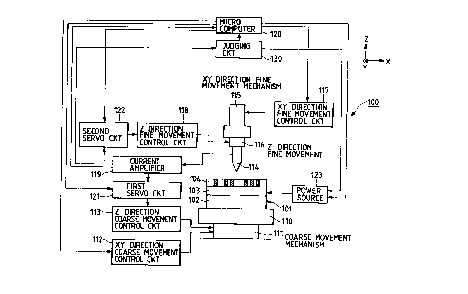
~Third Embodiment]
The third embodiment of a recording/reproduction
apparatus according to the pre~ent invention will be
described below with reference to Fig. 8.
A difference between a recording/reproduction
apparatu8 100 and the conventional
recording/reproduction apparatus 3000 shown in Fig. 3
is that the apparatus 100 comprises a ~udging circuit
- 34 2118637
1 130 for judging based on the value of a current
detected by a current amplifier 119 whether or not
information is accurately recorded, and for, when it is
determined that information is not accurately recorded, :~
supplying an instruction for applying a recording
voltage again be~ en a recording medium 101 and a
probe electrode 114 to a power source 123.
The recording and reproduction operations of the
recording/lep~oduction apparatus 100 will be described
below. .
In a recording mode, the power source 123 applies
a predetermined bias voltage to a substrate electrode
103 of the recording medium 101 under the control of a
microcomputer 120. Thus, the predetermined bias
voltage is applied bet~_cn the probe electrode 114 and
a recording layer 104 of the recording medium 101. A
current detected by the probe electrode 114 at that
time (i.e., a current flowing between the probe
electrode 114 and the recording layer 104) i8 amplified
by the current amplifier 119, and the amplified current
i8 supplied to the microcomputer 120, a first servo
circuit 121, and a second servo circuit 122.
The first ~ervo circuit 121 compares the value of
the current ~upplied from the current amplifier 119
with a first current setting value sent from the
microcomputer 120, and outputs a coarse movement
control signal for performing coarse mov~~ ~1lt control
,, : ...... , , .--,- , , ,.",., - . .. . .
: - 35 - ~1~8637
1 of the distance between the probe electrode 114 and the
recording layer 104, so that the two values become
equal to each other, to a Z direction coarse -,v~ --t -
control circuit 113. The Z direction coarse movement
S control circuit 113 generates a signal for driving a
coarse movement mechanism 111 in the Z-axis direction
in Fig. 8 on the basis of the coarse movement control
signal, and ou~p~s the generated signal to the coarse
movement mechanism 111. Thus, the distance beL~_en the
probe electrode 114 and the recording layer 104 is
coarsely ad~usted. The second servo circuit 122
compares the value of the current supplied from the
current amplifier 119 with a ~econd current setting
value sent from the microcomputer 120, and outputs a
fine movement control signal for performing fine
movement control of the distance bet~een the probe
electrode 114 and the recording layer 104, so that the
two values become equal to each other, to a Z direction
fine movement control circuit 118. The Z direction
fine movement control circuit 118 generates a signal
for driving a Z direction fine movement mech~nism 116
in the Z-axis direction in Fig. 8 on the basis of the
fine movement control signal, and outputs the generated
signal to the Z direction fine movement mechanism 116.
Thus, the distance between the probe electrode 114 and
the recording layer 104 is finely adjusted, i.e., is
maintained to a predetermined distance.
' - 36 - ~11 8 63 7
1 An XY direction coarse movement control circuit
112 generates a signal for driving the coarse movement
-- ~nism 111 in the x- and Y-axis directions in Fig. 8
on the basis of an instruction from the micloc~ uter ;~
120, and outputs the generated signal to the coarse
movement mechanism 111. An XY direction fine movement
control circuit 117 generates a slgnal for driving an
XY direction fine movement mechanism 115 in the X--and -~ -
Y-axi6 directions in Fig. 8 on the basis of an
instruction from the microcomputer 120, and ouLpu~s the ~ -
generated signal to the XY direction fine movement
meçhAnlsm 115. Thus, the probe electrode 114 is
scAnne~ to the recording position of the recording
medium 101.
The power source 123 generates a ecording bias
voltage and a recording pulse voltage on the basis of
an instruction from the microcomputer 120. The
recording bias voltage and the recording pulse voltage
are applied to the recording layer 104 via a substrate
electrode 103 of the recording medium 101. A recording
bit is formed on the recording layer 104 since the
conductivity of a portion, applied with the recording
pulse voltage, of the recording layer 104 changes
locally.
In a ca~e wherein recording is performed by
increasing the conductivity of the recording layer 104
by applying a recording voltage (recording bias voltage
-~ - 37 -
1 and recording pulse voltage) to the recording layer 104
having a small conductivity PL in an initial state, as
has been described in the operation of the recording
apparatus 10 shown in Fig. 4, when the conductivity p
of the recording layer 104 changes from a ismall
conductivity PL to a large conductivity PH upon
application of the recording voltage, the current
amplifier 119 does not detect any discharge curren~
after application of the recording voltage. However,
when the conductivity p does not change irrespective of
application of the recording voltage, the current
amplifier 119 detects a discharge current after
application of the recording voltage. Therefore, the
~udging circuit 130 can ~udge whether or not
information is accurately recorded by detecting whether
or not the discharge current is supplied from the
current amplifier 119 after application of the
recording voltage. As the method of detecting the
presence/absence of a discharge current in the judging
circuit 130, the same method as the method of detecting
the presence/absence of a discharge current in the
~udging circuit 13 shown in Fig. 4 can be used.
When no discharge current i~ detected from the
current supplied from the current amplifier 119 after
application of the recording voltage, the ~udging
circuit 130 judges that information is accurately ~;
recorded, and supplies information indicating that ~
~ "~ ' . . ' i . ' , . '; ., ~ . : ' ! '. . . I" , . '. .'
g6~ ~
- 38 -
.
information is accurately recorded, to the
microcomputer 120. Upon reception of this information
from the judging circuit 130, the microcomputer 120
starts the sc~nni ng operation of the probe electrode
114 to the next recording position. On the other hand, ~-
when a discharge ~u~lent is detected from the current
supplied from the current amplifier 119 after
application of the~recording voltage, the judging
circuit 130 ~udges that information is not accurately
recorded, and supplies information indicating that the -
Le~G-dlng voltage is to be applied again, to the
microcomputer 120. Upon reception of this information
from the ~udg1 ng circuit 130, the microcomputer 120
does not start the scAnnlng operation of the probe
electrode 114 to the next recording position. An
instruction for applying the recording voltage
(Lecolding bias voltage and recording pulse voltage)
again is supplied to the power source 123, and the
recording volta~e is applied from the power source 123
to the recording medium 101 again. In this -nner~ : ;
since application of the recording voltage is repeated
until information is accurately recorded, the error
rate upon formation of a recording bit can be greatly '
decreased, and information can be reliably recorded on
the recording medium 101.
In a case wherein recording is performed by ~;~
decreasing the conductivity of the recording layer 104
by applying a recording voltage (recording bias voltage
.. : .. ,.. :. . ~ . ,. :,;................. . ... . .
:
_ 39 - 211 8 63 7
1 and recording pulse voltage) to the recording layer 104
having a large conductivity p~ in an initial state, as
has been described in the operation of the recording
apparatus 10 showr. in Fig. 4, when the conductivity p
of the recording layer 104 changes from a large
conductivity p~ to a small conductivity PL upon
application of the recording voltage, the current
amplifier 119 detects a discharge current immediaté~y
after application of the recording voltage (at the time
of application of the recording voltage). However,
when the condllctivity p does not change irrespective of
application of the recording voltage, the current
amplifier ll9 does not detect any discharge current at
the time of application of the recording voltage.
Therefore, in thia case as well, the judging circuit
130 can judge whether or not information is accurately
recorded by detecting whether or not a discharge
current iB included in the current supplied from the
current amplifier 119. As the method of detecting the
presence/absence of a discharge current in the judging
circuit 130, the ~ame method as the method of detecting
the presence/absence of a di~charge current in the
judging circuit 13 shown in Fig. 4 can be used.
When a discharge current is detected from the
current ~upplied from the current amplifier ll9 after
application of the recording voltage, the judging
circuit 130 judges that information is accurately
8 6 3 ~
- 40 -
recorded, and supplies information indicating that
information is accurately recorded, to the
microcomputer 120 Upon reception of this information
from the judging circuit 130, the microcomputer 120
starts the sc~nn1 ng operation of the probe electrode
114 to the next recording position On the other hand,
when no ~s~hArge current is detected from the current
supplied from the current amplifier 119 after
application of the .eco.ding voltage, the ~ ng
clrcuit 130 judges that information is not accurately
.eoo-ded, to the mi~c~ ter 120 Upon reception of
thls information from the ~udging circuit 130, the
microcomputer 120 does not start the sc~nn1ng operation
of the probe elec~-ode 114 to the next recording
position An instruction for applying the recording
voltage (recording bias voltage and ~eco.ding pulse ~ ;~
voltage) again is s~lppli~d to the power source 123, and
the recording voltage is applied from the power source
123 to the recording medium 101 again In this -nner,
since application of the recording voltage is repeated
until information is accurately reco-ded, the error ; '~
rate upon formation of a recording bit can be greatly
decreased, and information can be reliably recorded on
the recording medium 101
': - 41 _ 2118637
1 AS f or the erasing operation in the
recording/reproduction apparatus 100, information
recorded on the recording medium 101 can be stably
erased by performing the same operation as the
above-mentioned recording operation.
In the Lep oduction mode, the probe electrode 114
is scAnne~ to the ,eploduction position on the
recording medium 101 in the same manner as in the ~
recording mode. Thereafter, the power source 123
generates a reproduction bias voltage. The
Le~roduction bia8 voltage i8 applied to the recording
layer 104 via the substrate electrode 102 of the
recording medium 101. At this time, a current flowing
bet._cn the recording layer 104 and the probe electrode
lS 114 i8 amplified by the current amplifier 119, and the
amplified current is supplied to the microcomputer 120.
The microcomputer 120 calculates the conductivity of
the recording layer 104 on the basis of the value of
..~ .
the supplied current. Since the presence/absence of a
recording bit can be detected by the calculated value
of the conductivity, recorded information can be
reproduced.
The third embodiment of a recording apparatus
according to the pre~ent invention will be described
below.
Since the recording/reproduction apparatus 100
shown in Fig. 8 has the recording and reproduction
,
... 211863~
- 42 -
1 functions, the power source 123 has a function of
generating a reproduction bias voltage, and the - --
microc ,u~er 120 has a function of reproducing
information from the current supplied from the current
amplifier 119. However, by omitting these functions
from the power source 123 and the microcomputer 120,
the recording apparatus having only a recording -
function according to the third embodiment of presént
invention can be realized.
lFourth Embodiment]
Fig. 9 i8 a schematic diagram showing the fourth
embodiment of a ~eco~ding apparatus according to the
present invention.
A recording apparatus 410 according to the fourth
embodiment includes a recording medium 411, a current
amplifier 412, an applying voltage control circuit 413, ~ ;~
and a recording voltage generating circuit 414. The ~-~
Lecording medium 411 includes a lower electrode 4111, an
upper electrode 4112, and a recording layer 4113
consisting of an LB film which i8 formed between the -
upper and lower electrodes 4112 and 4111, and has
different conductivities bet-lccn a non-recording state
and a recording state. More specifically, the
~ecGlding medium 411 has the element structure of the
above-mentioned MIM element. The recording voltage
generating circuit 414 generates a recording voltage in
accordance with an instruction supplied from the ~
.:
~' 43 211 ~ 63 ~
1 applying voltage control circuit 413, and applies the
generated recording voltage across the lower and upper
electrodes 4111 and 4112, thereby applying the recording
voltage to the recording layer 4113. The current
amplifier 412 detects and amplifies a current flowing
between the lower and upper electrodes 411~ and 4112
during application of the recording voltage. The
applying voltage control circuit 413 detects the amount
of change in value of the current supplied from the
current amplifier 412. When the applying voltage
control circuit 413 detects the amount of change
exceeding a predetermined amount of change, it 6upplies
an in~truction for stopping application of the
recording voltage, to the recording voltage generating
circuit 414.
The operation of the recording apparatus 410 will
be described below. A case will be exemplified below
wherein information is recorded by increasing the
conductivity p of the recording layer 4113 by applying a
recording voltage to the recording layer 4113 with a
small conductivity p in a non-recording state.
The applying voltage control circuit 413 outputs
an instruction for outputting a recording voltage of a
voltage value V0 from time tl to the recording voltage
generating circuit 414, as shown in Fig. lOA. Based on
this instruction, the recording voltage generating
circuit 414 applies the recording voltage of the
. . ., : ., :
.
, . . . ~ ,, ~ ,, :
_ 44 _ ~ 6~'~
1 voltage value V0 across the upper and lower electrodes
4111 and 4112. At time tl, since the conductivity p of
the recording layer 4113 is a small conductivity PL~ the
current detected and amplified by the current amplifier
412 has a small current value IL~ as shown in Fig. lOB.
Thereafter, the recording voltage of the voltage value
V0 is kept applied across the lower and upper electrodes
411l and 4112. If the conductivity p of the record~ng
layer 4113 changes to a large conductivity PH at time
t2, the value of the current detected by the current
amplifier 412 change6 from the small current value IL to
a large current value IH at time tz, as shown in
Fig. lOB. Upon detection of the change in value of the
current supplied from the current amplifier 412 from
the small current value IL to the large current value
I~, the applying voltage control circuit 413 generates ~;
an instruction for stopping application of the
recording voltage, and ouLp~Ls the generated
instruction to the recording voltage generating circuit
414. As a result, the voltage value of the recording
voltage is set to be "0" at time t3, and a series of
information recording operations end.
Note that the applying voltage control circuit 413
can easily detect the amount of change in value of the
current supplied from the current amplifier 412 as
follows. That is, since the small and large current
values IL and IH are known, a reference current value Io
': ': . ' , ,. ' ' ''' ', , , ;, '' : , ;', '~
'' .' ' ,''" ' , "'' ''' '"", . ' . ' ~ '.'
,' ": ' ' ' ' ~ ' ' . ' ' ', . '.'. ' ' ' ; '
~ "_ 45 _ 21 1 ~63 ~
as an intermediate current value between the small and
large current values IL and IH is set, as shown in
Fig. lOB, and the value of the ~rlent supplied from
the current amplifier 412 is compared with the
reference current value Io~ In Fig. lOA, a time
difference (t3 - t2) generated between time t2 at whlch
the value of the current sllppl~ed from the current
amplifier 412 changes and time t3 at which the value of
the recording voltage is set to be "0" is detel in~ by
the delay time of the constituting circuit elements of
the applying voltage control circuit 413, and it is ~ ~-
preferable that the applying voltage control circuit ~'
413 be a, anged to shol~en the delay time as much as
possible.
15Note that no discharge current caused by a
cAr~o~tance appears in the current waveform shown in
Fig. lOB in thls emhofl~ -~t unlike that shown in
Fig. 6B or 6C. m
Whether the aurrent waveform to be detected is the
one shown in Fig. lOB or the one shown in Fig. 6B or 6C
is closely related to the conductivity and c~p~c~tance.
This will be desoribed in detail below.
Upon application of a voltage to the recording
layer of the confluctivity p, a c~pacitance C1 serving
as a boundary for determining whether a discharge
current shown in Fig. 6B or 6C is generated to have an
.
: .,.:.. , :
~: :
,, , ~ ,
~ - 46 - ~863~
1 amplitude which is large enough to be clearly observed,
exists. If the capacitance is larger than C1, the
current waveform shown in Fig. 6B or 6C is detected
upon application of the voltage; if the capacitance is
smaller than Cl, the current waveform shown in Fig. lOB
i~ detected.
As described above, this embodiment (the following
embodiments as well) is achieved under the assumptlon
of the latter case.
As described above, in the recording apparatus -~
410, ~ince the recording voltage is applied until the
conductivity p of the recording layer 4 113 changes,
information can be reliably recorded. U~like the
convelltional recording apparatus 2010 shown in Fig. 1,
.
the recording voltage application time including a
margin need not be set to reliably record information,
and application of the recording voltage can be stopped
when the conductivity p of the recording layer 4 113
changes, thus providing the following advantages.
(1) The recording time can be shortened.
(2) Since an excessive current is not supplied to
elements constituting the recording layer 4113, the load
on the elements can be reduced, and destruction of the
elements can be prevented, thus a~suring a long service
life.
,
~.: ,. , . : :
2~l~63~
- 47 -
1 The fourth embodiment of a recording/reproduction
apparatus according to the present invention will be
described below.
The recording apparatus 410 shown in Fig. 9 has
only a recording function. A recording/reproduction ;~
apparatus also having a leploduction function can be
realized by Ad~ing~ to the Lecolding apparatus 410, a
means for applying a tep od~ction voltage ( e~loduction
bias voltage) across the lower and upper electrodes 411
and 4112 of the recording medium 411 in a lep.oduction
mode, and all information leptGdiuction means for
leplo~lc~ng information from a current sent from the
current amplifier 412.
lFifth Embodimentl
The fifth embodiment of a recording apparatus
according to the present invention will be described
below with reference to Figs. llA and llB.
A recording apparatus 550 according to the fifth
embodiment of the present invention includes a
l--cording medium 551, a lecolding voltage generating
circuit 552, a lower electrode selecting circuit 553,
an upper electrode selecting circuit 554, a current
amplifier 555, an applying voltage control circuit 556,
and a microcomputer 557. The constituting elements of
the recording apparatus 550 will be described below.
:: . i . . .:,. .
. ;, . ..
, . . . . . : ,. : : , ,~ .
~' , ' ' ' ~ ' ', ' ' '
.: - 48 - 2118637
1 (1) Recording Medium 551
The recording medium 551 includes a lower
electrode group (lower electrodes 5511l to 551l8 which
are formed to be parallel to each other), an upper
electrode group (upper electrodes 5512l to 55128 which
are formed to be parallel to each other, and to be
pel~endicular to the lower electrode group), and a ~ ~.
Leco,ding layer 5513 consisting of an LB film whicn is
formed be~ en the upper and lower electrode g Oup8~
and whose conductivity locally changes upon application
~, .
of a voltage.
(2) Recording Voltage Generating Circuit 552, Lower
Electrode Selecting Circuit 553, and Upper
Electrode Selecting Circuit 554
The ,aco,ding voltage generating circuit 552
generates a recording voltage in accordance with an
instruction supplied from the microcomputer 557, and
stops application of the recording voltage in
accordance with an instruction supplied from the
applying voltage control circuit 5S6. The lower
electrode selecting circuit 553 selects one of the
lower electrode group (lower electrodes 551,l to 551l8),
and connects the selected electrode to the recording
voltage generating circuit 5S2. The upper electrode
selecting circuit SS4 selects one of the upper
electrode group (upper electrodes 5512l to 5512~), and
_ 49 _ ~11863
1 connects the selected electrode to the current
amplifier 555.
(3) Current Amplifier 555
The current amplifier 555 detects and amplifies a
current flowing between the lower electrode selected by
the lower electrode selecting circuit 553 and the upper
electrode selected by the upper electrode selecting
circuit 554 during application of a recording volta~e. -
(4) Applying Voltage Control Circuit 556
The applying voltage control circuit 556 detects
the amount of change in value of the current supplied
from the current amplifier 555. Upon detection of an
amount of change exceeding a predetermined amount of
change, the applying voltage control circuit 556
supplies an instruction for stopping application of the
recording voltage to the recording voltage generating
circuit 552.
(5) Microcomputer 557
The microcomputer 557 controls the recording
voltage generating circuit 552, the lower electrode
selecting circuit 553, and the upper electrode
selecting circuit 554.
The operation of the recording apparatus 550 will
be described below. A case will be exemplified below
wherein information is recorded by increasing the
conductivity p of the recording layer 5513 by applying a
.~ : :
21~63~
-- 50 --
recording voltage to the recording layer 5513 with a
small conductivity p in a non-recording state.
When the microcomputer 557 outputs an instruction
for generating a recording voltage to the recording -
voltage generating circuit 552, the recording voltage -;
. . .. ~
generating circuit 552 generates a recording voltage.
The microcomputer 557 outputs an instruction for
selecting a lower electrode to which the recording~
voltage i8 to be applied (e.g., the lower electrode
551~l at the left end in Fig. llA) to the lower ~ -
electrode selecting circuit 553, and also outputs an
in~truction for selecting an upper electrode
cGL espo~ing to an information eco~;ding position
(e.g., the upper electrode 5512, at the upper end in
Fiq. llA) to the upper electrode selecting circuit 554.
Thus, the recording voltage is applied between the
lower electrode 551~ selected by the lower electrode
selecting circuit 553 and the upper electrode 5512~ ~
selected by the upper electrode selecting circuit 554, ;-
thus recording information on the recording layer 5513.
A current flowing be~h~cn the lower electrode 551
selected by the lower electrode selecting circuit 553
and the upper electrode 5512~ selected by the upper
electrode selecting circuit 554 i8 detected and
amplified by the current amplifier 555, and the
amplified current is supplied to the applying voltage
control circuit 556. The applying voltage control
- 51 21 ~ ~63 ~
1 circuit 556 detects the amount of change in value of
the current supplied from the current amplifier 555 by
the same method as in the applying voltage control
circuit 413 shown in Fig. 9. Vpon detection of an
amount of change exceeding a predetermined amount of
change, the applying voltage control circuit 556
supplies an instruction for stopping application of the
recording voltage to the recording voltage generating
circuit 552, and supplies information indicating that
information is accurately recorded, to the
microcomputer 557. Upon reception of the instruction
for stopping application of the recording voltage from
the applying voltage control circuit 556, the recording
voltage generating ci.rcuit 552 stops generation of the
recording voltage~ Upon reception of the
above-mentioned information from the applying voltage
control circuit 556, the microcomputer 557 outputs an
instruction for selecting a lower electrode to which
the recording voltage is to be applied (e.g., the
second lower electrode 55112 from the left end in
Fig. llA) to the lower electrode selecting circuit 553,
and outputs an instruction for selecting an upper
electrode corresponding to the information recording
position (e.g., the upper electrode 5512l at the upper
end in Fig. llA) to the upper electrode selecting
circuit 554, so as to select the next recording
position.
: '
.,
,. ,, ,. -~ ,
- : , , ,:
~ - 52 211 863 ~~
:
1 Upon repetition of the above-mentioned operation,
information is two-~ ionally recorded on the
recording medium 551. Therefore, in the recording ;
apparatus 550, since the recording voltage is applied
until the conductivity p of the recording layer 5513
changes, information can be reliably recorded, thus
obtA1ning the same effects as in the recording
apparatus 410 shown in Fig. 9. As for the erasing~
operation in the recording apparatus 550, information
recorded on the recording medium 551 can be stably
erased by performing the same operation as the
above-mentioned recording operation.
The fifth embodiment of a recording/Leploduction
apparatus according to the present invention will be
described below.
The recording apparatus 550 shown in Figs. llA and
llB has only a recording function. However, by ~;ng
the following functions to the recording voltage
generating circuit 552 and the microcomputer 557, a
recording/ eproduction apparatus also having a
reproduction function can be realized.
(1) A function for generating a reproduction
voltage (reproduction bias voltage) in a repLoduction
mode is added to the recording voltage generating
circuit 552.
(2) A function for outputting an instruction for
selecting a lower electrode, to which a reproduction
.,,
'- 211g6
1 voltage is to be applied, to the lower electrode
selecting circuit 553, and outputting an instruction
for selecting an upper electrode corresponding to an
information reproduction position to the upper
electrode selecting circuit 554 in the lep oduction
mode, and a function for lepl~ducing information based
on a current sent from the current amplifier 555 in the
eploduction mode are added to the microcomputer 5~7.
In place of adding the function for generating a
leploduction voltage in the lep~od~ction mode to the
~ecoIding voltage generating circuit 552 described in
(1) above, means for generating a reploduction voltage
in the ~eploduction mode may be separately arranged.
~Sixth Embodiment]
The sixth embodiment of a recording/leploduction
apparatus according to the present invention will be
de~cribed below with reference to Fig. 12.
A difference be~een a recording/lepl~duction
apparatus 600 according to the sixth embodiment of the
present invention and the conventional
ecolding/lep~oduction apparatus 3000 shown in Fig. 3
is that the apparatus 600 comprises an applying voltage
control circuit 630 for detecting the amount of change
in value of a current ~upplied from a current amplifier
2S 619, and for, when an amount of change exceeding a
predetermined amount of change is detected, supplying
,
' .
- - 54 -
211~3~ :
1 an instruction for stopping application of a recording
voltage to a power source 623.
The recording and reproduction operations of the
recording/reproduction apparatus 600 will be described
S below. A case will be exemplified below wherein
information is recorded by increasing the con~l~ctivity
p of a recording layer 604 by applying a recording
voltage to the recording layer 604 with a small
conductivity p in a non-recording state.
In the recording mode, the power source 623
applie~ a predetermined bias voltage to a substrate
electrode 603 of a recording medium 601 under the
control of a microcomputer 620. Thus, the
predetermined bias voltage is applied be~een a probe
electrode 614 and the aco ding layer 604 of the
recording medium 601. A current flowing between the ~:
p~obe electrode 614 and the recording layer 604 at that
~~ time is detected and amplified by the current amplifier
619, and the amplified current is supplied to the
microcomputer 620, a first servo circuit 621, and a
second servo circuit 622.
The first servo circuit 621 compares the value of
the current supplied from the current amplifier 619
with a first current setting value sent from the
microcomputer 620, and outputs a coarse movement
control signal for performing coarse movement control
of the distance between the probe electrode 614 and the
. . .
:
- 55 - ~ 37
1 recording layer 604, so that the two values become
equal to each other, to a Z direction coarse mov --t
control circuit 613. The Z direction coarse movement
control circuit 613 generates a signal for driving a
coarse movement mechanism 611 in the Z-axis direction
in Fig. 12 on the basis of the coarse movement control
signal, and o~pu~s the generated signal to the coarse
movement mechanism 611. Thus, the distance be~ en the
probe electrode 614 and the recording layer 604 is
coarsely ad~usted. The second servo circuit 622
compares the value of the current supplied from the
current amplifier 619 with a second current setting
value sent from the microcomputer 620, and o~pu~s a
fine movement control signal for performing fine
movement control of the distance between the probe
electrode 614 and the recording layer 604, so that the
two values become equal to each other, to a Z direction
fine movement control circuit 618. The Z direction
fine movement control circuit 618 generates a signal ~ ~
for driving a Z direction fine movement mechanism 616 ~ -
in the Z-axis direction in Fig. 12 on the basis of the
fine movement control signal, and outputs the generated
signal to the Z direction fine movement mechanism 616.
Thus, the distance between the probe electrode 614 and
the recording layer 604 is finely ad~usted, i.e., is
maintAined to a predetermined distance.
... . . . . . ... . .. .. . . . . .
21 l 863 ~
- 56 -
1An xY direction coarse -,v. --t control circuit
612 generates a signal for driving the coarse mov.- - t
mechanism 611 in the X- and Y-axis directions in
Fig. 12 on the basis of an instruction from the
microcomputer 620, and outputs the generated signal to
the coarse ,v~ --t mech~ni~ 611. An xY direction
fine mov~ --t control circuit 617 generates a signal
for driving an XY direction fine movement mechAnism 615
in the X- and Y-axis directions in Fig. 12 on the basis ~ ~.
of an instruction from the microcomputer 620, and
Gul~uts the generated signal to the XY direction fine
movement mechAnism 615. Thus, the probe electrode 614
is scAnned to the recording position of the recording
medium 601.
15The power source 623 generates a recording voltage
on the basis of an instruction from the microcomputer
620. The recording voltage i8 applied to the recording
layer 604 via the substrate electrode 602 of the
,ecoLding medium 601. A recording bit is formed on the
recording layer 604 since the conductivity of a
portion, applied with the recording pulse voltage, of
the recording layer 604 changes locally.
In a case wherein recording is performed by
increasing the conductivity of the recording layer 604
by applying a recording voltage to the recording layer
604 having a small conductivity PL in a non-recording
state, as has been described in the operation of the
:.... : - :
~ 57 ~ ~118fi3~
1 recording apparatus 410 shown in Fig. 8, when the
conductivity p of the recording layer 604 changes from
a small conductivity PL to a large conductivity PH upon
application of the recording voltage, the value of the
S eurrent deteeted by the current amplifier 619 ehanges
from a small value to a large value during applieation
of the reeording voltage. Therefore, the applying
voltage eontrol eireuit 630 deteets the amount of --
ehange in value of the eurrent supplied from the
eurrent amplifier 619 during applieation of the
~eeo,ding voltage. Upon deteetion of an amount of
ehange exeee~;ng a predetermined amount of ehange, the
applying voltage eontrol eireuit 630 supplies an
instruetion for stopping application of the reeording
voltage to the power souree 623, and also supplies
information indieating that information is accurately
.~co~ded to the microcomputer 620. Upon reception of
this information, the microeomputer 620 starts the
scAnn~ng operation of the probe electrode 614 to the
next recording position.
As described above, in the recording/reproduction
apparatus 600, since the recording voltage is applied
until the conductivity p of the recording layer 604
ehanges, information ean be reliably reeorded, thus
obtA~nlng the same effects as in the reeording
apparatus 410 shown in Fig. 9. As for the erasing
operation in the recording/reproduetion apparatus 600,
~ 8 ~ 63~
1 information recorded on the recording medium 601 can be
stably erased by performing the same operation as the
above-mentioned recording operation.
In the e~.oduction mode, the probe electrode 614
is scAnned to the reproduction position on the
recording medium 601 in the same manner as in the
recording mode. Thereafter, the power source 623
generates a Laploduction voltage. The leploduction
voltage is applied to the recording layer 604 via a
substrate electrode 602 of the recording medium 601.
At this time, a current flowing beL.~_on the recording
layer 604 and the probe 614 is amplified by the current
amplifier 619, and the amplified current i8 supplied to
the microcomputer 620. The microcomputer 620
calculates the conductivity of the recording layer 604
on the basis of the value of the supplied current.
Since the presence/absence of a recording bit can be
detected by the calculated value of the conductivity,
recorded information can be reproduced.
The ~ixth embodiment of a recording apparatus
according to the present invention will be described
below.
Since the recording/reproduction apparatus 600
shown in Fig. 12 has the recording and reproduction
functions, the power source 623 has a function of
generating a ep-oduction bias voltage, and the
microcomputer 620 has a function of leploducing
~: . , . :,
: ~ {~ "X", ~ "; ~ ~
_ 1 ~ 6~i ~
1 information from the current supplied from the current
amplifier 619. However, by omitting these functions
from the power source 623 and the microcomputer 620, a
recording apparatu~ having only a recording function
can be realized.
[Seventh Embodiment]
Figs. 13A and 13B are graphs for expl~i n i ng the
operation of the seventh emboAi --t of a --
recording/Leploduction apparatus according to the
present invention. -
A difference between the recording/reproduction
apparatus of this embodiment and the
.ecoLding/Lep-oduction apparatus shown in Fig. 12 is
that the power source 123 in the sixth embodiment
generates, as a recording voltage, a ramp-wave voltage
whose value monotonically increases as time elapses, as
shown in Fig. 13A. ;~
The recording operation of the
recording/reproduction apparatus of this embodiment
will be described below. A case will be exemplified -
below wherein recording is performed by increasing the
conductivity p of the recording layer 604 by applying a
recording voltage to the recording layer 604 having a
small conductivity p in a non-recording state. Note
that the recording/Le~Lod~ction apparatus of this
embodiment has the same arrangement as that of the
recording/reproduction apparatus 600 shown in Fig. 12,
. , , , , ,"
- 60 - ~ $ ~ ~
1 and the constituting elements shown in Fig. 12 will be
quoted in the following description.
In the recording mode, the power source 623
applies a bias voltage of a voltage value Vb (see
Fig. 13A) to the substrate electrode 603 of the
recording medium 601 under the control of the
microcomputer 620. Thus, the bias voltage of the
voltage value Vb is applied between the probe elect~ode
614 and the recording layer 604 of the recording medium
601. A current flowing between the probe electrode 614 ;
and the recording layer 604 at that time is detected
and amplified by the current amplifier 619, and the
amplified current is supplied to the microcomputer 620,
the first servo circuit 621, and the second servo
circuit 622.
The first servo circuit 621 compares the value of
the current supplied from the current amplifier 619
with a first current setting value sent from the
microcomputer 620, and outputs a coarse mGv.- --t
control signal for perfoLming coarse movement control
of the distance be~.~eon the probe electrode 614 and the
recording layer 604, so that the two values become
equal to each other, to the Z direction coarse movement
control circuit 613. The Z direction coarse movement
control circuit 613 generates a signal for driving the
coarse movement mechanism 611 in the Z-axis direction
in Fig. 12 on the basis of the coarse movement control
", . :... ,.. ,,., , :., ,: . :.,.".,. , .,. ~. :,: ,,,: -
.. ~ .. . . . . ..
- 61 _ 211 8 63 ~
1 signal, and outputs the generated signal to the coarse
movement mech~ni~. 611. Thus, the distance bet.._cn the
probe electrode 614 and the recording layer 604 is
coarsely adjusted. The second servo circuit 622
compares the value of the current supplied from the
~UL ent amplifier 619 with a second current setting
value sent from the microcomputer 620, and out~u~s a
fine movement control signal for performing fine
movement control of the distance between the probe
electrode 614 and the recording layer 604, so that the
two values become equal to each other, to the Z
dlrection fine movement control circuit Ç18. The Z -
: ,. -
direction fine movement control circuit 618 generates a
signal for driving the Z direction fine movement ~ .-
lS mechanism 616 in the Z-axis direction in Fig. 12 on the
basis of the fine movement control signal, and outputs
: ;~
the generated signal to the Z direction fine movement
mechanism 616. Thus, the distance between the probe
electrode 614 and the ecGrding layer 604 is finely
ad~usted, i.e., is maintAins~ to a predetermined
distance. ~;
The XY direction coarse movement control circuit
612 generates a signal for driving the coarse movement
mechanism 611 in the X- and Y-axi~ directions in
Fig. 12 on the basis of an instruction from the
microcomputer 620, and outputs the generated signal to
the coarse movement mechAnism 611. The XY direction
- 62 _ 21~ 863 ~
1 fine movement control circuit 617 generates a signal
for driving the XY direction fine v.~ t mechanism
61~ in the X- and Y-axis directions in Fig. 12 on the
basis of an instruction from the microcomputer 620, and
outputs the generated signal to the XY direction fine
movement ?chAnism 61~. Thus, the probe electrode 614
is scAnned to the recording position of the recording
medium 601. --
The power source 623 generates a ramp-wave
recording voltage from time tl on the basis of an
instruction from the microcomputer 620. The recording ~
voltage i8 applied to the recording layer 604 via the ~.:
~ubstrate electrode 602 of the recording medium 601. ~:
The voltage value of the recording voltage increases as
time elapses, and when the conductivity of a portion,
applied with the recording voltage, of the recording
layer 604 changes locally at time tz, a recording bit is
formed on the recording layer 604.
In a case wherein recording is performed by
increasing the conductivity of the recording layer 604
by applying a recording voltage to the recording layer
604 having a small conductivity PL in a non-recording
~tate, as has been described in the operation of the
recording apparatus 410 shown in Fig. B, when the
conductivity p of the recording layer 604 changes from
a small conductivity PL to a large conductivity P8 upon
application of the recording voltage, the value of the
- 63 - 2118637
current detected by the current amplifier 619 ohanges
from a small value to a large value during application
of the recording voltage, as shown in Fig. 13B.
Therefore, the applying voltage control circuit 630
detects the amount of change in value of the current
supplied from the current amplifier 619 during
application of the recording voltage. Upon detection
of an amount of ch~ng~ eYrjee~ i ng a predeteL 1 n~ amount
of change (a current having a value pyGee~ ~ ng a
reference current value Io in Fig. 13B (time t3)), the -~
applying voltage control circuit 630 supplies an
instruction for stopplng application of the recording
voltage to the power source 623, and also supplies
information 1nd~catlng that information is accurately
recorded to the mi~,~c- uter 620. The power source
623 recelves the instruction to return the voltage to ;~
the value Vb. Upon Lece~ion of this information from ~-
the applying voltage control circuit 630, the
microc u~er 620 starts the scAnn;n~ operation of the
probe electrode 614 to the next recording position.
As described above, in the recording/reproduction
apparatus o~ this embodiment, since the recording
voltage is applied until the conductivity p of the
L~coLding medium 601 changes, information can be
reliably recorded, thus obt~n~ng the same effects as
in the recording apparatus 410 shown in Fig. 9. As for
the erasing operation in the recording/reproduction
apparatus of this embodiment! information recorded on
- ! i!r /:: :. ;.: .:,,: . ~. : ." . .. :
~ 64 - 2~63 7
1 the recording medium 601 can be stably erased by
performing the same operation as the above-mentioned
recording operation.
Modifications of this embodiment will be described
below.
(1) In the recording/reproduction apparatus of
this embodiment, when the applying voltage control
circuit 630 detects that the value of the current --
supplied from the current amplifier 619 exceeds the
reference current value Iol the recording voltage output
from the power source 623 is abruptly cut off, as shown
in Fig. 13A. Alternatively, application of the
recording voltage may be stopped to have a time
constant which allows the voltage value to decrease
monotonically. In this case, after the voltage value
of the recording voltage becomes smaller than a
predetermined value, the scAnning operation of the
probe electrode 614 to the next recording position is
started.
(2) The applying voltage control circuit 630 may
calculate a time differential value of the value of the
current supplied from the current amplifier 619. When
the calculated time differential value exceeds a
predetermined value, the applying voltage control
circuit 630 determines that the conductivity of the
recording layer 604 has changed.
~ - 65 - 2118637
1 (3) The recording/reproduction apparatus may
further comprise an auxiliary storage device for
temporarily storing information to be recorded, which
information is input from an external device. In the
recording/reproduction apparatus of this embodiment,
since the scAnning operation of the probe electrode 614
to the next recording position is started after the
change in conductivity of the recording layer 604 ~~
confirmed, the recording time per bit of information
does not always become constant. Therefore, when
information consisting of a large number of bits is to
be recorded, externally input information is
temporarily stored in the auxiliary storage device, and
i8 read out bit by bit from the auxiliary storage
device, thus allowing stable information recording. ;~
Also, damages to elements constituting the recording
layer 604 can be prevented, and the recording time can
be ~levented from being wasted, thus increasing the
recording speed.
The seventh embodiment of a recording apparatus
according to the present invention will be described
below.
The above-mentioned recording/reproduction
apparatus according to the seventh embodiment of the
pre~ent invention has both the recording and
~production functions. By omitting the reproduction
function, a recording apparatus according to the
, ., . ; ', ~' ., , ": ~, '' !-': '' ! ' - '
- 66 -
21~863i7
1 seventh embodiment of the present invention can be
realized.
[Eighth Embodiment]
Each of the above-mentioned recording apparatuses
of the present invention adopts a recording method
wherein information is recorded on a recording layer by
setting the recording layer in a recording state by
applying the recording voltage to the recording layer
which has different current response characteristics to
a voltage between a non-recording state and a recording
etate, and the apparatus is characterized in that the :
amount of change in value of a current flowing through
the recording layer is detected during application of a
lecolding voltage to the recording layer, the value of
the detected amount of change in value of the current
i8 compared with a predetermined amount of change, and
when the detected amount of change in value of the
current becomes larger than the predetermined amount of
change, application of the recording voltage to the
recording layer is stopped. In contrast to this, a
recording apparatus of the present invention to be
described below adopts a recording method wherein
information is recorded on a recording layer by setting
the recording layer in a recording etate by in~ecting a
recording current into the recording layer which has
different voltage response characteristics to a current
between a non-recording state and a recording state, .
2118~3;jJ
;- 67 -
1 and the apparatus is characterized in that the amount
of change in value of a voltage generated in a
recording layer is detected during injection of a
recording current into the recording layer, the value
of the detected amount of change in value of the
voltage is compared with a predete ined amount of
change, and when the detected amount of change in value
of the voltage becomes larger than the predetermined -~
amount of change, injection of the recording current
into the recording layer is stopped.
Fig. 14 is a schematic diagram showing the eighth
embodiment of a recording apparatus according to the
present invention.
Differences bet~aen a recording apparatus 810 and
the recording apparatus 410 shown in Fig. 9 are as
follows:
(1) A recording medium 811 has a recording layer
8113 whose conductivity changes between a non-recording
state and a recording state upon injection of a
current.
(2) The recording apparatus 810 comprises a
recording current generating circuit 814 in place of
the recording voltage generating circuit 414 shown in
Fig. 9. Note that a recording current generated by the
recording current generating circuit 814 is injected
into the recording layer 8113 via a lower electrode 811
and an upper electrode 8112.
,, : . ,. ', '' ,:' , ' ' '''~. '::; .
- 68 - 211~637
(3) The recording apparatus 810 comprises a
voltage amplifier 812 for detecting and amplifying a
voltage generated in the recording layer 8113 during
in~ection of the recording current in place of the
current amplifier 412 shown in Fig. 9.
(4) The recording apparatus 810 comprises an
in~ection current control circuit 813 for c~ -ring the
amount of change in value of the voltage sent from--the
voltage amplifier 812 with a predetermined r -~unl of
change, and for, when the amount of change in value of
the voltage becomes larger than a predetermined amount
of change, ~upplying an instruction for stopping
in~ection of the recording current into the recording
layer 8113 to the recording current generating circuit
814, in place of the applying voltage control circuit
413 shown in Fig. 9.
The operation of the recording apparatus 810 will
be described below. A case will be exemplified below
wherein information is recorded by increasing the
conductivity p of the recording layer 8113 by injecting
a recording current into the recording layer 8113 with a
small conductivity p in a non-recording state.
The in~ection current control circuit 813 outputs
an instruction for in~ecting a recording current of a
current value I from time tl shown in Fig. 15A to the
recording current generating circuit 814. Based on
this instruction, the recording current of the current
: '
; . .
, . , ~ . , ,
- - 69 _ 211 8 63 7
1 value I is injected from the recording current
generating circuit 814 into the recording layer~8113 via -~ ~
the lower and upper electrodes 8111 and 8112. At time ;-
tl, since the conductivity p of the recording medium 811
is a small conductivity PL~ the voltage detected and
amplified by the voltage amplifier 812 has a large -~
voltage value Vl, as shown in Fig. 15B. Thereafter,
when the recording current of the current value I i8 - :
kept injected into the recording layer 8113, and the
conductivity p of the recording medium 811 changes to a
large conductivity PH at time t2, the value of the
voltage detected and amplified by the voltage amplifier
812 changes from the large voltage value Vl to a small
voltage value V2 at time t2, as shown in Fig. 15~. When
the in~ection current control circuit 813 detects that
the amount of change in value of the voltage sent from
the voltage amplifier 812 becomes larger than a
predet-- ;ned amount of change, it generates an
instruction for stopping in~ection of the recording
current, and outputs the instruction to the recording
current generating circuit 814. A~ a result, the
current value of the recording current is set to be "0"
at time tS~ as shown in Fig. l5A, and a series of
information recording operations end.
Note that the injection current control circuit
B13 can easily detect the amount of change in value of
the voltage sent from the voltage amplifier 812 as
,.. . :: : .. :: ,, . -:.. .. :.. - . .
- 70 ~ 37
1 follows. That is, since the large voltage value V1 and
the small voltage value V2 are known, a reference
voltage value V0 (Fig. 15B) as an intermediate voltage
value between the large and small voltage values Vl and
V2 is set, and is compared with the value of the voltage
sent from the voltage amplifier 812. In Fig. 15A, a
time difference (t3 - t2) generated between time t2 at
which the value of the voltage supplied from the -- -
voltage amplifier 812 changes and time t3 at which the
value of the recording current is set to be "0" is
determined by the delay time of the constituting
circuit elements of the in~ection current control
circuit 813, and it is preferable that the in~ection
~'Ul ~nt control circuit 813 be arranged to shorten the
delay time as much as possible.
As described above, in the recording apparatus
810, since the recording current is injected until the
conductivity p of the recording layer 8113 changes,
information can be reliably recorded. Unlike a
conventional recording apparatus of this type, the
recording current in~ection time including a margin
need not be set to reliably record information, and
in~ection of the recording current can be stopped when
the conductivity p of the recording layer 8113 changes,
thus providing the following advantages.
(1) The recording time can be shortened.
. . ... . , .; : , .,.: . , ....... ~. . : : , , .
: : . . . - , : :., . ,,,,, ,. ~
.',' , ., .; :.' .' ~ ' ~ ' !, ',' .
- _ 71 - 211~637
1 (2) Since an excessive current is not supplied to
elements constituting the recording layer 8113, the load
on the elements can be reduced, and destruction of the ~;
elements can be prevented, thus assuring a long service
life.
The eighth embodiment of a recording/lep-oduction
apparatus according to the present invention will be
described below.
The recording apparatus 810 shown in Fig. 14 has
only a recording function. A recording/reproduction
apparatus also having a reproduction function can be
realized by adding, to the recording apparatus 810, a
means for in~ecting a reproduction current into the
recording layer 8113 of the recording medium 811 via the
lower and upper electrodes 8111 and 8112 in a
~~p-oduction mode, and an information reproduction
means for .eprod~icing information from a voltage sent
from the voltage amplifier 812.
~Ninth Embodiment]
The ninth embodiment of a recording apparatus
according to the present invention will be described
below.
Differences between the recording apparatus of
this embodiment and the recording apparatus 550 shown
in Fig. 11A are as follows:
(1) A recording medium has a recording layer
whose conductivity changes between a non-recording
A ''' , . ................ . . .......... ...
., , ; i ! . . ~ , .;. . .
- 72 - . 2118637
1 state and a recording state upon injection of a
current.
(2) The recording apparatus of this embodiment
has a recording current generating circuit for
generating a recording current in place of the
recording voltage generating circuit 552 shown in
Fig. llA. A recording current generated by the
recording current generating circuit is injected into
the recording layer via a lower electrode selected by a
lower electrode selecting circuit and an upper
electrode selected by an upper electrode selecting
circuit.
(3) The recording apparatus of this embodiment
has a voltage amplifier for detecting and amplifying a
lS voltage generated in the recording layer during
injection of the recording current in place of the .
current amplifier 555 shown in Fig. llA.
(4) The recording apparatus of this embodiment
has an in~ection current control circuit for comparing
the amount of change in value of the voltage sent from ;
the voltage amplifier with a predetermined amount of
change, and for, when the amount of change in value of
the voltage sent from the voltage becomes larger than
the predetermined amount of change, supplying an
instruction for stopping in~ection of the recording
current into the recording layer to the recording
.. . .
. ~ , ~ , .
. . ~ : . . .
.. .... . ::.. .. :
-
.
:: , ~
~, .. . ., : , :
j.. . ..
~ 73 ~ ~ 637
1 current generating circuit, in place of the applying
voltage control circuit 556 shown in Fig. llA.
Since the recording apparatus of this embodiment
ha~ the above-mentioned arrangement, the same effects
as in the recording apparatus 550 shown in Fig. llA can
be provided.
The ninth embodiment of a recording/reproduction
apparatus according to the present invention will be
described below.
The above-mentioned recording apparatus according
to the ninth embodiment of the present invention has
only a recording function. A recording/reproduction
apparatus also having a reproduction function can be
realized by adding, to the recording apparatus, a means
for in~ecting a reproduction current into the recording
layer of the recording medium via the lower and upper
electrodes in a reproduction mode, and an information
reproduction means for reproducing information from a
voltage sent from the voltage amplifier.
The recording/reproduction apparatus may have a
reproduction function by adding a voltage applying ;~
means for applying a reproduction voltage to the
recording layer of the recording medium via the lower
and upper electrodes, and a current amplifier for
detecting a current flowing through the recording
medium.
~ . , : ~ ., . : , ,,; .. : :,: . ~ . .. . . . ;: -
_ 74 _ 2~ 63
[lOth Embodiment]
The 10th embodiment of a recording/reproduction
apparatus of the present invention will be described
below.
Differences between the recording/reproduction
apparatus of this embodiment and the
recording/reproduction apparatus 600 shown in Fig. 12
are as follows:
(1) A recording medium has a recording layer
whose conductivity changes between a non-recording
state and a recording state upon injection of a
current.
(2) The recording/~e~Gd~ction apparatus of this
~ hoA~ ~t has a current source for generating a
recording current and a lepLud~ction current in place
of the power source 623 shown in Fig. 12. A recording ;
current generated by the current source is injected
into the recording layer via a probe electrode.
(3) The recording/reproduction apparatus of this
embodiment has a voltage amplifier for detecting and
amplifying a voltage generated between the probe
electrode and the substrate electrode during injection
of the recording current, in place of the current
amplifier 619 shown in Fig. 12.
(4) In place of the applying voltage control
circuit 630 shown in Fig. 12, the
recording/reproduction apparatus of this embodiment has
,
':
" , . .: j . ,.. :: .. ". .,, .:, . . .:: - ~ .
_ 75 _ 211~3~ ~
an injection current control circuit for comparing the
amount of change in value of the voltage sent from the
voltage amplifier with a predetel ~ne~ amount of
change, and for, when the amount of change in value of
the voltage sent from the voltage bec ~ 5 larger than
the predeteL i ned amount of change, supplying an
instruction for stopping injection of the recordlng
current into the ~eco ding layer to the current ~o~lce.
Since the recording/reproduction apparatus of this
embodiment has the above-mentioned arrangement, the ~i
same ef~ects as in the recording/reproduction apparatus
600 shown ln Fig. 12 can be provided.
The 10th ~ t of the present invention will
be described below.
The above-mentioned recording/reproduction ;~
apparatus according to the 10th embodiment of the ~ -
present invention has both the recording and
~e~Lod~ction functions. By omitting the lep~od~ction ~ ~
function, a recording apparatus according to the 10th ~ ~ ;
.~ nt of the present invention can be realized.
In the explanation of the fourth to 10th
- ~O~ ~nts, a recording medium having a recording
layer whose conductivity changes upon application of a
recording voltage or upon inJection of a recording
current is used as the recording layer. The same
effects as described above may be provided when
recording media having the following recording layers
are used:
- . :: . ,: ,: .:: ~ . .. : : ~: :
... ,: , - .. : . ,:,, ,: .. ,: ,~ .. .....
~, 2118631~
- 76 -
(1) a recording layer which has different current
response characteristics to a voltage between a
non-recording state and a recording state, and in which
the value of a current flowing through an interface
~hAnges upon application of a recording voltage; and
(2) a recording layer which has different voltage
respon~e characteristics to a current between a
non-recording state and a recording state, and in which
the value of a generated voltage changes upon in~ection
of a recording current.
Upon detection of a rh~nge in conductivity of the
recording layer, appllcation of the recording voltage ~;
or ln~ection of the recording current is stopped.
Alternatively, the following methods may be used:
(1) When the current or voltage value does not
~nge within a predetel 1ned period of time, the value
of the recording voltage to be applied or the recording
~u~ent to be injected i8 increased.
(2) The value of the recording voltage or the ~ -
recording current is ch~nged in accordance with the
amount of change in value of the current or the voltage
during application of the recording voltage or during
ln~ection of the recordlng current.
(3) The value of the recordlng voltage is
temporarily changed to a detection voltage value, and
the value of the recording voltage is changed based on
a current value detected at that time. For example, a
DC voltage is applied as the recording voltage, the
.. . ..
,,"~s~ " "~ "~ , ",~",~,,",
~ 77 ~ ~ 637
recording voltage is switched to an AC voltage after an
elapse of a predete. ine~ period of time, and a
recording DC voltage value is changed in accordance
with the value of an i e~n~e detected at that time.
It should be noted that the above explanation can
be similarly applied to 11th embodiment. ~ -
[llth Embodiment]
Fig. 16 is a schematic diagram showing the ll~h ~
embodiment of a recording/reproduction apparatus ~
according to the present invention.
A recording/lep od~ction apparatus 1100 realizes
hlgh-density recording on the order of atoms or
-lesl~le~ by using the principle of a ~c~nn~ng -;
tunneling microscope, and using, as a recording layer,
a thin film layer con~sting of a material having a
-_y effect with respect to the switching
characteristics of a voltage current (e.g.,
~-electron-based organic compound, a chalcogenide, or
the like).
The recording/reproduction apparatus 1100 includes
a recording medium 1101, a recording medium stage 1105,
a probe electrode 1106, a recording medium driving
mechanism 1107, a power source control circuit 1108, a
power source 1109, a current amplifier 1110, a servo
circult 1111, a Z directlon position control cirauit
1112, an XY direction position control circuit 1113, a
microc ,u~er 1114, and a recording judgement circuit
1115. The constituting elements of the
. : , , : :., ,: - ,: . j .,::, " . , ,,: : : .
- 78 - 211~37
1 recording/reproduction apparatus will be described in
detail below.
The recording medium 1101 consists of a substrate
1102, a substrate electrode 1103 formed on the
substrate 1102, and a recording layer 1104 formed on
the substrate electrode 1103, as shown in Fig. 16. The
recording layer 1104 is formed using a polyimide LB
fi]m which has a memory effect with respect to the
switching characteristics of a voltage current, and its '
.
conductivity increases upon application of a voltage. ~ -
More specifically, a recording bit is formed by
utilizing the fact that a portion, applied with a
voltage from the probe electrode 1106, of the recording
layer 1104 locally has a conductivity.
The recording medium 1101 i8 placed on the
recording medium stage 1105. The current amplifier
1110 detects and amplifies a current flowing be~2en
the recording medium 1101 and the probe electrode 1106,
and outputs the amplified current to the microcomputer
1114, the servo circuit 1111, and the recording
~udgement circuit lllS. The Z direction position
control circuit 1112 moves the recording medium driving
mechanism 1107 in the Z-axis direction in Fig. 16 in
accordance with an output signal from the servo circuit
1111. The XY direction position control circuit 1113
generates a control signal on the basis of an output
signal from the microcomputer 1114, and moves the
.
- - 79 -
1 recording medium driving mechanism 1107 in the X- and
Y-axis directions in Fig. 16. Since the recording
medium stage 1105 is three-dimensionally moved by
driving the recording medium driving mechanism 1107,
the recording medium 1101 is three-~i -n~ionally moved.
With this operation, the distal end of the probe
electrode 1106 can be moved to an arbitrary position on
the surface of the recording medium 1101.
The position, in the Z-axis direction in Fig. 16,
of the probe electrode 1106 with respect to the ;
recording medium 1101 can be defined by the amplitude
of a current flowing between the recording medium 1101
and the probe electrode 1106. The microcomputer 1114
~upplies an instruction value of a current to the servo
circuit 1111. The servo circuit 1111 compares the
supplied instruction value with the amplitude of the
current sent from the current amplifier 1110, and
supplie~ an cutput signal corresponding to the
comparison result to the Z direction position control
circuit 1112.
The power source 1109 generates a bias voltage
required in position control, in the Z-axis direction
in Fig. 16, of the probe electrode 1106, and a voltage
required for recording information, in accordance with
an instruction from the power source control circuit
1108. The recording ~udgement circuit 1115 ~udges
based on the amplitude of the current supplied from the
, . .
. :. ~ ' ' ' ' '' . , '
.
, .
~ 80 - 2118~37
1 current amplifier 1110 whether or not information
recording is achieved, and outputs the judgement result
to the power source control circuit 1108 and the
microcomputer 1114. -
The operation of the recording/reproduction
apparatus 1100 will be described below.
When information is recorded, the XY direction : .
position control circuit 1113 supplies a control signal
for moving the distal end of the probe electrode 1106
to the recording position on the recording medium 1101
to the recording medium driving mechanism 1107 on the
basis of an instruction from the microcomputer 1114.
At the same time, the microcomputer 1114 determines a
bias voltage required in position control, in the
Z-axis direction in Fig. 16, of the probe electrode
1106. The power source control circuit 1108 generates
an instruction for generating the bias voltage
determined by the microcomputer 1114, and supplie~ the
in~truction to the power source 1109. Thu~, the bia~
voltage determined by the microcomputer 1114 is applied
across the recording medium 1101 and the probe
electrode 1106. A current flowing through the probe
electrode 1106 at that time is detected by the current
amplifier 1110. At the same time, the microcomputer
1114 determines a prescribed current value
eorrespo~ding to a predetermined gap between the
recording medium 1101 and the probe electrode 1106, and
- 81 ~ X~37
. .
1 supplies the prescribed current value to the servo
circuit 1111.
The servo circuit 1111 compares the value of the
current supplied from the current amplifier 1110 with ~
5 the prescribed current value sent from the ~ -;
microcomputer 1114. If the value of the current
supplied from the current amplifier 1110 is larger than
the prescribed current value, the servo circuit 1111
generates a control signal for increasing the gap
10 be~.72cn the recording medium 1101 and the probe
electrode 1106; if the value of the current supplied
from the current amplifier 1110 is smaller than the
prescribed current value, the servo circuit 1111
generates a control signal for decreasing the gap
15 be~3en the recording medium 1101 and the probe
electrode 1106. Thereafter, the servo circuit 1111
supplies the control signal to the Z direction position
control circuit 1112. As a result, the position of the
distal end of the probe electrode 1106 is controlled to
20 have the predetermined gap upon information recording. ;-
When the pos$tions of the recording medium 1101 and the
probe electrode 1106 are determined, the position
control of the probe electrode 1106 is stopped, and the
gap bet.1_0n the recording medium 1101 and the probe
25 electrode 1106 is fixed.
As shown in Fig. 17A, at time t~/ the power source
control circuit 1108 supplies a control signal for
- .~,
... , . ., ., . . , . ., ., ... ..... .. ~ ..
211~637
82 -
1 generating a voltage of a volta~e value V0 required for
recording information to the power source 1109 on the
basis of an instruction from the microcomputer 1114.
The power source 1109 generates the voltage of the
s voltage value V0 in accordance with the control signal,
and applies the generated voltage to the recording
medium 1101. A current flowing between the recording
medium 1101 and the probe electrode 1106 at that time
is detected and amplified by the current amplifier
1110. The current amplified by the current amplifier
1110 is supplied to the microcomputer 1114 and the
recording ~udgement circuit lllS.
Immediately after the voltage of the voltage value
V0 begins to be applied to the recording medium 1101
(time tl), since no recording bit is formed, the value
of the current amplified by the current amplifier 1110
i8 as small as a current value IL~ as shown in Fig. 17B.
Thereafter, when the voltage of the voltage value V0 is
kept applied to the recording medium 1101, the
conductivity of the LB film constituting the recording
layer 1104 increases, and the value of the current
amplified by the current amplifier 1110 becomes as
large as a current value Ia at time t2. The recording
~udgement circuit 1115 ha8 a reference current value Io
according to an instruction from the microcomputer
1114, and ~udges that information recording is achieved
when the value of the current supplied from the current
- 83 - 2118637
1 amplifier 1110 exceeds the reference current value Io
(time t2). Note that a proper reference current value
can always be set by providing the reference current
value Io from the microcomputer 1114. Alternatively,
the reference current value Io may be initially set in -~
the recording ~udgement circuit 1115.
When the recording judgement circuit 1115
determines that information recording is achieved, the
~udgement result is supplied from the recording
~udgement circuit 1115 to the microcomputer 1114 and
the power source control circuit 1108. When the
~udgement result indicating that information recording
i8 achieved is ~upplied from the recording judgement
discrimination circuit 1115 to the po~er source control
circuit 1108, the power source control circuit 1108
supplies a control signal for ~topping generation of
the voltage of the voltage value V0 to the power source
1109. The power source 1109 stops generation of the
voltage of the voltage value V0 in response to this
control signal. As a result, voltage application to
the LacoLding medium 1101 is stopped at time t3. At
this time, the microcomputer 1114 starts control for
forming the next recording bit. More specifically, the
microcomputer 1114 ends information recording at the
current recording position, and starts movement of the
probe electrode 1106 to the next recording position.
Note that the end of voltage application means the end
::
. ~
.... . .... ..
- 84 - 2118637
. ~ ",............................................................ . .
1 of application of a voltage for changing the
conductivity of the recording layer 1104, and
thereafter, a bias voltage or the like may be applied
from the power source 1109 to the recording medium
1101, as needed.
With the above-mentioned operation, in the
recording/reproduction apparatus 1100, since a voltage
required for recording information is applied to the
recording medium 1101 during only a sufficient period
of time required for recording information, information
can be reliably recorded, and damages to the recording
medium 1101 upon recording of information can be
plevented. Since a sufficient period of time required
for recording information can be set, the recording
time can also be shortened.
Another example of the operation of the
recording/~epLoduction apparatus 1100 shown in Fig. 16
will be described below with reference to Figs. 18A and
18B.
In this example, the operations of the power
source control circuit 1108 and the microcomputer 1114
upon application of a voltage required for recording
information to the recording medium 1101 are different
from the above-mentioned operations.
More specifically, as shown in Fig. 18A, a pulse
voltage having a voltage value V0 and a constant pulse
width is applied from the power source 1109 to the
'.; ~.
:. :.: , .
. .
- 85 - 21~ )fi37
1 recording medium 1101 from time t1 to time t2. Since ~ -
the value of the current amplified by the current
amplifier 1110 at that time is a current value IL
smaller than the reference current value Io serving as a
reference for judging whether or not information
recording is achieved, as shown in Fig. 18B, the
recording judgement circuit 1115 does not determine
that information recording is achieved, and does not
supply the judgement result indicating that information
recording is achieved to the power source control
circuit 1108. When the power source control circuit
1108 does not receive any ~udgement result indicating
that information recording i8 aehieved from the
recording ~udgement circuit 1115 after time t2, it
lS generates a control signal for applying a pulse voltage
having a voltage value V0 and a constant pulse width to
the recording medium 1101 again, and supplies the
eontrol signal to the power source 1109. As a result,
the pulse voltage having the voltage value V0 and the
eonstant pulse width i8 applied from the power source
1109 to the recording medium 1101 again from time t3 to
time t5.
Upon application of the pulse voltage at this
time, as shown in Fig. 18B, since the value of the
eurrent amplified by the eurrent amplifier 1110 beeomes
a eurrent value IH larger than the reference current
value Io at time t4, the recording ~udgement circuit
,, , ., , , "~ .
-,
~1~ 863~
- 86 -
1 1115 judges that information recording is achieved.
Then, the judgement result indicating that information
recording is achieved is supplied from the recording
judgement circuit 1115 to the microcomputer 1114 and
the power source control circuit 1108. When the
~udgement result indicating that information recording
is achieved is supplied from the recording judgement
circuit 1115 to the power source control circuit 1108,
the power source control circuit 1108 generates a
control signal for stopping application of the next
pulse voltage, and supplies the control signal to the
power source 1109. The microcomputer 1114 waits until
time t~ at which application of the pulse voltage ends,
and then starts control for forming the next recording
bit. More specifically, the microcomputer 1114 ends
information recording at the current recording
position, and starts movement of the probe electrode
1106 to the next recording position.
Still another example of the operation of the
recording/Le~loduction apparatus shown in Fig. 16 will
be described below with reference to Figs. l9A and l9B. ~ ~
In this example, a pulse voltage having a voltage ; '
value Vl and a constant pulse width begins to be applied
to the recording medium 1101 at time tl. Application of
thi8 pul8e voltage end8 at time t2. IIG~ver, since the
value of the current amplified by the current amplifier
1110 at that time is a current value IL smaller than the
. .
, . . . ~ . .
- -' 21186~7
1 reference current value Io serving as a reference for
judging whether or not information recording is
achieved, as shown in Fig. l9B, the recordinq judgement
circuit 1115 does not determine that information
recording is achieved, and does not supply the
~udgement result indicating that information recording
is achieved to the power source control circuit 1108.
When the power source control circuit 1108 does not : ~ -
receive any judgement result indicating that
information recording is achieved from the recording ~
~udgement circuit 1115 after time t2, it generates a :~:
control signal for applying a pulse voltage having a
voltage value V2 (V2 > Vl) and a constant pulse width to
the recording medium 1101 in turn, and supplies the
control signal to the power source 1109. As a result,
the pulse voltage having the voltage value V2 and the
constant pulse width is applied from the power source
1109 to the recording medium 1101 from time t3 to time
t~.
~pon application of the pulse voltage at this
time, as shown in Fig. 19~, since the value of the
current amplified by the current amplifier 1110 becomes
a current value I~ larger than the reference current
value Io at time t4, the recording ~udgement circuit
lllS ~udges that information recording is achieved.
Then, the ~udgement result indicating that information
recording is achieved is supplied from the recording
. .
'
- 88 - 2~18637
1 judgement circuit 1115 to the microcomputer 1114 and
the power source control circuit 1108. When the
judgement result indicating that information recording
is achieved is supplied from the recording judgement
circuit 1115 to the power source control circuit 1108,
the power source control circuit 1108 generates a
control signal for stopping application of the next
pulse voltage, and supplies the control signal to the
power source 1109. The microcomputer 1114 waits until
time t5 at which application of the pulse voltage ends,
and then starts control for forming the next recording
bit. More specifically, the microcomputer 1114 ends
information recording at the current recording
position, and starts movement of the probe electrode
1106 to the next recording position.
In this example, upon application of the second
pulse voltage from time t3, the voltage value of the
pulse voltage i8 increased. Alternatively, the pulse
width of the pulse voltage may be increased.
In each of the examples of the operation described
above, recording ~udgement of information is made based
on the value of the current amplified by the current
amplifier 1110. Alternatively, recording ~udgement of
information may be made based on the differential value
of the current. Also, recording ~udgement of
information i~ made based on the value of the current
amplified by the current amplifier 1110 during
., , : . . .
,
.: ,, ,,, ........... ,, . .,. .. , . ,.. ,.,., .. ,,.,.,",.. ~ ...................... .
' . . ' ' ' ~' .
2118637
-- - 89 -
1 application of a recording voltage. Alternatively,
upon completion of application of the recording
voltage, a recording judgement voltage may be applied
to the recording medium 1101 in addition to the
recording voltage, and recording judgement of
information may be made based on the value of the
current amplified by the current amplifier 1110 at that
time. In addition, before application of the recording
voltage, a current value in a non-recording state may
be sampled, and may be used as a reference value in
recording ~udgement.
Still another example of the operation of the
recording/Leploduction apparatus 1100 shown in Fig. 16
will be described below with reference to Figs. 20A and
20B.
In this example, as shown in Fig. 20A, a bias
voltage of a voltage value Vb required for bringing the
probe electrode 1106 to be close to the recording
medium 1101 is applied from the power source 1109 to
the recording medium 1101 before time tl at which
information recording is started. Note that the method
of bringing the probe electrode 1106 to be close to the
recording medium 1101 is the same as that in the
above-mentioned examples. In this manner, when the gap
bet.l~Gn the probe electrode 1106 and the recording
medium 1101 is determined, the power source control
circuit 1108 operates at time t~ in accordance with an
: . . .
. ~ . : .
6 3 7
~ 90
1 instruction from the microcomputer 1114, and
monotonically increases the value of a voltage to be
applied from the power source 1109 to the recording
medium 1101. A current flowing between the recording
medium 1101 and the probe electrode 1106 is detected
and amplified by the current amplifier 1110, and the
amplified current is supplied to the recording
judqement circuit 1115. Fig. 20B shows an example of a
change, over timel in value of the current amplified by
the current amplifier 1110.
The recording judgement circuit 1115 judges that
information recording is achieved when the value of the
current amplified by the current amplifier lllO exceeds
the reference current value Io (time t2). Thereafter,
the ~udgement result indicating that information
recording is achieved i8 supplied from the recording
~udgement circuit 1115 to the power source control
circuit 1108. Upon reception of this ~udgement result,
the power source control circuit 1108 generates a
control signal for stopping application of a voltage
required for recording, and supplies the control signal
to the power source 1109. Upon reception of this
control signal, the power source 1109 stops application
of the voltage to the recording medium 1101 at time t3.
Thereafter, the probe electrode 1106 is moved to the
next recording position in the same manner as in each
.... ..
~ , . , , ", ~ " , ,:, : .. :
21~8637
~ -- 9 1 --
1 of the above-mentioned examples, and the next recording
operation is started.
t12th Embodiment]
Figs. 21A to 21E are graphs for expl~ining the
operation of the 12th embodiment of a
recording/reproduction apparatus according to the
present invention.
Differences between the recording/reproduction
apparatus of this embo~i -tt and the
recording/reproduction apparatus 1100 of the 11th
embodiment shown in Fig. 16 are as follows:
(1) A recording medium comprises a silicon (100) ;
substrate (to be referred to as a "silicon substrate
hereinafter).
(2) After a probe electrode is moved to a desired
recording position, a voltage is applied across the
recording medium and the probe electrode to knock out a
silicon atom from the silicon substrate or return the
silicon atom which has moved from the silicon substrate
to the probe electrode to the silicon substrate,
thereby processing the surface of the silicon substrate
on the atomic level.
(3) The probe electrode and the silicon substrate
are 8ealed in an ultra-high vacuum, and contaminants
such as an oxide film, an organic material, and the
like on the surface are removed from the sub~trate by a
.,,,. .. ,.. , . .. , ~ . .,; ..
- 92 - ~1~8637
1 pre-treatment. Thus, a clean silicon (100) surface is
exposed.
(4) A current amplifier includes a differential
circuit, and can output a differential value of a
current.
The operation of the recording/reproduction
apparatus of this embodiment will be described below
while quoting the constituting elements shown in
Fig. 16.
After the gap between the probe electrode 1106 and
the recording medium 1101 is determined in the same
manner as in the recording/reproduction apparatus 1100
shown in Fig. 16, a voltage is applied from the power
source 1109 to the recording medium 1101, thereby
processing an atom on the surface of the silicon
substrate constituting the recording medium 1101. A
bias voltage of a voltage value Vb is applied to the
recording medium 1101 until time tl at which information
recording is started, and after time tl, a voltage whose
voltage value monotonically increases is applied. At
this time, a current flowing between the probe
electrode 1106 and the recording medium 1101 (silicon
substrate) is detected and amplified by the current
amplifier 1110. In the current amplifier 1110, since
the amplified current is dif~erentiated by the
differential circuit, the differential value of the
amplified current can be obtained at the same time.
.
: , .,. :
, ~
' ~ ,:,:''
_ 93 - ~ G3~
. . .
1 AS the value of the voltage to be applied to the
recording medium 1101 increases after time t1, the value
of the current flowing between the recording mediwn
1101 and the probe electrode 1106 increases in almost
proportion to the voltage value, as shown in Figs. 21B
and 21C. When an atom is knocked out from the silicon
substrate constituting the recording medium 1101 or an
atom on the distal end of the probe electrode 1106
moves toward the recording medium 1101 side, since the
atomic arrangement in a current (tunnel current)
flowing region beL~een the distal end of the probe
electrode 1106 and the recordinq medium 1101 (silicon
substrate) changes at that instance, a current flowing
therebe~en abruptly changes. At this time, the
current incrQases or decreases depen~;ng on the way of
a change in atomic arrangement. Fig. 21B is a graph
showing a case wherein the current increases upon
change in atomic arrangement, and Fig. 21C is a graph
showing a case wherein the current decreases upon
change in atomic arrangement.
The recording ~udgement circuit 1115 ~udges
-vF - t of an atom (i.e., whether or not information
recording is achieved) on the basis of the differential
value of the current obt~ne~ by the current amplifier
1110. More specifically, when the current abruptly
increases at time t2, as shown in Fig. 21B, the
differential value of the current abruptly increases,
- 94 ~ 2~18637
1 as shown in Fig. 21D. Also, when the current abruptly
decreases at time t2, as shown in Fig. 21C, the
differential value of the current abruptly decreases,
as shown in Fig. 21E. Therefore, in the recording
~udgement circuit 1115, the differential value of the
current supplied from the current amplifier 1110 is
compared with two reference differential values ~Io1 and -
~Ioz supplied from the microcomputer 1114. When the
differential value of the current becomes larger than
one reference differential values ~Iol or becomes
smaller than the other differential values ~Io2, the
recording ~udgement circuit 1115 determines that an ~-
atom or atomic group has moved (i.e., information
recording i8 achieved). In this manner, when the
recording ~udgement circuit 1115 determines that
information recordinq is achieved, control for
immediately stopping application of a voltage to the
recording medium 1101 is performed as in the
recording/LepLoduction apparatus 1100 shown in Fig. 16. -~
In a conventional recording/Lep~oduction apparatus ;;
of this type, a voltage required for moving an atom
varies depen~i ng on the recording position on the
silicon substrate (recording medium 1101). However, in
the recording/~epLoduction apparatus of this
embodiment, since the voltage is applied to the silicon
substrate (recording medium 1101), as described above,
a silicon atom can be more stably moved. In addition,
- , ~ ~ - . , : .. . , " . ~ .:...
- : : : ::::.: ~ " : ,: : .
', . , .: ,, . . .'. . .: . . ' , . ' , . -, . " - ~ -
G 3 ~i
- 95 -
since an excessive voltage is never applied to the
silicon substrate (recording medium 1101), llnnecPcsary -~
atoms can be prevented from being influence~ by such an
excessive voltage.
[13th Embodiment]
Fig. 22 is a s~-hl- ~tic diagram showing the 13th
embodiment of the recording/reproduction apparatus -
according to the present invention.
A recording/reproduction apparatus 1200 of this ~
embodiment adopts the principle of an interatomic force ~;
microscope, and forms a recording blt by -ch~lcally
processing the surface of a recording medlum 1201 with
a force applied thereto, thereby recording information.
The recording/reproduction apparatus 1200 includes the
recording medium 1201, a probe 1202, a cantilever 1203,
a recording medlum stage 1204, a recordlng medium
driving e~h~Qnl~ 1205, a Z direction position oontrol
circult 1206, an XY directlon posltlon control circuit
1207, a laser 1208, a power source 1209 for laser
light, a two-split s~n~or 1210, a deflection amount
detector 1211, and a microcomputer 1212.
The cantilever 1203 has the same arrangement as
that of a cantilever used in a nor Ql atomic force
microscope, and the probe 1202 is fixed to the distal
end of the cantllever 1203. The dlstal end of the
probe 1202 contacts the surface o~ the recording medium
1201.
21~863~
- 96 -
1 The recording medium stage 1204 is a mechanism for
holding the recording medium 1201. The recording
medium driving mechanism 1205 is used for moving the
recording medium stage 1204 in the X-, Y-, and Z-axis
directions in Fig. 22. The Z direction position
control circuit 1206 controls movement, in the Z-axis
direction in Fig. 22, of the recording medium driving
mechanism 1205, and the XY direction position control --
circuit 1207 controls movements, in the X- and Y-axis
directions in Fig. 22, of the recording medium driving
mechanism 1205. Therefore, when the l~v- --ts, in the
X-, Y-, and Z-axis directions in Fig. 22, of the
recording medium driving mechanism 1205 are controlled
by the Z direction position control circuit 1206 and
the XY direction position control circuit 1207, the '
recording medium 1201 is moved in the X-, Y-, and ;
Z-axis directions in Fig. 22 via the movements of the
recording medium stage 1204.
The laser 1208 is used for radiating laser light
onto the surface, opposite to the recording medium
1201, of the cantilever 1203. The two-split sensor
1210 is arranged at a position where it can receive
laser light reflected by the cantilever 1203. The
deflection amount detector 1211 detects the deflection
amount of the cantilever 1203 on the bas~s of the
output signal from the two-split sensor 1210, and
~ ~ 97 - ~ 3 ~
1 supplies the detected deflection amount to the
microcomputer 1212.
The microcomputer 1212 supplies control signals to
the Z direction position control circuit 1206 and the
XY direction position control circuit 1207. When the
microcomputer 1212 determines based on the deflection
amount sent from the deflection amount detector 1211
that the surface of the recording medium 1201 is
processed (i.e., information recording is achieved),
the microcomputer 1212 operates the Z direction
position control circuit 1206 to stop or weaken ~-
application of a force to the recording medium 1201 by
the probe 1202. Therefore, in the
recording/reproduction apparatus 1200 of this
embodiment, the microcomputer 1212 also serves as a
recording ~udgement means.
The operation of the recording/reproduction
apparatu~ when a structure obtained by stacking a
polyimide LB film on an Au film is used as the
recording medium 1201 will be described below.
When information is to be recorded, a isignal
associated with the position, in the X- and Y-axis
directions in Fig. 22, of the probe 1202 is supplied
from the microcomputer 1212 to the XY direction
position control circuit 1207. When a control signal
based on this signal i9 supplied from the XY direction
position control circuit 1207 to the recording medium
~ - 98 ~ ~ 637
1 driving mechanism 1205, the recording medium 1201 is
moved in the X- and Y-axis directions in Fig. 22, and
the distal end of the probe 1202 is moved to a desired
recording position on the recording medium 1201. Also,
a signal associated with the position, in the Z-axis
dirèction in Fig. 22, of the probe 1202 is supplied
from the microcomputer 1212 to the Z direction po~ition
control circuit 1206. When a control signal based on '
this signal is supplied from the z direction position
control circuit 1206 to the recording medium driving
-chi~nism 1205, the position, in the z-axis direction
in Fig. 22, of the distal end of the probe 1202 is
determined.
The deflection amount of the cantilever 1203 at
that time is calculated by the deflection amount
detector 1211. The microcomputer 1212 compares the
deflection amount calculated by the deflection amount
detector 1211 with a predetermined deflection amount,
and generates a control signal for moving the probe
1202 in the Z-axis direction in Fig. 22, so that the
two values become equal to each other. The
microcomputer 1212 supplies the generated control
signal to the Z direction position control circuit
1206. The Z direction position control circuit 1206
generates a control signal for moving the recording
medium driving mechanism 1205 in the Z-axis direction
in Fig. 22 in accordance with the control signal from
99 2118637
1 the microcomputer 1212. When this control signal is
supplied from the Z direction position control circuit
1206 to the recording medium driving mechanism 1205,
the positions, in the Z-axis direction in Fig. 22, of
the recording medium 1201 and the probe 1202 (i.e., a
force to be applied from the probe 1202 to the -recording medium 1201) are adjusted. At this time, in -
general, the positions, in the Z-axis direction in
Fig. 22, of the recording medium 1201 and the probe
1202 are ad~usted, so that the distal end of the probe
1202 ~UYt contacts the surface of the recording medium
1201.
Fig. 23A shows the experimental result of the
relationship bet.leen the position, in the Z-axis
direction in Fig. 22, of the recording medium driving
mechAni~l 1205 and the deflection amount detected by
the deflection amount detector 1211. The result shown
in this graph is generally called a force curve. Note
that the abscissa represents the position, in the
Z-axis direction, of the recording medium driving
mechanism 1205, and the eco~ding medium 1201 and the
sup~otL portion of the cantilever 1203 are separated
from each other move toward the right side of the
abscissa in Fig. 23A. Also, the ordinate ~d~esents
the deflection amount detected by the deflection amount
detector 1211, and the cantilever 1203 is bent upward
in Fig. 22 by a larger amount, i.e., the probe 1202
211863~ ,
100 --
1 receives a stronger upward force in Fig. 22 toward the
upper side of the ordinate in Fig. 23A. This force
curve reveals the following facts. In the following
interpretations, assume that an adsorption layer 1301
is formed on the surface of the recording medium 1201.
When the recording medium driving mechanism 1205
is located at a position indicated by ~ in Fig. 23A,
the probe 1202 and the recording medium 1201 are - -~
sufficiently separated from each other. From this
state, when the recording medium driving mechanism 1205
is driven in the direction to cause the recording
medium 1201 and the probe 1202 to approach each other,
the probe 1202 contacts the surface of the recording
medium 1201 by an interaction with the recording medium
1201, i.e., "jump" occurs, as shown in Fig. 23C, at a
position indicated by ~ in Fig. 23A. When the
recording medium driving mechanism 1205 is further
driven in the same direction, and reaches a position
indicated by ~ in Fig. 23A, the cantilever 1203
deflects, a3 shown in Fig. 23D. When the recording
medium driving mechanism 1205 is moved in the Z-axis
direction in this state, the magnitude of a force
applied from the distal end of the probe 1202 to the
surface of the recording medium 1201 can be ad~usted.
Sub~equently, when the recording medium driv~ng
mechani~m 1205 is driven in the opposite direction ~o
that the recording medium 1201 and the probe 1202 are
- ; ;,. , ~
, . ,
~; lol ~ 7
1 separated from each other, and reaches a position
indicated by ~ in Fig. 23A, the distal end of the probe
1202 is set in a state shown in Fig. 23E since the
adsorption layer 1301 applies, to the probe 1202, a
force in a direction to pull back the distal end of the
probe 1202 toward the recording medium 1201. When the
recording medium driving mechanism 1205 is driven in
the opposite direction so that the recording medium
1201 and the probe 1202 are further separated from each
other, the distal end of the probe 1202 is released
from the recording medium 1201, as shown in Fig. 23F,
at an in~tance when the recording medium dri~ing
mechanism 1205 reaches a position indicated by ~ in
Fig. 23A.
In the recording/Le~Loduction apparatus 1200 of
this embodiment, the distal end of the probe 1202 is
set to contact the surface of the recording medium
1201, as shown in Fig. 23C, or to be slightly pressed
against the surface of the recording medium 1201. Note
that the magnitude of a force applied from the distal
end of the probe 1202 to the recording medium 1201 i8
set to be a magnitude with which the surface of the
recording medium 1201 is not physically processed,
i.e., a magnitude with which bonded molecules on the
surface of the LB film can be plavented Prom being
dissociated.
':
~ . , .
-- - 102 _ 21~ 8 ~3~7
1 A~ter the probe 1202 is brought into contact with
the recording medium 1201, when the Z direction
position control circuit 1206 operates according to an
instruction from the microcomputer 1212, the recording
medium driving mechanism 1205 is driven in the
direction to cause the recording medium 1201 and the
probe 1202 to approach each other. With this
operation, the cantilever 1203 deflects, and the distal
end of the probe 1202 is pressed against the surface of
the recording medium 1201 by a force produced by the
deflection of the cantilever 1203. The probe 1202
mechanically processes the surface of the recording
medium 1201 by a force produced when the distal end of
the probe 1202 i~ pressed against the recording medium
lS 1201.
Fig. 24A is a graph showing a change, over time,
in deflection amount detected by the deflection amount
detector 1211, and Fig. 24B i8 a graph showing a
change, over time, in position, in the Z-axis direction
in Fig. 22, of the recording medium driving mechanism
1205. In Fig. 24B, toward the upper side of the
ordinate in Fig. 24B, the recording medium 1201 and the
probe 1202 become closer to each other.
As described above, the distal end of the probe
1202 i8 brought into contact with the surface of the
recording medium 1201 at time tl. Therea~ter, the
microcomputer 1212 calculates a force acting between
" ' ' ;~ ' ' ' ' "' ' ' ' : .
~ - 103 _ 211863~ -
1 the recording medium 1201 and the probe 1202 on the
basis of an output signal from the deflection amount
detector 1211, and generates an instruction signal for
performing position adjustment of the recording medium
driving mechanism 1205 until the calculated force
becomes equal to a prescribed value. The microcomputer
1212 supplies the instruction signal to the Z direction
position control circuit 1206.
If the force acting between the recording medium
1201 and the probe 1202 has reached the prescribed
value at time tz, the microcomputer 1212 generates an
instruction ~ignal for performing position ad~ustment
of the recording medium driving mechanism 1205, 80 that
the distal end of the probe 1202 applies a force to the
recording medium 1201, and supplies the instruction
signal to the Z direction position control circuit
1206. At time t3, the operation of the recording medium
driving mechanism 1205 is started, and the recording
medium 1201 begins to move, as shown in Fig. 24B. As
the time lapses, the force applied from the distal end
of the probe 1202 to the recording medium 1201
increases. When a hole is formed in the LB film at
time t4, the output signal from the deflection amount ;;
detector 1211 abruptly change~, as shown in Fig. 24A.
More specifically, since a hole is formed in the ~B
film, the di~stal end of the probe 1202 is moved to the
i ..., . . ,~.
2ll~637
- 104 -
1 surface of the Au film, and the output signal from the --
deflection amount detector 1211 abruptly changes.
The microcomputer 1212 determines based on the
abrupt change in output signal from the deflection
amount detector 1211 that the surface of the LB film is
processed, and generates an instruction signal for
separating the recording medium 1201 and the probe 1202
from each other so as to stop application of the force
at time t5. The microcomputer 1212 supplies the
instruction signal to the Z direction position control
circuit 1206. When the recording medium driving
mechanism 1205 is driven by the Z direction position
control circuit 1206 in accordance with this
instruction signal, the recording medium 1201 and the
probe 1202 are separated from each other until the
output signal from the deflection amount detector 1211
reache~ the prescribed value. Note that the prescribed
value is preferably set to be a value at which the
recording medium 1201 and the probe 1202 are not
separated from each other upon movement to the next
recording position, and the probe 1202 applies a force
with a magnitude which does not destroy the LB film. A
time interval from time t4 to time t5 corresponds to the
delay time of the recording/reproduction apparatus
1200, and it i~ preferable that the delay time be as
short as po~sible.
. ..:::: , :.
:,:, .
~~ - 105 - 2~ ~$6~ 7
1 In each of the above-mentioned embodiments of the
recording/reproduction apparatus of the present
invention, information is recorded by forming a
recording bit on the recording medium, and at the same
time, the recorded information is reproduced.
Similarly, the same effect as described above can be
obtained even in a recording apparatus which has only a
function of recording information, and does not have
any reproduction function of recorded information.
Also, the same effect can be expected when the present
invention is applied to an apparatus which performs
fine processing on the order of nAnf -ters using a
gCAnning probe microscope (SPM).
:
, ;. ; ,.- .
'
, : ,: , ,