Note: Descriptions are shown in the official language in which they were submitted.
2118743
OPTICAL ILLUMINATION AND INSPECTION SYSTEM
FOR WAFER AND SOLAR CELL DEFECTS
BACKGROUND OF THE INVENTION
The present invention relates to optical systems
for inspecting multi-layer silicon devices, and
more particularly to an optical system employing
near infrared illumination to detect defects in
silicon layers.
Inspection systems are available in the art for
detecting defects such as cracks in silicon layers,
particularly in silicon layers or wafers employed
; 15 in solar cells. Such systems include a source of
linearly polarized infrared illumination which is
directed entirely onto the solar cell device at a
first selected angle. The linearly polarized
infrared illumination is reflected from the silicon
layer of the solar cell and an infrared video
3 camera is positioned at a second selected angle
with respect to the solar cell. The video camera,
which includes an infrared linear polarization
analyzer, provides a visual image of the silicon
layer and cracks in the silicon wafer surface can
be observed.
' .:.
.~ A typical infrared solar cell inspection system is
.~ described in the publication by J.R. Hodor, H.J.
i 30 Decker, Jr., J. Barney, "Infrared Technology Comes
to State-of-the-Art Solar Array Production",` SPIE
Vol. 819, Infrared Technology XIII (1987), pp. 22-
29.
.
~!
~ .
~'
2 ~ 7 ~ ~
The systems previously known in the art employ
infrared illumination in the 5 to 15 micron range,
and also aim the collimated, linearly polarized
infrared illumination directly onto the solar cell.
Such systems result in an image on the video camera
screen in which cracks in the silicon layer can be
observed.
Available inspection methods, known in the art are
extremely complex in design and use, and hindered
by large weight constraints. All of the various
systems known or proposed to date may no longer be
considered practical since the complexity, size and
weight constraints of the systems make them too
expensive and not portable enough for use in a
dynamic aerospace manufacturing and test
environment.
SUMMARY OF THE INVENTION
An object of the present invention is to provide an
optical inspection system for observing cracks in
silicon substrates, but may also be used to detect
cracks in gallium arsenide (GaAs) or germanium (Ge)
substrates, which requires fewer components than
prior art systems.
,~
~ Another object of the present invention is to
; provide an optical inspection system for silicon
wafer defects which clearly distinguishes b~tween
cover layer cracks and cracks in the silicon wafer.
A further object of the present invention is to
`~:
.
3 2~7-q3
provide an optical inspection system for silicon
wafers in solar array panels that gives consistent
results for a number of inspections with minimum
risk to the solar panels.
In accordance with the present invention therefore,
an optical inspection system for solar cells and
the like is disclosed wherein the illumination
employed is in the near infrared frequencies, and
wherein the illumination is diffused and directed
onto the solar cell being inspected at a plurality
o. separate angles.
BRIEF DESCRIPTION OF THE DRAWINGS
Fig. 1 is a schematic block diagram of the
components of an optical inspection system
according to the principles of the present
invention.
Fig. 2 is a schematic illustration showing typical
optical paths for the light sources used in the
system of Fig. 1.
Fig. 3 is a schematic illustration showing the
interaction of the light rays of the system of Fig.
1 at the various interfaces of a typical solar
cell.
Fig. 4 is a more detailed illustration of the`solar
cell interfaces and the shadows produced by cracks
therein.
.
,.
,, , , ' ' ' '~
4 2 ~
DESCRIPTION OF A PREFERRED EMBODIMENT
OF THE INVENTION
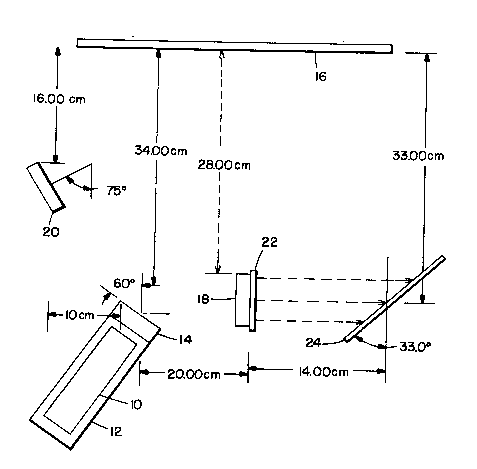
Referring to Fig. 1 an embodiment of an optical
inspection system for detecting cracks in a silicon
wafer or in intermediate layers of a solar cell is
illustrated including a laser 10 for providing a
beam of collimated illumination. Laser 10 may be a
typical HeNe laser available in the art. A video
camera 12 is disposed co-linear with laser 10 and
includes a macro-zoom lens 14. The laser 10 is
used as a guide for sighting video camera 12 at a
selected target location. Camera 12 is sensitive
to near infrared frequencies and is also available
in the art. The solar panel 16 that is to be
inspected is located in a test plane in the path of
the illumination from laser 10 and in the field of
view of video camera 12.
A first collimated light source 18, for example a
quartz halogen lamp, provides illumination 0.9 to
1.2 micron near infrared spectrum is projected
through and filtered by a long pass filter ~2 which
passes wavelengths of 1.0 micron. The filtered
collimated light from light source 18 is projected
onto the surface of white paper panel 24. The
solar panel 16 may also be illuminated by
; uncollimated unfiltered near infrared light
directed at an angle from a second quartz-halogen
light source 20. Fig. 1 includes typical
dimensions for the placement of the described
system components. These dimensions are not
critical and are included to show the compactness
- ;. . , : ' -. , : : ~ :
: . : , , ~
- . . : . - - .
.
:
21187~.~
of the system of the present invention.
The surface of the white paper 24 contains
irregularities on the order of 1.0 micron which is
also on the same order as the wavelength of the
near infrared illumination which passes through
filter 22. These irregularities cause the light
reflected from the surface of white paper 24 to
diffuse. The white paper 24 is positioned such
that the diffuse light reflected therefrom falls
upon the surface of the solar panel 16 positioned
in a test plane. Because the light rays reflected
from white paper 24 are diffuse they strike the
surface of the solar panel 16 at a plurality of
various angles.
,' :
Referring to Fig. 2, an illustration is provided
showing the light rays from lamp 18 and filter 22
``~! reflected off white paper 24 at various angles
toward solar panel 16 because of the diffuse
reflection from the white paper 24 surface.
.,
Referring to Fig. 3, an illustration is provided
~3 showing the component layers of a solar cell of
panel 16 which include the solar cell material 16A
having a metallized back surface 16B, which
supports a layer 16A of silicon germanium or a GaAs
~ material. A layer of coverglass 16D is disposed on
`~j solar cell 16A by cell adhesive 16C and a
coverglass 16E with an anti-reflective coating 16F
is located on coverglass 16D. The structure 16A,
;` 16B, 16C, 16D, 16E, and 16F in Fig. 3 depicts one
`' solar cell of the solar panel 16. Since light
,~
~c
~:'
$-
: . ' .
6 ~ 7~,~
bends at the interface between two transparent
substances with different indices of refraction,
each near infrared light ray reflected from the
diffuse surface of white paper 24 will strike the
coverglass layer 16E and be partially transmitted
through the glass at various angles according to
Snell's Law For Refraction (Ml sin 01 = M2 sin 02
where Ml is the index of refraction for the
first transparent substance.
M2 is the index of refraction for the
second transparent subs$ance.
01 is the angle of the light ray with
respect to the interface as it enters
from the first substance.
02 is the angle of the light ray with
respect to the interface as it exits into
the second substance.
The near infrared light reflected from the white
paper 24 will also strike the coverglass 16E and be
partially reflected according to the Law of
Reflection which states that the incident angle 0;
is equal to the angle of reflection 0r (0i = 0r).
~:
Thus, each individual ray of light reflected from
the white paper 24 and falling on coverglas's 16E
will consist of two subsequent rays; a transmitted
; (refracted) ray and a reflected ray. While both
reflection ~nd refraction o~ the light r~ys will
~ ,
~ . . . .
.
,~: . ' , . ' '
~ :. . ,,. : ~ .
21~7~3
occur at the interface between the coverglass 16D
- and the adhesive 16C, no total internal reflections
will occur because the light rays are travelling
into a more optically dense substance.
All of the light rays have four transitions, or
angle changes, they must undergo as they pass
through, or are reflected from, the other various
interfaces within the layers of the solar cell.
Initially each light ray must cross the interface
between the anti-reflective coating 16F and the
coverglass 16E, the interface between the
coverglass 16D and the adhesive 16C, the interface
between the adhesive 16C and the silicon wafer 16A,
and lastly the interface between the silicon 16A
and the metallized back surface 16B. All
interfaces allow for the light rays to either be
reflected or transmitted through to the next media.
Total internal reflection will only occur for
~` 20 certain light rays at the interface between air and
the anti-reflective coating 16F. As the light rays
pass through the solar cell interfaces some will be
l reflected back toward the white-paper 24, while
-~ others, as shown in Fig. 3, will be reflected in
the direction of the field of view of the camera 12
and its zoom lens 14. Those rays which fall in the
path of the field of view of the Camera 12, become
the object image from which a real image is created
and may be viewed on a control monitor (not shown)
~ 30 which is associated with the video camera 10 One
`` skilled in the art will appreciate that camera 12
may also include provision for video tape
recording, and a video graphics printer for
.
..
; ~ .
.. . . .
:.
,
.. ~ .
8 21~ 8 7l~
permanent documentation of the defe~t.
The image which is seen on the control monitor
- arises solely from the contribution of the first
collimated quartz-halogen light source 18 with its
attached Iong pass filter 22. The second light
source 20, an unfiltered uncollimated quartz-
halogen light is only used to illuminate the solar
panel 16 when it is necessary to verify whether a
detected crack is a crack in the coverglass or a
crack in the bare silicon of the cell. All
interfaces of the layers of the solar cell will
result in shadows appearing on the surface of the
silicon layer 16A, but the only two surfaces of
concern are those of the coverglass and bare solar
cell.
In Fig. 3, the dark line within the solar cell
perpendicular to the surface 16A designated by
reference number 26 indicates a crack in the bare ;
silicon and reference number 28 indicates shadows
of the actual crack 26 created by illuminating the
cracks 26 at the various interfaces.
: 25 Fig. 4 is an illustration of the various shadows
which are created in the layers of the solar cell
at the separate interfaces. Shadow 28A is at the
anti-reflective coating/coverglass interface,
shadow 28B is at the coverglass/adhesive interface,
shadow 28C is at the adhesive/silicon interfa~e and
shadow 28D is at the silicon, metallization
interface.
`I ' '.
.
! . : .,,
- ' 2ll87~3
~- The near infrared light which is used to detec~
: bare solar cell cracks and coverglass cracks comes
~- originally from the light source 18. .Both
coverglass cracks and solar cell cracks may be
viewed simultaneously at the camera. That is to
say from the view of the camera they appear to be
superimposed on top of one another, when in reality
they are on two different planes. To a trained
~ observer looking at a control monitor screen with a
: 10 picture of a cracked solar cell it would be simple
,.
to tell the difference between a coverglass crack
or a solar cell crack. Coverglass tends to shatter
or crack in a curved manner, similar to the strands
~: of a spider web. Bare solar cell will crack in 45
~ 15 or 30 straight lines depending on the crystal; orientation of the bare solar cell material. To an
untrained eye it might not be so easy to make the
clarification. Viewing is more difficult if the
~ coverglass breaks over the cell so that you have
`~ 20 both surfaces cracked but with your eye you can not
be sure if both surfaces are cracked or if it is
really just one surface. This is why the secondary
light source 20 is used; as a way to support the
determination. If the light source 20 is turned on
and you see a series of bright dots reflected back
at you on the control monitor then you know the
coverglass is definitely cracked. More
particularly, the secondary light source 20 is
turned on to verify whether or not there is any
total internal reflection of the light rays. If in
fact the light beams from the secondary source 20
e~hibit the characteristic of total internal
reflection then it determines that the ccverglass
., ~-
2 ~ ~ 8 ~ ~
is effectively cracked. This phenomenon occurs
when a single light ray strikes the crack in the
glass ~t such an angle that is either equal to or
greater than the critical angle for the interface
from the air to the anti-reflective coating on the
coverglass.
What has been described is a simple, compact and
portable test system to easily identify and
document solar cell and coverglass cracks for
accurately characterizing the reliability and
quality of the solar cells contained on a solar
panel. The present invention offers the capability
to easily verify the reliability of hardware on
site before it is launched into the space
environment. Its flexibility of use and
implementation into any sort of test station make
it not only feasible, but cost effective as well,
and thus a particularly essential asset to any
space oriented application.
.~ .
,
''`
'
i
.~ ,
~1 .
.i
.jl