Note: Descriptions are shown in the official language in which they were submitted.
211~200
BURST SRAMs FOR USE WITH A HIGH SPEED
CLOCK
The prese~t invention relates to burst SRAMs
designed to operate at a given data rate corresponding
to a first clock signal on a second, faster clock
signal.
The consumers constantly demand faster and more
powerful computers from the computer industry. A major
bottleneck in computer speed has historically been the
speed with which data can be accessed from memory,
where this speed is referred to as the memory access
time. The mi~Loplocessor, with its relatively fast
processor cycle times, has generally had to wait during
memory accesses to account for the relatively slow
memory devices. Therefore, improvement in memory
access times has been one o~ the major areas of
research in enhancing computer performance.
In order to bridge the gap between fast processor
cycle times and slow memory access times, cache memory
was developed. A cache is a small amount of very fast, -~
expensive, preferably zero wait state memory that is
used to store a copy of frequently accessed code and
data from system memory. The microprocessor can
operate out of this very fast memory and thereby reduce
the number of wait states that must be interposed
during memory accessPs.
The i486 microprocessor by the Intel Corporation
(Intel) uses a 32-bit data path and includes a version
which operates with 33 or 50 MHz clocks. The C5 or
2119200
cache controller and compatible C8 or 82490 cache
static random access memories (SRAMs) are designed for
use with the i486 microprocessor to provide a
relatively high performance microprocessor/cache system
operating at 33 or 50 MHz. Another memory chip
compatible with the i486 microprocessor is the
MCM62486A 32k X 9 BurstRAM synchronous SRAM from
Motorola, Inc., which is designed for use in a
burstable, high performance, secondary level cache for
1~ the i486 microprocessor. This particular burst SRAM
was designed to operate with a 33 MHz clock.
The P5 or Pentium microprocessor from Intel is a
next generation microprocessor offering very high
performance features, including superscaler
architecture and integrated and separate code and data
caches. One version of the P5 operates at a clock
speed of 66 MHz and uses a full 64-bit data path,
thereby providing siqnificant performance impro~ements
over the 32-bit, 33 MHz i486 microprocessor. Intel
provides a C5C cache controller with corresponding C8C
SRAMs, which provides an optimal second level cache
system for use with the P5 microprocessor. The C5C ~ . .
cache controller and C8C SRAMs, however, are very
costly. Furthermore, other design considerations and
limitations involved in the use of the C5C and C8C
cache combination make other alternatives more
attractive, especially from the standpoint of
simplicity, convenience and cost.
Standard SRAMs typically operate at 60 to 80
nanoseconds ~ns), and thus are not capable of keeping
up with the desired transfer rate of cache memory
subsystems associated with the P5 microprocessor.
Burst SRAMs capable of operating at less than 30 ns
corresponding to a 33 MHz clock ar~ desirable for use
.
2~ l~2no
with the Ps microprocessor to prevent excessive wait
states.
It is desirable to use a 66 MHz version of the P5
microprocessor in conjunction with faster burst SRAMs
designed for use with 33 MHz clock speeds, primarily
for cost and simplicity reasons. For proper operation
in systems using a microprocessor operating at a faster
speed than memory devices, however, it is typical to
provide extra clock and synchronization circuitry for
receiving the faster clock and dividing it down to a
slower clock for use by slower memory devices. The
i synchronization circuitry must insert delays so that
the memory devices are synchronized to the slower
clock. For example, it is desirable that every rising
edge of the slower clock correspond with every other
rising edge of the faster clock in a two clock system.
The faster logic, such as the CPU, may initiate
operations on any rising edge of the fast clock.
However, logic operating off the slower clock speed
must initiate operations upon the rising edge of its
slower clock. This results in substantial additional
delays in a synchronized system, since the
microprocessor may initiate a cycle on an "odd" clock
cycle, where the slower devices must wait for t.he
rising edge of the slower clock.
It is desirable, therefore, to avoid the expense
and delays of additional clock and synchronization
circuitry associated with generating and synchronizing
a slower clock signal from the sy~tem clock for use by
slower memories.
In a computer system according to the present
invention, a second level cache system is provided
using burst SRAMs designed to operat~ at a given data
2~200
rate associated with a first clock, where certain
porti~s of the burst SRAMs are capable of proper
operation using a faster clock signal but the data
cycle time is still referenced to the lower rate clock.
The timing of the registers within the burst SRAMs are
upgraded to recognize the shorter pulses of the fast
clock and control signals, although the internal memory
array is not changed. The raw data rate remains
llnch~n~ed~ but additional clock and synchronization
circuitry are unnecessary since only one primary fast
clock signal is required.
Typical burst SRAMs are designed to receive
several control signals, including an address load
signal to initiate a burst cycle, and an address
advance signal used to increment the internal address
of the RAM to continue the burst cycle. A cache
controller is provided to assert the address load and
address advance signals to receive only those clock
edges of the fast clock corresponding to a rate at
least as slow as the slower clock. Thus, only one fast
clock signal is required.
A better understanding of the present invention
can be obtained when the following detailed description
of the preferred embodiment is considered in
conjunction with the following drawings, in which:
Figure 1 is a block diagram of a burst SRAM
according the present invention;
Figure 2A is a timing diagram illustrating
operation of burst SRAMs in a lower frequency system
using a lower frequency clock;
Figure 2B is a timing diagram illustrating
operation of burst SRAMs using a lower frequency clock
in a dual clock system;
:. ' - : , :, -, . . .
, ' : -
21192~0
Figure 3 is a block diagram of the processor board
of a computer system according to the preferred
embodiment;
Figure 4 is a more detailed diagram illustrating
the connection between the memory controller of Figure
3 and the burst SRAM of Figure 1;
Figure 5 is a state machine diagram of a processor
tracker state machine operating in the memory
controller of Figure 4;
Figure 6 is a read hit state machine operating in
the memory controller of Figure 4;
Figures 7A and 7B show the logic for generating
control signals within the memo~y controller of Figure
4; and ;
Figure 8 is a timing diagram illustrating ~ -
operation of burst SRAMs according to the present
invention.
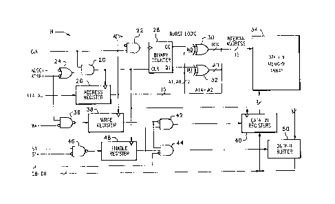
Referring now to Figure 1, a schematic block
diagram is shown of the internal portions of a 32k X 9
burst SRAM B according to the present invention. It is
noted that the basic logic portions of the block
diagram are not changed from prior art, except that
certain timing parameters are modified to allow the
burst SRAM B to operate using a faster clock signal.
The illustrated logic is that of the MCM62486A from
Motorola. As described below, the modified burst SRAM
B will operate in a similar manner with a slower clockf
and will be used with a slower clock to illustrate
operation of prior art burst SRAMs.
A clock signal CLK is provided to one input of a
two-input AND gate 20, to one input of another two-
input AND gate 22 and to the clock inputs of a write
register 38 and a data-in register 40. An address
21~2~0
advance signal ADV* is provided to an inverted input of
the AND gate 22, which has its output connected to the
clock input of a binary counter 28. An asterisk at the
end of a signal name denotes negative logic, where the
signal is true when asserted low. An address status
cache controller signal ADSC* and an address status
processor signal ADSP~ are provided to the two inverted
inputs of a two-input OR gate 24. Thus, the output of
the OR gate 24 is high when either of the ADSC* or the
ADSP* signals are asserted low. The ADSC* signal is
used as the address load signal and the ADV* signal is
used as the address advance signal.
The output of the OR gate 24 is provided to the
other input of the AND gate 20, which has its output
connected to a clear input of the binary counter 28, to
the clock input of an address register 26 and to the
clock input of an enable register 48. The address
re~ister 26 receives address bits A14-AO, which are
typically connected to a portion of the processor bus
in a computer system when the burst SRAM 8 is used for
cache memory. The output of the address register are
internal address bits IA14-IAO. The address bit IAO is
provided to one input of a two-input exclusive OR gate
30 and the IA1 address bit is provided to one input of
another two-input exclusive OR gate 32. The least
significant bit (LSB) output of the binary counter 28
is provided to the other input of the exclusive OR gate
30, and the most significant bit (MSB) of the binary
counter 28 is provided to the other input of the
exclusive ~R gate 32. The address bits IAl4-IA2 from
the address register 26 are provided to the upper 13
address bits of an internal 32Kx9 memory array 34
provided within the burst SRAM B. The output of the
exclusive OR gate 30 is an address bit IA'O provided to
bit O of the address input of the memory array 34,
.
.
, : ., ~ , ....
21 1~200
whereas the output of the exclusive OR gatP 32 provides
an address bit IA'l to the bit 1 address input of the
memory array 34. The signals IA14-IA2, IA'1, IA'0 form
an internal address of the burst SRAM B. When the
binary counter 28 is clocked, the IA'O and IA'1 bits
are used to increment the internal address.
The ADSP* signal is provided to one input of a ~ -
two-input NAND gate 36, which has an inverted input
connected to a signal W*. The output of the NAND gate
36 is provided ~o the input of the write register 38,
which has its output connected to the inverted input of
a two-input AND gate 42 and to a non-inverted input of
a three-input AND gate 44. A first chip select input
signal so is connected to the non-inverted input of a
two-input AND gate 46 and another chip select input
signal S1* is connected to the inverted input of the
AND gate 46, which has its output connected to the
input of the enable register 43. The output of the
enable register 48 is provided to the non-inverted
input of the AND gate 42 as well as a second non-
inverted input of the AND gate 44. The inverted input
of the AND gate 44 is connected to an output enable
input signal G*.
The output of the AND gate 42 is connected to the
enable input of data-in registers 40, which receive the
D8-DO data bits. The data-in registers 40 have outputs
connected to the data inputs of the memory array 34.
The output of the AND gate 44 is provided to the enable
input of an output buffer 50, which receives the data
output of the memory array 34 at its input, and has its
output connected to the D8-D0 data bits.
The operation of the burst SRAM B will be
described as used in the memory portion of a second
level cache subsystem. An array or matrix of burst
SRAMs similar to the burst SRAM B would preferably be
2il9200
8-
used to comprise the cache memory for the second level
cache. The particular configuration would depend on
the width of the data bus and the amount of memory
desired. The S0 and Sl* signals are assumed asserted
for simplicity. The clock input CLK is preferably
- connected to the processor clock. A cache controller
(not shown) provides an address load signal to the
ADSC* signal input, an address advance signal to the
ADV* signal input, an output enable input signal to the
G* signal input and a read/write signal to the W*
signal input. A microprocessor would typically provide
the ADSP* signal. The address bits A14-A0 and data
bits D8-D0 are connected to corresponding portions of
the processor bus, although D~ is usually a parity bit
for the data bits D7-Do.
The ADSC* signal is asserted low, causing the
address register 26 to be clocked on the rising edge of
the CLK signal, strobing in an address from the
proces~or address bus to the memory array 34. The
enable register 48 and the write register 38 are also
clocked, thus effectively enabling the AND gates 42 or
44 depending upon the W* and G* signals. If the ADV*
signal remains negated high, the binary counter 28 is
not clocked so that the IA'0 and IA'1 address bits
mirror the IA0 and IA1 address bits, where the address
indicated from the processor bus is provided directly
to the memory array 34. If a write cycle is indicated
by the W* signal asserted low, the data-in registers 40
are enabled so that the data from the processor bus is
provided to the memory array 34. If a read cycle is
indicated, data from the memory array 34 is provided to
the input of the output buffer 50, which is then
provided to the processor bus when the G* signal is
asserted low.
~, : ,-..... . .
.:,: .
21192~0
The memory array 34 essentially defines the data
rate for both the data read and write cycles. Thus,
even though an address is provided early, the data is
not fully stored in a write cycle, or is not valid for
a read cycle, until enough time has elapsed as
specified by the manufacturer.
Even~ually, read data bec_ -c valid for assertion
on the processor bus, or write data is accepted by the
memory array 34 from ~he data-in registers 40. The
ADV* signal is then asserted low so that the binary
counter 28 is clocked on the subsequent rising edge of
the CLX signal. Clocking the binary counter 28 causes
the internal address to be incremented to point to the
next consecutive address location of the memory array
34. While the ADV* signal remains asserted low,
subsequent rising edges of the CLK signal clock the
binary counter 28, thereby incrementing the internal
address to the memory array 34. After the last rising
edge of the CLX signal in a burst cycle, the ADV*
signal is negated so that remaining CLK cycles are
ignored. It is noted that the ADV* signal may be
negated during the burst cycle to ignore the CLX
signal, thus suspending operation. The ADV* signal
would then be asserted low to complete the burst cycle.
The block diagram shown in Fig. 1 is substantially
the same for burst SRAMs of prior art. Only the timing
is changed. Effectively, the binary counter 28 and the
registers 26, 38, 40 and 48 are designed to be capable
of receiving faster clock and control pulses for
latching the data, such as those occurring with a 66
MHz pulse having high and low times of approximately 7
ns. The primary speed of the memory array 34 remains
substantially unchanged, in the preferred ~mho~ir~nt 20
or 25 ns conforming to an effective 33 MHz data rate.
2119200
.
:::
Referring now to Figure 2A, a timing diagram is
shown illustrating operation of the burst SRAM B
operating at its normal clock rate, which is preferably
33 MHz. It is noted that although the burst SRAM B is
capable of receiving a faster clock, it uses a slower
clock to demonstrate the operation of prior art burst
SRAMs. In a typical ~mho~; -nt, a microprocessor, such
as the i~86 microprocessor by Intel, includes an ADS*
ou'put signal to initiate the beginning of a read/write
cycle. The burst SRAM B is specifically designed for
use with the i486 microprocessor so that the ADS*
signal from the processor bus is tied directly to the
ADSP* signal. A separate cache controller (not shown)
would be provided and connected to the clock, the ADS*
signal, the address bus and other control signals of
the i486 microprocessor, where the cache controller
would provide the ADSC*, W*, C* and ADV* signals to the
burst SRAM B.
As shown in Figure 2A, a first clock signal PCLK
is shown which preferably operates at a rate of 66 MHz,
where a rising sdge occurs at times TO, T2, T4, T6, T8
and so on. A second, slower clock signal referred to
as DCLK, operates at half the speed of the PCLX signal
or 33 MHz, so that a rising edge occurs at times TO,
T4, T8, T12 and so on. It is understood that although
the clock frequencies illustrated are different by a
factor of two, the present invention may be practiced
with a high frequency clock signal at any integer
factor of the slow clock frequency, as long as the
burst SRA~ B is capable of detecting the shorter
pulses. A factor of two is used for purposes of
simplicity.
In a typical burst SRAM used in conjunction with
an i486 microprocessor, the 33 MHz clock signal DCLK
signal is used for all operations. After a slight
.. . . , ., . ~ , . ........ . .
. . -- ~ : . : -
2119200
11
delay from time T0, the ADS* signal is asserted low and
remains low for approximately a full DCLK signal clock
cycle. The ADS* signal is detected asserted low at the
rising edge of the DCLK signal at time T4. Thus, at
time T4, the burst SRAM has sampled the address from
the processor address bus and begins to assert the
corresponding data after a slight delay from time T4.
The ADV* signal is also asserted low after a delay from
time T4 in order to internally advancç the address
during the burst cycle. The ADV* signal remains
asserted low for approximately three DCLR signal cycles
during the burst read cycle if the burst read cycle
continues uninterrupted. Thus, one DCLK signal cycle
later at a time T8, the rising edge of the DCLK signal
is sampled by the binary counter 28 and the internal
address is incremented. After a slight delay from time
T8, new data is asserted from the burst SRAM onto the
processor data bus.
One DCLK signal cycle after time T8 at a time T12,
the ADV* signal is still asserted low so that the
rising edge of the DCLR signal is detected by the
binary counter 28 at time T12. Again, the internal
address is incremented so that new data is asserted a
short delay period after time T12. Approximately one
cycle of the DCLK signal later, at time T16, the ADV*
signal remains asserted so that the rising edge of the
DCLK signal is detected at time T16, thereby
incrementing the internal address of the burst SRAM B
again. The fourth set of data is subsequently asserted
onto the processor data bus, which is the last set of
data in the burst read cycle. The ADV* signal is
negated after time T16 to prevent latching any further
addresse~ from the processor address bus unless another
cycle is p~n~ing. The duration of the burst read cycle
from assertisn of the ADS* signal until the last da~a
2119200
12
segment is provided is between 5 and 6 DCLK signal
cycles in a 33 MHz system.
Referring now to Figure 2B, the same burst SRAM B
used for Figure 2A is used except in a system
incorporating a faster processor, such as the P5
microprocessor from Intel, which preferably operates at
66 MHz. Separate clock and synchronization circuitry
(not shown) must be provided to receive the PCLK signal
and provide the DCLK signal in order to operate the
burst SRAMs of prior art, since they may only operate
at a slower clock frequency. The synchronization
portion may be provided in a cache controller since a
cache controller would typically be required to operate
the cache memory. The clock and synchronization
circuitry must perform synchronization and clock
delaying operations, since the pulses provided from the
faster microprocessor may not be provided directly to
the burst SRAMs. The clock circuitry must provide
appropriate delay in case operation of the faster logic
is initiated on an "odd" PCLX signal cycle relative to
the DCLK signal. The ADS* signal may not be directly
tied to the burst SRAMs since they are unable to
operate with the faster pulses. In this case, the
ADSP* signal is pulled high and the ADSC* signa' is
used to load or strobe in the data.
In Figure 2B, the microprocessor asserts the ADS*
signal at approximately time T0, where the ADS* signal
is negated approximately one PCLK signal cycle later at
time T2. The clock and synchronization logic detects
the ADS* signal asserted and asserts the ADSC* signal
at time T4. The clock circuitry asserts the ADSC*
signal for a duration of about one DCLK signal cycle
between time T4 and time T8. The clock circuitry then
asserts the ADV* signal at approximately time T8 in a
similar manner as shown in Figure 2A, where the ADV*
: ": . -, , . - :
~",'' ~ ' ' .
:. . . .
:
;"
",- . .
,. . . .
211~2~
signal remains asserted for approximately 3 DCLX signal
cycles to time T20. Data segments are shown asserted
on the data bus processor beginning at time T8 and
ending at time T24. Although the cycle operates
substantially the same as that shown in Figure 2A for
an i486 mi~o~-ocessor system, the entire burst read
cycle is stretched for one DCLK signal cycle since the
A~S* signal is not provided directly to the burst SRAM,
and the cycle was initiated on an "odd" PCLK signal
cycle not c~..ea~onding to the rising edge of the DCLK
signal.
Even if the microprocessor asserts its ADS* signal
to begin a new cycle at an even PCLK signal cycle ;
relative to the DCLK signal, one PCLX signal cycle
delay is still necessary to properly synchronize the
burst SRAMs with its slower clock signal. As shown in
Figure 2B, the ADS* signal is again asserted at
approximately time T22, which corresponds with a
falling edge of the DCLK signal. The clock and
synchronization circuitry asserts the ADSC* signal at
time T24, which occurs one PCLX signal cycle sooner
than the first burst cycle. Thus, the ADSC* signal
remains asserted until after time T28, approximately
one DCLK signal cycle later. After a short delay from
time T28, the ADV* signal is asserted low and remains
asserted until approximately time T40, when the last ~
DCLK signal rising edge is sampled, incre~enting the ~ -
addresa as described previously. Thus, the cycle
operates in a very similar manner as the first case
shown in Fig. 2h except that one PCLK signal cycle of
delay is saved. In either case, the entire burst read
cycle is at least one PCLK signal cycle longer in
duration than that for the i486 system due to
synchronization required in a two-clock system.
.. :.: . . : . . .. : ..
2~192~0
14
Referring now to Figure 3, a block diagram of a
processor board P implemented according to the present
invention is shown. The remaining system and I/0
portions of the computer system are not necessary for
full disclosure of the present invention, and thus are
not shown or described for purposes of simplicity. The
primary component on the processor board P is a central
processing unit (CPU) 52, which is preferably the P5
microprocessor from Intel. Three buses are connected
to the CPU 52, including the PD or processor data bus,
the PA or processor address bus and the PC or processor
control bus. A second level cache memory, otherwise
referred to as the L2 cache 54, is connected to the PD
and PA buses and receives several control signals from
a memory controller 56. In the preferred embodiment,
the memory controller 56 contains conventional memory
controller functions and additionally includes the
cache controller capabilities necessary for interfacing
the L2 cache 54.
A data buffer 58 is connected to the PD bus and
develops two new buses, the HD or host data bus and the
MD or memory data bus. The HD bus is part of a host
bus H, and is connected to a connector 80 for
connection ~o the system board (not shown) of the
computer system. The data buffer 58 is controlled by
the memory controller 56. A transceiver/latch unit 60
is connected between the PA bus and the HA bus to
provide latching and transceiving capabilities of
addresses between the CPU 52 and the host bus H. The
transceiver/latch 60 is controlled by the memory
controller 56. The memory controller 56 is connected
to a unit referred to as the DDF or data destination
facility 64. The DDF 64 performs memory module
enabling, address translation and memory segment or
page property storage.
211.~2~0
A processor utility chip 62 provides certain
necessary utility operations for use with the CPU 52.
The processor utility chip 62 is connected to an XD
bus, the host bus H and is controlled by the memory
controller 56. The output of the processor utility
chip 62 is preferably provided to the PC bus to provide
control functions of the CPU 52. : ~ :
The memory portion of the processor board P is
provided as four identical modules, each module
cont~;n;ng an address/control buffer 66, one socket for
receiving an individual SIM~ unit 68 and base memory
70. The address/control buffer 66 receives the PA bus,
the address and enable outputs of the DDF 64 and ~ ;
control signals from the memory controller 56. The
outputs of the address/control buffer 66 are the
addresses provided to the SIMMs 68 or base memory
devices 70. As indicated, there are four like modules.
Other configurations of the processor board P could be
developed, with variations obvious to one skilled in
the art.
The CPU 52 operates in a similar manner as the
i486 microprocessor, where it asserts an address status :~
signal ADS* indicating that a new valid bus cycle is
currently being driven by the CPU 52. When the ADS*
signal is asserted, the CPU 52 also drives a signal
M/IO* indicating whether the cycle is a memory or I/O
operation, a signal W/R* indicating whether the cycle
is a write or a read operation and a signal D/C*
indicating a data or control cycle. The CPU 52 also
asserts eight byte enable bits BE7*-BE0* indicating
which bytes of the PD data bus are to be read or
written by the CPU 52. In general, the cycle is
terminated by an external device asserting a burst
ready signal BRDY* to the CPU 52, indicating that the
external device has presented valid data for a read
211~200
16
cycle or has accepted data in response to a write
request. The CPU 52, however, also supports address
pipelining, which is not supported by the i486
microprocessor, where the next cycle may begin before
the data phase of the previous cycle is completed. An
external device asserts a next address signal NA*
indicating its preparedness to begin a new cycle. The
CPU 52 may thus begin a new cycle by asserting the ADS*
signal before or on the same clock cycle as when the
BRDY~ signal is asserted.
Referring now to Figure 4, a more detailed
schematic diagram is shown illustrating the connection
between the memory controller 56 and the burst SRAM B,
where the burst SRAM B is preferably one of eight
similar burst SRAMs within the L2 cache 54.
Preferably, the L2 cache 54 is a relatively simple 256
kbyte, direct-mapped, lookaside, write-through cache
for simplicity of logic and operations. The memory
controller 56 provides signals CADSC*, CADV*, CW*, and
CDROE* which are connected to the ADSC*, ADV*, W* and
GC* signals, respectively, of the burst S~AM B. In the
preferred ~mhod; ?nt, the CADSC* and CADV* signals
actually comprise A and B versions for buffering and
clock fan-out purposes, but only one signal is
described for simpli~ity since these signals are
similar in operation. The CW* signal is derived from
the W/R* signal from the CPU 52 and the CDROE* signal
is simply an output enable signal as known to those
skilled in the art.
The PCLK signal is provided to both the memory
controller 56 and the burst SRAM B. The burst SRAM B
is connected to bits PA17-PA3 of the processor data bus
PD. Data bit D8 is preferably a parity error bit
provided to a separate processor data parity bus PDP.
The ADSP* and SO input signals are preferably pulled
~ : : ,: : . -
21 192 ~0 ~ ~
high through a pull-up register 72, and the SI* input
signal is pr~fera~ly pulled down to ground through a
pull-down resistor 74.
The logic within the memory controller 56 for
5 performing the cache controller functions used to ~-
develop the CADSC* and CADV* signals will now be
described. Referring now to Figure 5, a state machine
diagram is shown illustrating the operation of a
proc~sor tracker state machine (P5TRRSM) implemented
lo within the memory controller 56 of Figure 4. The
P5TRKS~ is advanced ~rom one state to the next on the
positive edge of the PCLK signal. Upon reset of the
computer system, the P5TRRSM enter~ a state P0, where a
signal P0 is also asserted to other state machines
within the memory controller 56 during state P0. The
P5TRKSM remains in state P0 as long as a signal CPADS
signal remains negated. A tilde sign "~" indicates
logical negation. The C~ADS signal is the ADS* signal
which has been synchronized to the PCLK signal clock
signal and inverted. When a valid cycle is initiated
on the processor bus from the CPU 2, the CPADS signal
i5 asserted and the P5TRKSM advances to state P1 upon
the next rising edge of the PCLK signal. A
COL~eS~Ollding signal P1 is asserted by the P5TRK~M
during state P1. From state Pl, operation advances to
state P2 on the next rising edge of the PCLX signal,
where a corresponding signal P2 is asserted while in
state P2. The CPADS signal and a signal LBRDY
determine which state the ~ ~K~ advances to on the
next rising edge of the PCLK signal.
The LBRDY signal depPn~c on many other signals and
corresponds to the last BRDY* signal, indicating data
has been accepted or valid data is being provided for
each data cycle. The following equations define the
LBRDY signal
: . ', ~ :
211920~
18 -
LBRDY= P~OC ~ CPRDY
CPRDY:= CRDY + EPBRDY
CRDY= L2CACHE_ON ~ Pl ~ MEMRD ~ RDHIT A -
-NOCHIT ~ CHIT + RDHIT_C + FLUSHRDY
L2CACHE ON := SYNC_CACHEN ~ CL2EN ~ NOCACHE
where the ":=" signal indicates a registered condition
so that the signal on the left side of the equation is
true when the conditions on the right side are true at
the positive edge of the PCLX signal. The "~" signal
indicates the logical "OR" function. It is significant
to note that the LBRDY signal is asserted on the first
positive edge of the PCLK signal after the PEOC and
CPBRDY signals are asserted, indicating the last clock
cycle of the current processor cycle. The PEOC signal
indicates the end of a processor cycle and is developed
by other logic in the memory controller 56. The CRDY
signal is a cache ready signal and is provided o~e PCLK
signal cycle early on memory controller 56 handled
transfers.
The MEMRD signal is true when a signal PMIO
indicates a memory cycle and a signal PWR indicates a
read cycle. The PMIO and PWR signals are latched and
inverted versions of the M/IO* and W/R* signals
asserted by the CPU 52. The RDHIT_A signal indicates
that a read hit state machine (RDHITSM), described
below, residing within memory controller 56 is
indicating read hits to the L2 cache 54 and is in the
initial state. A RDHIT_C signal is provided by the
RDHITSM indicating that bursted read cycles are in
progress and that read hits are occurringO
The SYNC CACHEN signal is a registered version of
a signal CACHEN, which is bit 6 of a RAM setup port
located at memory addres~ ~0C00002h. The CACHEN signal
is also bit 2 of a processor control port, which
211 9200
19
mirrors bit 6 of the RAM setup port. The RAM setup
register is used to enable a primary cache within the
CPU 52 and the L2 ca~he 54, and also contains system
status and control bits. The processor con~rol port
contains miscellaneous processor and numeric
coprocessor functions. In this manner, the CACHEN
signal is used to disable both caches. Thus, the
L2CACHE_ON signal indicates that the L2 cache 54 is ;
installed and enabled. The FLUSHRDY signal is asserted
by a flush state machine (not shown) within the memory
controller 56, where the FLU5HRDY signal is used to
develop the BRDY* signal to the CPU 52 after flushing
the L2 cache 54.
The P5TRKSM remains in state P2 while the CPADS
and LBRDY signals remain negated. If the CPADS signal
remains negated and the LBRDY signal is asserted, the
state machine advances back to state P0 indicating the
end of a non-pipelined cycle. If the CPADS and LBRDY
signals are both asserted during state P2, indicating a
pipelined cycle present and the prior cycle completing,
operation advances back to state Pl. If the CPADS
signal is asserted while the LBRDY signal remains
negated in state P2, also indicating a pipelined cycle
but without completion of the prior cycle, operation
proceeds to state P3, where a corresponding signal P3
is asserted~ Operation remains in state P3 while the
LBRDY signal is negated. When the LBRDY signal is
asserted in state P3, operation advances back to state
P2. Thus, the P5TRKSM essentially tracks the cycles
executed by the CPU 52 to determine the start and the
completion of each processor cycle.
Referring now to Figure 6, a state machine diagram
is shown illustrating the operation of the RDhl~L~
state machine operating within the memory controller 56
of Figure 4. The RDHITSM is simplified since several
- : . .
2~192~
other states and other logic have been omitted as not
necPssary for full disclosure of the present invention.
The RDHITSM is advanced on the rising edges of the PCLK
signal. The RDHITSM remains in state A until a memory
read occurs as indicated by the MEMRD signal, a cache
hit occurs as indicated by the CHIT signal asserted and
the NOCHIT signal not asserted, the L2 cache 54 ls
installed and enabled and the P5TRKSM state machine is
in state P1. When these conditions are met, the
RDHITSM advances to state B. Otherwise, the RDh~
remains in state A as indicated by an ELSE loop. In
state B, the RDHITSM asserts a signal RDHIT_ B.
From state B, operation proceeds to state C if the
LBRDY signal is not asserted indicating it is not the
last BRDY* clock cycle in a burst, or if the LBRDY
signal is asserted, a memory read is indicated, a cache
hit has occurred and the P5TRKSM state machine is in
state P3. A signal LCHIT is a latched version of the
CHIT signal. If these conditions are not met, the
RDHITSM returns to state A indicated by an ELSE branch.
During state C, the RDHITSM asserts the RDHIT_3 signal,
which is used to derive the CADV* signal. From state
C, operation always proceeds to state B on the next
rising edge of the PCLK signal.
Referring now to Figure 7A, a schematic diagram is
shown illustrating the logic used to develop the CADSC*
signal. A two-input multiplexor 82 receives a signal
CMFADS* at its A input and the ADS* signal at its B
input. A signal CADSMUX is provided to the S select
input, where the A input, or the CMFADS* signal, is
provided at the Z output when the CADSMUX signal is
false, and the B input, or the ADS* signal, is provided
to the Z output when the CADSMUX signal is true. The Z
output is provided to the D input of a D-type flip-flop
84, which receives the PCLK signal at its clock input.
- ~ ... .
.
.,
21192~0 : ~
The Q output of the D-flip-flop 84 provides the CADSC*
signal through a delay buffer 86. The Q* output
provides a signal ICADS. The following equations
define the state of t~e CMFADS* and CADSMUX signals:
CMFADS* = ~(P0 ~ CPADS ~ -ICADS + P2 ~
RDHIT_C ~ PEOC ~ CPADS + P3 -
RDHIT_C ~ PEOC ~ D_CADS ~
-INH_CADS~
D_CADS := P2 ~ CPADS ~ LBRDY + P3 ~
LBRDY
INH_CADS := RDHIT_B ~ PEOC ~ ICADS
CADSMUX = P0 ~ -CPADS + P2 ~ CPADS -
(RDHIT C + RDHIT_B) ~ PEOC
According to Figure 7A and the above equations,
the ADS* signal is used to initiate an assertion of the :
CADSC* signal to the burst SR~M B during the next PCLR
signal cycle in a non-pipelined cycle. In a pipelined ::
cycle where the ADS* signal is asserted early, the
CMFADS* signal is used instead to delay the assertion
of the CADSC* signal until the previous cycle is
completed.
Referring now to Figure 7B, a schematic diagram is
shown illustrating the logic used to develop the CADV*
signal. A signal NCADV is inverted by an inverter 88
and the inverted signal is provided to the D input of a
D-type flip-flop 90. The PCLK signal is provided to
the clock input of the D flip-flop 90. The Q output of
the D flip-flop 90 provides the CADV* signal through a
delay buffer 92. The NCADV signal is defined by the
following equation:
NCADV = L2 Q CHE_ON ~ Pl ~ T~RnATTOC -
-NOCHIT ~ CHIT + RDHIT_C ~ -PEOC
21192DO
where the T.7~n~T.T~C signal is true if a cacheable
memory read is occurring and both the internal cache of
the CPU 52 and ~he L2 cache 54 are enabled. In brief,
the NCADV signal is true during a cacheable read hit
cycle when the P5TRKSM is in state P1, or when the
RDHITSM ls in state C and the PEOC signal is not
asserted. The CADV* signal is asserted during the PCLK
signal cycle following the assertion of the NCADV
signal.
~0 Referring now t~ Figure 8, a timing diagram is
shown illustrating a cache read hit cycle. Again, the
PCLK signal is operating at a frequency of 66 MHz. A
read hit cycle is shown to illustrate the operation of
the present invention. Other types of cache cycles
occur in the preferred ~mho~; mPnt~ such as read
allocate, line fills or write-back cycles, which are
not shown or described for purposes of simplicity. The
ADS* signal is asserted at time T0 while the P5TRKSM is
in stat~ Po and the RDHITSM is in state A. One PCLR
signal cycle later, the ADS~ signal is negated and the
CADSC* signal is asserted low to the burst SRAM.
Again, the P5TRKSM remains in P0 and the RD~llS~
machine r~ i nc in state A. On the next rising edge of
the PCLX signal at time T4, the CADSC* signal is
negated and the P5TRKSM is advanced to state P1,
whereas the RDHITSM remains in state A. At time T6,
one PCLK signal cycle later, the CADV* signal is
asserted and the P5TRXSM advances to state P2 while the
R~nll~M advances to state B. The BRDY* signal also is
asserted synchronous with state B of the R~ M. The
first set of data from the burst SRAM B is now
available to the processor data bus PD during this PCLR
signal clock cycle.
On the following rising edge of the PCLK signal at
time T8, the CADV* signal is negated while the P5TRKSM
,
.. , . . . , -
2~ 1~200
23
remains in state P2 and the RDHITSM machine advances to
state C. At time T10, the BRDY* and CADV* signals are
asserted while the P5TRKSM remains in state P2 and the
RDHITSM advances back to state B. At this time, the
5 second set of data is provided on the processor bus PD
for one PCLK signal cycle. At time T12, the BRDY* and
CADV* signals are negated while the PSTRKSM remains in
state P2 and the RDHITSM advances to state C. At time
T14, the BRDY* signal and the last CADV* signal is
asserted while the PsTRKSM remains in state P2 and the
RDHITSM advances back to state B. At this time, the
third data group ~e~ -~ valid on the processor data
bus PD.
At time T16, the BRDY* and CADV* signals are
negated while the P5TRKSM remains in state P2 and the
RDn~ advances to state C. Also, the PEOC signal is
asserted while the RDHITSM is in state C, so that the
CADV* signal is not asserted during the following PCLK
signal cycle. At time T18, the BRDY* and LB~DY signals
are asserted, indicating the last data clock cycle o~
the burst cycle. The P5TRKSM remains in state P2 while
the RDh~ advances back to state B and the last set
of data is provided on the processor data bus PD. The
cycle ends at time T20 when the BRDY* and the LBRDY
signals axe negated, the P5TRXSM advances to state PO
and the RDHITSM returns to state A.
It is noted that during a burst read hit cycle,
the RD~l~ advances from state A to state B to state C
and alternates between states B and C on consecutive
rising edges of the PCLX signal since the LBRDY signal
is not asserted until the last BRDY* signal is
asserted. The CADV* signal is asserted during state B
and thus asserted every other clock cycle of the PCLK
signal. In this manner, the CADV* signal is asserted
then negated on consecutive rising edges of the PCLK
..
. ~ . ,
,..... ' . ' ,, : ' ~
: . .
!.," ' . - ~ . : . . ~
,'
21~9200
24
signal, so that the internal address of the burst SRAM
B is advanced on every other rising edge of the PCLK
signal. In this manner, the burst SRAMS effectively
operates at a 33 MHz rate using the 66 MHz clock. In
comparison with Figures 2A and 2B, the duration of the
cycle from assertion of the ADS* signal to the last
data segment available is 10 PCLK signal cycles
(equalling 5 DCLK signal cycles), which is the same
rate as the burst SRAM B tied directly to the i486
microprocessor, and at least one PCLK signal cycle
~aster than the two clock system illustrated in Fig.
2B.
It can now be appreciated that a computer system
using burst SRAMs according to the present invention
may use a microprocessor operating at a higher clock
frequency in conjunction with cache memory operating at
a lower clock frequency without requiring the lower
frequency clock signal. ~he burst SRAM B operates at
the same data rate as used in systems using the slower
clock frequency, but is capable of receiving the higher
frequency clock. Cache controller logic provides the
address load and advance signals corresponding to every
other clock pulse of the high ~requency clock, and
suppressing every other clock pulse to the burst SRAM
B. In this manner, additional clock generation and
synchronization circuitry used to develop the slower
clock i5 not required and the delays which necessarily
result can be avoided, t~us increasing system
perfo- nce while allowing the use of lower cost burst
SRAMs.
The foregoing disclosure and description of the
invention are illustrative and explanatory thereof, and
various changes in the size, shape, materials,
components, circuit elements, wiring connections and
contacts, as well as in the details of the illustrated
; , - , . . ... . .
2~ 1~2~0 ~
circuitry and construction and method of operation may
be made without departin~3 from the spirit of the
invention .
.
~ , .
':