Note: Descriptions are shown in the official language in which they were submitted.
2119228
ARRANGEMENT FOR EXPANDING THE DEVICE CAPACITY OF A BUS
Technical Field
This invention is directed generally to communications buses, and is
directed specifically to the SCSI peripheral bus.
S Back~round of the Invention
The Small Computer System Interface (SCSI) input/output (I/O) bus is
widely-used to connect peripheral devices, such as input and output interface devices
and mass storage devices (e.g., disks and tapes), to small and medium-size
computers, including to workstations and personal COml)Utel S (PCs). As the
10 complexity of applications that these compulels support increases along with their
power, there is arising a need to connect these colllpu~,~ to ever-more peripheral
devices. Furthermore, as these computers come to support more mission-critical
applications, the need for highly-reliable configurations (e.g., duplicated or
re~lilnd~nt configurations) is becoming pronounced.
Unfortunately, the SCSI bus is not well suited to meet these needs. The
standard SCSI bus has an addressing limit of eight device identifiers (IDs) ànd hence
is limited to having only eight peripheral devices connected thereto. This number is
reduced to only four distinct duplicated devices in a fault-tolerant application that
relies on active-device redundancy. Furthermore, the SCSI bus standard requires
20 each device ID to be unique.
Summary of the Invention
This invention is directed to solving these and other problems and
disadvantages of the prior art. Illustratively according to the invention, there is
provided a bank-switching scheme that allows banks of duplicate devices on the
25 SCSI bus to share SCSI device IDs. Control circuitry selects and communicatively
connects to the bus only one of the banks of devices, and -- if a plurality of host (i.e.,
bus master) devices are present -- only one of the hosts at any one time, while
keeping the other banks and hosts cornmunicatively disconnected from the bus.
Generally according to the invention, in an apparatus that comprises a
30 communications medium, such as a SCSI bus, a first active (e.g., enabled)
addressable device connected to the medium, and a second active addressable device
connected to the medium, wherein both active devices have the same address on the
medium, there is included a selection arrangement coupled to the two devices, for
enabling only one of the active devices at any one time to receive their common
35 address on the medium. The others of the active devices are prevented from
receiving their common address on the merlillm at the one time. Preferably, the
-2~ 2 2 8
selection arrangement comprises a plurality of means each connecting a
corresponding device to the medium, and each for selectively either (a)
communicatively coupling the corresponding active device to the medium or (b)
communicatively uncoupling the corresponding active device from the medium, at
any one time.
Advantageously, the arrangement allows active devices to share addresses
on the medium, yet allows for selection of only one of the active devices that are
sharing an address to be reached via, and respond to, that address at any one time.
Hence, more active devices than there are unique device addresses may be
connected to the medium. Thus, for example, more than eight active devices may
be connected to a SCSI bus. The arrangement also preferably and advantageously
communicatively uncouples all but one of the active devices that share an address
from the medium in such a manner that the increase in the number of active
devices that can be connected to the medium does not adversely affect the electrical
characteristics of the medium. Hence, the arrangement facilitates either an increase
in the number of distinct active devices, or a duplication of active devices without
a corresponding decrease in the number of distinct active devices, that can be
connected to the medium. Yet it does so without violating the SCSI standard.
Further preferably, the apparatus includes a plurality of hosts, each for
communicating with the devices on the medium9 and a selective coupling
arrangement that connects the plurality of hosts to the medium but
communicatively couples only one of the plurality of hosts to the medium at any
one time. This configuration permits the medium to be used in a fault-tolerant
apparatus, wherein the devices and the host are both replicated for reliability. For
example, the invention supports use of the SCSI bus in an on-line/off-line host-processor configuration, again without violating the SCSI standard.
In accordance with one aspect of the invention there is provided an
apparatus comprising: a SCSI bus; a plurality of device banks connected to the
SCSI bus for communicating on the SCSI bus, each device bank comprising a
plurality of active devices, the active devices of one device bank having same SCSI
- 2a~ 2 ~
addresses on the SCSI bus as the active devices of the other device banks; and
selection means coupled to the plurality of device banks, for enabling the active
devices of only one of the plurality of device banks at any one time to receive the
SCSI addresses on the SCSI bus while preventing the active devices of the othersof the plurality of device banks at the one time from receiving the SCSI addresses
on the SCSI bus.
In accordance with another aspect of the invention there is provided a
method of operating an apparatus comprising a communications bus and a pluralityof device banks each comprising a plurality of active addressable devices connected
to the communications bus for communicating on the communications bus, the
active addressable devices of one device bank being addressed by the same
addresses on the communications bus as the active addressable devices of the other
device banks, comprising the steps of: in response to receipt of a device bank
selection signal, enabling the active addressable devices of only a selected one of
the plurality of device banks at any one time to receive, and thus be addressed by,
addresses-on the communications bus; and in response to said receipt, preventingthe active addressable devices of the others of the plurality of device banks at the
one time from receiving, and thus being addressed by, addresses on the
communications bus.
These and other advantages and features of the invention will become
more apparent from the following description of an illustrative embodiment of the
invention taken together with the drawing.
Brief Description of the Drawing
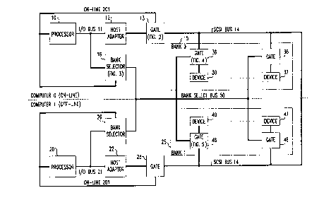
FIG. 1 is a block diagram of an illustrative computer system that includes
an illustrative embodiment of the invention;
FIG. 2 is a block diagram of a host adapter gate of the system of FIG. 1;
FIG. 3 is a block diagram of a bank selector of the system of FIG. 1;
2119228
- 3 -
FIG. 4 is a block diagram of a device gate of device bank 0 of the
system of FIG. l; and
FIG. 5 is a block diagram of a device gate of device bank 1 of the
system of FIG. 1.
S Detailed Description
FIG. 1 shows an illustrative fault-tolerant SCSI-based computer system.
The shown computer system comprises a pair of compulels, con~l)uler 0 and
computer 1, that mirror each other and operate in conventional active-standby
redund~ncy mode. Illustratively, co--lpuler 0 is presently designated as the on-line
10 computer and computer 1 is presently designated as the off-line, or standby,
COIl~l~ul~l.
Each computer 0,1 includes a conventional processor 10,20 such as a
workstation or a PC, connected by means of an VO bus 11,21 and a host
adapter 12,22 to a SCSI bus 14. SCSI bus 14 is connected to a plurality of peripheral
15 devices 30-37,40-47. These devices are assumed to include the conventional
interface Cil~ y for connecting to a SCSI bus. Devices 30-37 illustratively
duplicate devices 40-47 both in type and in data content. All devices 30-37, 40-47
are active, e.g., enabled, except during special circumstances such as device failure.
According to the invention, devices 30-37 form one bank 15 of devices,
20 designated as bank 0, while devices 40-47 form another bank 25 of devices,
designated as bank 1, and only one of the two banks 15,25 of devices is addressable,
and hence accessible, via SCSI bus 14 at any one time. Which bank 15,25 is
presently accessible is controlled by the on-line one of the processors 10,20 bymeans of a bank select bus 50. Each device 30-37,40-47 of a bank 15,25 is coupled
25 to SCSI bus 14 by its own gate 38,48, and bus 50 controls all gates 38,48 of a
particular bank 15,25 in tandem so as to communicatively couple or uncouple thatbank's included devices 30-37,40-47 to or from SCSI bus 14 simult~neously. A
bank-selection operation performed across bus 50 must precede the SCSI bus
operation (e.g., device access) of interest.
Each processor 10,20 has an associated bank selector 16,26 that
interfaces that processor's VO bus 11,21 to bank select bus 50. Only the on-lineprocessor's bank selector is active at any one time, thereby perrnitting only the
presently-on-line processor to control bank selection. Similarly, only the on-line one
of the processors 10,20 has access to SCSI bus 14 at any one time. Each processor's
35 corresponding host adapter 12,22 is interfaced to SCSI bus 14 by a gate 13,23. Only
the on-line processor's host adapter is functionally connected by its gate to SCSI
211922~
- 4 -
bus 14 at any one time, thereby permitting on!y the presently-on-line processor to
access the devices on SCSI bus 14.
FIG. 2 shows an illustrative structure of host adapter gate 13, which is
representative of all host adapter gates in the system of FIG. 1. Gate 13 comprises a
5 tri-state buffer 200 that is interposed between host adapter 12 and SCSI bus 14.
Buffer 200 is a conventional device, such as the Texas Instruments tri-state device
no. 244. Alternatively, a digitally-controlled analog switch may be used. An enable
(EN) input of buffer 200 is connected to an ACTIVE lead 201 from processor 10.
While processor 10 is the on-line processor, it asserts lead 201 and thereby enables
10 buffer 200. Enabled buffer 200 communicatively connects host adapter 12 with
SCSI bus 14. While processor 10 is not the on-line processor, it deasserts lead 201
and thereby disables buffer 200. Disabled buffer 200 is in the tri-state mode, and
thereby communicatively disconnects host adapter 12 from SCSI bus 14.
FIG. 3 shows an illustrative structure of bank selector 16, which is
15 representative of all bank selectors in the system of FIG. 1. Bank selector 16
structurally duplicates host adapter gate 13. Tri-state buffer 200 of bank selector 16
couples one or more address leads of UO bus 11 to the leads of bank select bus 50.
In the configuration of FIG. 1 where there are only two banks of devices, bank select
bus 50 is illustratively only a single lead, and hence bank selector 16 couples only
20 one --illustratively the most significant-- address lead of VO bus 11 to bus 50. While
processor 10 is the on-line processor, bank selector 16 is enabled via ON-LINE
lead 201 and passes through to bus 50 the address-bit value by means of which
processor 10 selects one or the other of banks 15 and 25. Illustratively, deassertion
of bus 50 serves to select bank 15, while assertion of bus 50 serves to select bank 25.
25 While processor 10 is not the on-line processor, bank selector 16 is disabled via
ON-LINE lead 201. Disabled bank selector 16 is in the tri-state mode, and thereby
communicatively disconnects V~ bus 11 from bus 50.
FIG. 4 shows an illustrative structure of a device gate 38, which is
representative of all device gates 38 in the system of F~G. 1. Device gate 38
30 structurally also duplicates host adapter gate 13. Tri-stàte buffer 200 of device gate
38 couples the connected device 30 to SCSI bus 14. Its enable input is connected to
bank select bus 50 through an inverter 400. While bus 50 is deasserted, thereby
signaling selection of device bank 15 by the on-line one of the processors 10,20, the
enable input of buffer 200 of gate 38 is asserted and buffer 200 is enabled thereby.
35 Enabled buffer 200 commllnicatively connects device 30 to SCSI bus 14, thereby
enabling device 30 to receive and respond to its address from SCSI bus 14. While
211922~
- 5 -
bus 50 is asserted, thereby signaling selection of device bank 25, the enable input of
buffer 200 of gate 38 is deasserted and buffer 200 is disabled thereby. Disabledbuffer 200 is in the tri-state mode, and thereby co~ unicatively disconnects
device 30 from SCSI bus 14, preventing device 30 from receiving and responding to
5 its address from SCSI bus 14.
FIG. 5 shows an illustrative structure of a device gate 48, which is
representative of all device gates 48 in the system of FIG. 1. Device gate 48
duplicates device gate 38 but for the fact that bus 50 is connected directly to the
enable input of buffer 200 of gate 48. As a consequence, gate 48 is enabled by
10 bus 50 whenever gate 38 is disabled by bus 50, and vice versa. As a consequence, at
any one time, only one bank 15,25 of devices is communicatively connected to SCSI
bus 14 and is accessible thereacross. Hence, even though a pair of active
devices 30-37,40-47 share the same SCSI bus device ID, only one device of that pair
is able to respond on SCSI bus 14 to that device ID at any one time.
Of course, various changes and modifications to the illustrative
embodiment described above will be apparent to those skilled in the art. For
example, the illustrative computer system may be expanded to include more than
just two hosts and/or device banks, or even entire computers. In such a
configuration, each host will have its own bank selector, and may either share a host
20 adapter with another host or have its own host adapter; each host adapter will have
its own host adapter gate. If there are more than two device banks, the bank select
bus will be a multi-lead bus, illustratively having a separate enable lead connected to
each device bank, and each bus selector will additionally include conventional logic
circuitry that converts bank-selection address signals received from its connected VO
25 bus into assertion of only one of the leads of the bank select bus. Or, the host need
not operate in an on-line/off-line configuration, but rather may operate in a multi-
processor configuration where all hosts are on-line simultaneously. In such an
arrangement, an arbitration mechanism is provided to enable only one host to access
the SCSI bus at any one time --only that one host's ON-LINE lead or a functional30 equivalent thereof will be asserted at any one time. Conversely, the invention may
be used to advant~ge with only one host, simply to expand the number of devices
supportable on the SCSI bus. Such changes and modifications can be made without
departing from the spirit and the scope of the invention and without climinishing its
attendant advantages. It is therefore intended that such changes and modifications be
35 covered by the following claims.