Note: Descriptions are shown in the official language in which they were submitted.
~1 1 9283
MULTIPLIER CIRCUIT AND DIVISION CIRCUIT
BACKGROUND OF THE INVENTION
Field of the Invention
The present invention relates to a division
circuit, and more particularly, to one equipped with a
round-off function.
Description of the Prior Art
Conventional multiplier and division circuits
need a rounding circuit, which results in an increase in
the number of process stages, a larger circuit size and a
delayed operation speed.
SUMMARY OF THE INVENTION
A multiplier circuit according to the present
invention comprises: (a) a partial product generating part
for generating a plurality of partial products from a
plurality of multiplicand elements and a plurality of
multiplier elements, the multiplicand elements each being
at least one digit which forms a multiplicand
A (=A(M_l) ... Al Ao) which is expressed in M digits in a
D-ary, the multiplier elements each being at least one
digit which forms a multiplier B (=B(N-l) ... Bl Bo) which
is expressed in N digits in the D-ary; and (b) an addition
processing part for adding up the partial products while
aligning the partial products digit to digit to each other.
The addition processing part comprises (b-l) a rounding
adder which includes a first and a second input terminal
for each receiving a l-digit value and a first and a second
output terminal, a value which is available at the first
output terminal of the rounding adder being a relatively
higher digit of a sum of values which are given to the
first and the second input terminals and an auxiliary
member, a value which is available at the second output
terminal of the rounding adder being a relatively lower
digit of the sum of the values which are given to the first
and the second input terminals and the auxiliary number,
.~
~ ~ 1 92~3
the rounding adder being located at a position which
corresponds to the K-th most significant digit of a product
E of the multiplicand A and the multiplier B.
Preferably, the auxiliary number is a minimum
value which is equal to or larger than a half of the number
D.
Preferably, the number D is 2 and the auxiliary
number is 1.
The rounding adder may comprise (b-l-l) a first
gate which includes a first, a second and a third terminal,
the first terminal being connected to the first input
terminal, the second terminal being connected to the second
input terminal, the third terminal providing the first
output terminal with an OR of values which are given to the
first and the second terminals of the first gate; and (b-l-
2) a second gate which includes a first, a second and a
third terminal, the first terminal being connected to the
first input terminal, the second terminal being connected
to the second input terminal, the third terminal providing
the second output terminal with an exclusive NOR of values
which are given to the first and the second terminals of
the second gate.
Preferably, the multiplier elements, the
multiplicand elements and the partial products are all 1-
digit value "0" or "1", and the partial product generatingpart comprises (a-l) M x N gates for each obtaining, as one
of the partial products, a logical product Cmn of one of
the multiplicand elements Am which corresponds to the m-th
digit of the multiplicand A (0 < m _ M-l) and one of the
multiplier elements Bn which corresponds to the n-th digit
of the multiplier B (0 _ n < N-l).
In a first aspect of the multiplier circuit, the
addition processing part further comprises (b-2) a first
adder group which is formed by (M-l) half adders; (b-3) a
k-th adder group which is formed by (M-l) full adders
(2 ~ k _ N-l); and (b-4) a carry look ahead adder which
has input terminals for (M-l) digits and output terminals
2 8 3
for M digits. In the addition processing part, (c-l) one
of the partial products C(M-l)~ j < N-2) is supplied
to a most significant digit full adder of the (j + l)-th
adder groupi (c-2) one of the partial products Cij (0 ~ i
< M-2, 2 _ j _ N-l) is supplied to an (i + l)-th least
significant digit full adder of the j-th adder group; (c-3)
one of the partial products Cil (0 < i < M-2) is supplied
to an (i + l)-th least significant digit half adder of the
first adder group; (c-4) one of the partial products Cio
(0 < i < M-l) is supplied to an i-th least significant
digit half adder of the first adder group; (c-5) the most
significant digit input terminal of the carry look ahead
adder is provided with one of the partial products
C(M-l)(N-l) and a relatively higher digit of an output of
the most significant digit full adder of the (N-l)-th adder
group; (c-6) a p-th least significant digit input terminal
(1 _ p < (M-2)) of the carry look ahead adder is provided
with a relatively higher digit of an output of a p-th least
significant digit full adder of the (N-l)-th adder group
and a relatively lower digit of an output of a (p + l)-th
least significant digit full adder of the (N-l)-th adder
group; (c-7) a p-th least significant digit full adder of
the j-th adder group (3 _ j < N-l) is provided with a
relatively lower digit of an output of a (p + l)-th least
significant digit full adder of the (j - l)-th adder group
and a relatively higher digit of an output of a p-th least
significant digit full adder of the (J - l)-th adder group;
(c-8) the most significant digit full adder of the j-th
adder group is further provided with a relatively higher
digit of an output of the most significant digit full adder
of the (j - l)-th adder group; (c-9) a p-th least
significant digit full adder of the second adder group is
provided with a relatively lower digit of an output of a
(p + l)-th least significant digit half adder of the first
adder group and a relatively higher digit of an output of a
p-th least significant digit half adder of the first adder
2'1 11-i'2~3
group; and (c-10) the most significant digit full adder of
the second adder group is provided with a relatively higher
digit of an output of the most significant digit half adder
of the first adder group. Of the first adder group, the
half adder which is located at a position which corresponds
to the K-th most significant digit of a product E is the
rounding adder.
In the first aspect of the multiplier circuit,
the numbers M and N may be equal to each other.
In a second aspect of the multiplier circuit, the
addition processing part forms a Wallace tree circuit.
In the second aspect of the multiplier circuit,
the numbers M and N may be equal to each other.
In a third aspect of the multiplier circuit, the
multiplier and the multiplicand are each expressed as a
complement of 2 if they are negative numbers, the
multiplicand corresponds to the multiplicand elements, the
multiplier elements are formed by a plurality of digits
which are successive in the multiplier, the partial product
generating part comprises a plurality of Booth partial
product generating circuits which generate the partial
products according to the Booth algorithm, and the addition
processing part adds up the partial products while aligning
the most significant digits of the partial products to each
other.
Preferably, the number N is an even number,
the plural of multiplier elements are divided into a 0-th
to an i-th 3-digit multiplier element (B2i+1 B2i B2i-1)
where 0 _ i _ (N-2)/2 and B_l = 0, the partial products
are divided into 0-th to i-th partial products which are
obtainable by performing a predetermined calculation
on the multiplicand elements and the 0-th to the
i-th multiplier elements. The addition processing part
further comprises: (b-2) a first adder group which
includes a plurality of half adders which are provided in
~ 1 1 2 ~; ~
correspondellce with the 0-th partial procluct e'xcept for the least two significant
bits of the 0-th partial product and with the first partial product; (b-3) a (j +
1)-tll adder group which includes: (b-3-1) j llalf adders whicll are provided
successively at the lower digit side, lower digit (j + 1) outputs of the j adcler
5 group (1 :~ j ~ (N-2)/2 - 1) being given to the j-th adder group with their
digits aligned to each other; and (b-3-2) full adders which are provided
successively at the higller cligit sicle, outputs of the j-th adder group and the ~
+ 1)-th partial product being given to the full adclers in correspondence with
each other. Of the half adders, one which is located at a position which
10 corresponds to the K-th most significant digit of a product E is the rounding
adder.
Preferably, the numbers M and N are equal to each other.
The present invention is also directed to a division circuit for dividing a
dividencd A (= A(M-I) Al AO) WlliCh is expressed in M digits in a D-ary by
1~ a divisor B (= B(N~ I Ba) which is expressed in N digits in the D-ary and
which is larger thall the clividelld A all(l for calculating a quotient whicll is
rounded off at the (K + 1)-th cligit (lown from a raclix point and therefore
whicll inclucles K cdigits, the diViSiOII circuit comprising: (x-1) adder means for
adding up the dividend A and at least (2N-M-1)-th most significant digit while
0 aligning the most significant digit of the divisor B to a cligit of D(N-~-Z) and the
least significant digit of the dividend A to a digit of D~, thereby obtaining a
dividend C; and (x-2) a division processing part for dividing the dividend C by
the divisor B to thereby calculate a quotiellt which includes K digits down from
the radix point.
2~ - Preferably, the n~lmber D is 2.
2~ 192~3
. .
-- 6
Preferably, the numbers M and N are equal to each otller.
In a first aspect of the division circuit for clividing a dividend A (= ~M-I)
... Al Ao) wllich is expressed in M digits in a D-ary by a divisor B (= B~
... Bl Bo) whicll is expressed in N digits in the D-ary and which is larger than
S the dividend ~, the division circuit comprises: (a-1) an i-th quotient determining
part which includes a first input terminal, a sec:ond input terminal for receiving
the divisor B, a third input terminal an(3 a first anc3 a second output terminals,
the i-th quotient determinillg part acldillg a value whicl1 is given to the third
input terminal to tlle end of a value wllich i~ given to the first input terminal
10 and dividing a resultant value by the divisor B to therel~y obtain a 1-digit i-th
quotient (1 ~ i ~ (2N - M - 2)) and an i-th remainder Rj, the i-th quotient
and the i-th remainder R; being outputted to the first alld the second output
terminals, respectively; and (a-2) a (2N-M-l)-th quotient determining part
which includes a first input terminal, a second input terminal for receiving the
15 divisor B, a third input terminal and an output terminal, the (2N-M-1)-th
quotient determining part adding a value which is given to the third input
termillal to the end of a value whicll is giVCIl to tllC firs~ input ternlillal and
dividing a resultant value by the divisor B to thereby obtain a 1-digit
(2N-M-1)-th quotiellt, the (2N-M-1)-th quotient being outputted to the output
20 terminal. The division circuit is characterizecl in that (b-1) the dividend A is
- given to the first inpllt terminal of the first quotlent determining part, (b-2) the
(j - 1)-th remainder R~ is given to the first input termmal of the j-th
quotient determinillg part (2 ~ j ~ (2N - M - 1)), (c-1) an i-th most
significant digit value B~N-;) is given to the third terminal of the i-th quotient
25 ,determining part, and (c-2) a (2N-M-1)-th mo~st significallt digit value B~ +I)
21 1 92~3
of tlle divisor B i~ giVCII to ll~e Ihird lermillal of Ihe ( N-M-1)-th quotient
determining p~rt.
In the first aspcct of the division circuit, the number D is preferably 2.
In the first aspect of the division circuit, the nurnbers M and N are
S preferably equal to each other.
In a second aspect of the division circuit for dividing a dividend A (=
A~M_I) ... Al A~) whicll is expressed in M digits in a D-ary by a divisor B (=
B~ ) Bl Bo) which is expressed in N digits in the D-ary and which is larger
tllall Ille diVi(lell(l ~1, Ille diVi~';iOII CilCUil COlllpliSCS: (a-l) an i-LII quOliclll
10 determining part which includes a first input terminal, a second input terminal
for receiving the divisor B, a third input terminal and a first and a second
output terminals, the i-th quotient determining part adding a value which is
given to the third input terminal to the end of a value which is given to the
first ~nput terminal and dividillg a resultant value l)y the divisor B to thereby
15 obtain a 1-digit i-th quotient (1 ~ i ~ (N - M + K - 1), K > (N - 1)) and
an i-th remainder Rj, the i-th quotient and the i-th remainder Rj being
outputted to the first and the sccond output terminals, respectively; and (a-2)
an (N-M+K)-th quolielll detcrminillg part whicll includes a first input terminal,
a second input terminal for rcceiving the divisor B, a third illpUt terminal and
20 an output terminal, the (N-M+K)-th quotient determinillg part adding a value
whicll is given to the third input terminal to the end of a value which is given
to the first input terminal and dividing a resultant value by the divisor B to
thereby obtain a 1-digit (N-M+K)-th quotient, the (N-M+K)-th quotient being
outputted to the output terminal. The diViSiOII circuit is characterized in that
2:~ (b-1) the dividend A is given to thc first inpLIt terminal of the finst quotient
21 1528~
-- 8
letermining part, (b- ') tlle (j - 1)-th rcmaincler R,j ,) is given to thc first input
termillal of the j-th quotient determining part (2 ~ j ~ (N - M + K)), (c-1)
a value "O" is given to the tllird terminal of the k-th quotient determining part
(1 ~ j ~ (K - N + 1)), (c-2) a (m-(K-N+1))-th most significant digit value
S B~N (m ~ N+l)) of the divisor B is given to the third terminal of the m-th quotient
determining part ((K - N + 2) ~ m ~ (N - M + K - 1)), and (c-3) a
(2N-M-1)-th most significant digit value B~M-N+1) of the divisor B is given to
the third terminal of the (N-M+K)-th quotient determining part.
In the second aspect of the division circuit, tlle number D is preferably
~ 10 ,..
In the second aspect of tlle division circuit, the numbers M and N are
preferably equal to each otllcr.
In a third aspect of the division circuit for dividillg a dividend A (=
A(M-I) ~ Al AO) W~l;C~ expressed ill M c3igits in a D-ary by a c~ivisor B (=
1~ B~N-I)--- Bl BO) wllicll is expressed in N digits in the D-ary and WhiCIl iS larger
than the dividend A, the division circuit comprises: (a) an adder including a first
and a second input terminals and an output terminal, the first input terminal
receiving the dividend A, the second input terminal receiving a value B~ ) B~N-2)
... B,j B~}~+l~ which corresponds to the most to the (N-1-K)-th most significant. O digits of the divisor B (K < N - 1), the output terrninal outputting an addition
result whicll is obtained by adding up the values whicll are given to the first
and tlle second input terminals while aligning tlle least significant bits of the
values which are given to the first ancl the second input terminals to each other;
(b-1) an i-tll quotient determining part which includes a first input terminal, a
. 5 second inpllt terminal for receiving the divisor B, a third input terminal and a
2 ~ 1 ~2&3
first and a second output terrmirlals, the i-th quotielll ~lctcrlnillillO part ad(3illg a
value which is given to the thir(3 input terrninal to the encl of a value which is
given to the first input terminal an(3 dividillg a resultallt value by the divisor B
to thereby obtaill a 1-di~it i-th quoticnt (1 ~; i ~ (N ~ - 1)) and an
5 i-th remainder R;, the i-th quotient and the i-th remainder Ri being outputted
to the first and the second output terminals, respectively; and (b-2) an (N - M
+ K)-th quotient determinillg part whicll includes a first input terminal, a seconcl
input terminal for receiving the divisor B, a third input terminal and an output
terminal, the (N - M + K)-th quotient determining part aclding a value which
10 is given to the third input terminal to the end of a value which is given to the
first input terminal and dividing a resultant value by the divisor B to thereby
obtain a 1-digit (N - M + K)-th quotient, the (N - M + K)-th quotiellt being
outputted to the output termillal. The division circuit is characterized in that
(c-1) the addilion result is given to the rlrst input terminal of the first quotient
15 determining part, (c-2) the ~ - 1)-th remainder RG-I) is given to the first input
terminal of the j-th quotient determining part (2 ~ j ~ (N - M + K)), (d-1)
an (i + (N - 1 - K))-th rmost significant c3igit value B~ j+l~ of the divisor B is
given to the third terminal of the i-th quotient determining part, and (d-2) a
(2N - M - 1)-th most significant digit value B~M-Ntl) of the divisor B is given
. 0 to the third terminal of the (N - M + K)-th quotient determining part.
In the third aspect of the division circuit, the number D is preferahly
ln the third aspect of the division circuit, the numbers M ancl N are
preferably equal to each o~her.
In a fourth aspect of division circuit for dividing a dividend~4 (= A(M-1)
... Al Ao) wllicll is expressed in M digits in a D-ary by a divisor B (= B(N-1)
~ ~ 1 q~&s
-- 10 --
... B, Bo) whicll is expressed in N digits in the D-ary ancl which is larger than
the diviclend A, the divisioll circuit comprises: (a) an ad(Jer incluc3ing a first and
a second input terminal~; and an output terminal, the first input terminal
receiving the dividelld ~, the second input termillal receiving a value B~N-I) B~N-2)
... B~ B"~l, whicll correspollds to the most to the (N-l-K)-th most significant
digits of the divisor B, the output terminal outputting an ad(lition result which
is obtained by adding up the values which are given to the first and the second
input terminals while alignillg the least significallt bits of the values which are
giVCII to the first and the secolld input terminals to cach other; (b-1) a ~Irst10 quotient determining part whicll inclu(les a first an(l a second illpUt terminals
and a first and a seconcl output terminals, the first input terminal receiving the
addition result, the seconcl input terminal receiving tlle divisor B, the first ancl
the secon(J output termillals respectively outputtillg a 1-digit first quotient and
a ~Irst M-digit remaill(ler Rl whicll are o~taillable l~y divi(~illg the adclitioll result
1~ by the divisor B; (b- ) an i-tll quotient cleterminillg part which includes a first
input terminal, a second inpllt termillal for rcceiving the divisor B, a third input
- terminal an(l an output terminal, the i-th quotient cletermining part adding a
value which is given to the third inpllt terminal to the end of a value which isgiven to the first input terminal and dividillg a resultant value by the divisor B
O to thereby obtain a 1-cligit i-th quotient and an i-th remainder R; ( _ ~ ~
(N - 1~/1 + K)), the i-th quotient an(3 the i-th remain(ler R; being outputted to
the first and the secolld output terminals, respectively; and (b-3) an
(N-M+K+1)-th quotiellt cleternlillillg part WlliCIl inclucles:a first input terminal,
a second illpUt terminal for receiving the divisor B, a thircl input terminal and
an output~termillal, the (N-M+K+1)-th quotient determining part adding a value
~ 1 ~ 9 ~ ~ ~
which is given to the third input terminal to the en~l of a value which is given
to the first input terminal and dividing a resultant (M + 1)-digit value by the
divisor B to thereby obtain a 1-digit (N-M~K+1)-th quotient, the
(N-M+I~+1)-th quolicllt being outputlcd to tlle output terminal. The clivision
S circuit is characlerizcd in tl~at (c-l) the (i - 1)-th remainder l~(j ,) is giVCII to
the first input tcrminal of tlle i-th quotient dcterlllillillg part, (c-2) the (N - M
+ K)-th remaillder R~N-M+K) is given to the first input terminal of the
(N-M+K+1)-th quotient determining part, (c3-1) an (i+(N-2-K))-th most
significallt digit value B~ ) of Ihe divisor B is given to the third terminal of
10 the i-th quotient determining part, and (d-2) a ( N - M - 1)-th most
significant digit value B~M-N+I) of the divisor B is given to the third terminal of
the (N-M+K+1)-th quotient determining part.
In the fourth aspect of the division circuil, tlle number D is preferably
1~ In tlle fourth aspect of the division circuit, the numbers M and N are
preferably equal to each other.
ThLIS, in the roull(Jillg adcler of the multiplier circuit accorcling to the
present invelltioll, the auxiliary number is added at a digit which is one digit
lo~ver than a digit which is to be rounded off. Hence, the rounded product E
. 0 can be calculated without carrying calculations down to the (K - 1)-th rnost
significant digit.
The divisor C which is newly calculatcd at tllc division circuit according
to the present invelltioll is obtailled in advallce to calculate a roun(led quotient.
The divisor C needs not be completely calculated at one time. Rather, as in
. S the first to the fourth aspects of tlle present invention~ of the divisor C, digits
2 ~ ~
-- 12 --
which are neede(3 at the respective quoticnt determining parts are calculated
serially.
As described above, accordin~ to the present invelltioll, a roundi~ off at
the multiplier circuit and the division circuit is performed wllile executin~g a
multiplication and a division. Hence, a nee~l to provide an external rounding
circuit is eliminated, thc nulllbcr of calculation sta~es and the circuit size are
reduced, and the operation speed is enllanced.
Especially in the multiplicr circuit of the first aspect, since the carry-save
method is used, the carry-over propagation path is shortelled and the operation
10 speed is enhanced.
The multiplier circuit of the second aspect, using the Wallace Tree
multiplication method, requires less number of the addition processing parts than
in the multiplier circuit of the first aspect.
Tlle multiplier circuit of the tllircl aspect uses the Booth algorithm, and
1~ therefore, it is possible to perfornl a calculation without correctin~ ne~ative
numbers whicll are each expressed as a complement of 2.
The division circuits of the first anc3 the second aspects are particularly
suitable to perforrm a calculation when there are relations K = N - 1 and K >
N- 1, respectively.
~0 The division circuits of the third and the fourth aspects are both suitable
where there is a relation K < N - 1. The division circuit of the third aspect
is particularly suitable where it is known that a rounded quotient is smaller than
1, while the division circuit of the fourtll aspect is particularly suitable where
it is not known that a rounded quotient is smaller thall 1.
Accordin~ly, it is an object of tlle present invel1tioll to offer a multiplicr
~! ~",
~ .
21 1 q283
circuit and a division circuit which require only a small
circuit size and perform a rounding off at a high speed.
These and other objects, features, aspects and
advantages of the present invention will become more
apparent from the following detailed description of the
present invention when taken in conjunction with the
accompanying drawings.
BRIEF DESCRIPTION OF THE DRAWINGS
Figs. 1 to 8 are circuit diagrams for explaining
a first preferred embodiment of the present invention;
Fig. 9 is a circuit diagram for explaining a
second preferred embodiment of the present invention;
Figs. 10 to 12 are circuit diagrams for
explaining a third preferred embodiment of the present
invention;
Figs. 13 to 17 are circuit diagrams for
explaining a fourth preferred embodiment of the present
invention;
Figs. 18 to 20 are circuit diagrams for
explaining a fifth preferred embodiment of the present
invention; and
Figs. 21 to 24 are circuit diagrams for
explaining a conventional technique.
DESCRIPTION OF THE PRIOR ART
Figs. 21 and 22 are circuitry diagrams each
showing a partial structure of a conventional multiplier
circuit 100. In combination, Figs. 21 and 22 show the
entire structure of the multiplier circuit 100.
A multiplicand la (=A3 A2 Al Ao) and a multiplier
lb(=B3 B2 Bl Bo) which are to be given to the multiplier
circuit 100 are each expressed in binary 4 bits. The
multiplicand la and the multiplier lb are multiplied at a
carry-save multiplier part 30 to yield a first
multiplication result 4(=P'7 P'6 P'5 P'4 P 3 P 2 P 1 P o).
The sixth most significant bit of the multiplication result
,,, .~.
71 lq2'53
4 is rounded off at a fraction rounding-off circuit 5,
whereby a binary 5-bit second multiplication result 2
( P7 P6 P5 P4 P3) is obtained. As herein used, a
subscription i of data (=0, 1, 2, 3) represents the digit
of 2i. "To round off" means to calculate a round number,
and corresponds to rounding off of the fractions in the
decimal system.
The multiplier part 30 is formed by a partial
product generating part 30a and an addition processing part
30b. The partial product generating part 30a generates a
partial product group 6 from the multiplicand la and the
multiplier lb. The addition processing part 30b performs a
carry-save addition using half adders 7a to 7c, full adders
8a to 8f and a carry look ahead high-speed adder 9 while
aligning the digits of the partial product group 6. The
dotted grids in the addition processing part 3Ob represent
how the digits are aligned and stages at which an addition
is performed.
Fig. 23 is a circuitry diagram showing a
structure of a conventional division circuit 200. A
dividend A and a divisor B which are to be given to the
division circuit 200 are each expressed in binary 8 bits
and satisfy a relation A < B. The dividend A and the
divisor B are supplied to a 9-bit division circuit 10 which
calculates a quotient Q' which includes decimal 9 bits.
The quotient Q' is given to the rounding circuit 5 which
rounds off the decimal ninth bit of the quotient Q' and
outputs an 8-bit quotient Q.
Fig. 24 is a circuitry diagram showing the
details of the 9-bit division circuit 10. The 9-bit
division circuit 10 comprises l-bit quotient determining
circuits 12a, 12b, ...12i. First, 9-bit data which is
obtained by adding O to the lower bit side of the dividend
A is divided by the divisor B at the l-bit quotient
determining circuit 12a, and the resulting most significant
,~.,
92~3
bit is determined as al-bit quotient q'g. At the same
time, an 8-bit remainder R8 is calculated.
Next, 9-bit data which is obtained by adding 0 to
the lower bit side of the 8-bit remainder R8 is divided by
the divisor B at the l-bit quotient determining circuit
12b, and the resulting most significant bit is determined
as a l-bit quotient q'7 and a remainder R7 is calculated.
In this manner, l-bit quotients are serially calculated
until a l-bit quotient q'o is finally calculated. Thus,
the 9-bit quotient Q' (=q'8 q'7 q 6 q 5 q 4 q 3 q 2 q 1
q'o) is found.
Having such structures as above, the conventional
multiplier circuit and the conventional division circuit
need a rounding circuit, which results in an increase in
the number of process stages, a larger circuit size and a
delayed operation speed.
DESCRIPTION OF THE PREFERRED EMBODIMENTS
A. Multiplier Circuit:
(A-0) Basic Idea:
Prior to detailed description of the
present invention, a basic idea of the present
invention will be explained. Assume that 4-bit
integers are to be multiplied and a multiplication
result is to be rounded off to leave the most five
2119283
16
significant bits. Such is attainable by leaving the multiplication result as it is
if the sixth most significant bit (digit of 22) is "0," and by adding "1" to the
fifth most significant bit (digit of 23) of the multiplication result if the sixth
most significant bit is "1." This calculation is conventionally performed after
5 calculating the whole multiplication result.
However, the present invention, noting a fact that the process of
calculating the whole multiplication result is dividable into a process of
calculating partial products and a process of adding up the partial products,
requires to perform a rounding off prior to calculation of the whole
10 multiplication result.
In the example of the rounding off cited above, "leaving the multiplication
result as it is if the sixth most significant bit (digit of 22) is '0,' and adding '1'
to the fifth most significant bit (digit of 23) of the multiplication result if the
sixth most significant bit is '1"' is equivalent to "adding '1' to the sixth most
15 significant bit (digit of 22) of the multiplication result." In other words, by
calculating (multiplicand) Y (multiplier) + 100 in the binary system and
emitting the 2_ and lower digits, a calculation result rounded off at the sixth
most significant bit (digit of 22) is obtained. In the following, "1" to be newly
added to the sixth most significant bit will be referred to as "an auxiliary
0 number."
That is, "rounding off a particular digit which is to be rounded off to
thereby obtain a value for a digit which is not lower than the particular digit"
is equivalent to "adding an auxiliary number to a digit which is one digit lower
than the particular digit. " On the other hand, as to an addition, the same
5 addition result is obtained even if the sequence of addition processes are
2119283
17
changed. Hence, no problem will be observed if the process of adding the
auxiliary number is performed during a process of adding up partial products.
The present invention has been made noting this point. According to the
present invention, a half adder which is exclusively equipped with a function ofadding an auxiliary number is provided at a digit which is one digit lower than
the particular digit.
(A-1) First Preferred Embodiment:
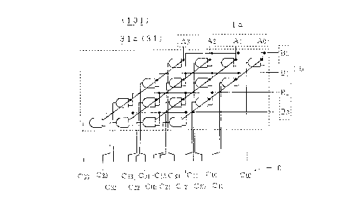
Figs. 1 and 2 are circuitry diagrams each showing a part of the structure
of a multiplier circuit 101 according to the present invention. In combination,
Figs. 1 and 2 show the entire structure of the multiplier circuit 101.
A multiplicand la (= A3 A2 Al Ao) and a multiplier lb (= B3 B2 Bl Bo)~
each expressed in binary 4 bits, are inputted to the multiplier circuit 101. Thesixth most significant bit is rounded off so that a binary S-bit multiplication
result 2 (= P7 P6 Ps P4 P3) is obtained.
The multiplier circuit 101 comprises a carry-save addition part 31.
Therefore, directly from the multiplicand la and the multiplier lb, i.e., without
using a rounding circuit which is provided external to the multiplier circuit 101,
the multiplication result 2 is obtainable by rounding off the sixth most
significant bit.
0 The addition part 31 is formed by a partial product generating part 31a
and an addition processing part 31b. The partial product generating part 31a
generates a partial product group 6 (which is formed by partial products Cjj (0
~ i, j ~ 3)) from the multiplicand la and the multiplier lb, and has the same
structure as that of the conventional partial product generating part 30a. The
partial product generating part 31a is formed by 16 (= 4 X 4) AND gates
2119283
1~
whose outputs form the partial product group 6. For example, a partial product
C30 represents a product of the most significant bit A3 of the multiplicand la
and the least significant bit Bo of the multiplier lb.
At the addition processing part 31b which receives the partial product
S group 6, an alignment of digits is carried out and stages at which an addition
is performed are matched as shown by the dotted grids. In the description
hereinafter, the addition process stages will be referred to by the number of the
stages counted from the top stage. At the first stage, half adders 7a and 7c
which are indicated at the encircled letter "h" and a rounding half adder 13
10 which is indicated at the encircled symbol "h+" are provided. At the second
stage, full adders 8a, 8b and 8c which are indicated at the encircled letter "f"
are provided. At the third stage, full adders 8d, 8e and 8f which are indicated
at the encircled letter "f" are provided. At the fourth, or the last stage, a 3-bit
carry look ahead adder 9 is provided.
At the first stage, the partial product C0O (=Ao Bo) is not processed by
any computation. The half adder 7c receives a partial product ClO (= Al Bo)
and a partial product C0l (= Ao Bl), and adds the two into a 2-bit result. The
carry digit of this output (i.e., the higher bit) is given to the full adder 8c of
the second stage. The rounding half adder 13 receives a partial product Cll (=
20 Al Bl) and a partial product C20 (= A2 Bo)~ adds these two partial products and
1, and outputs a 2-bit result. The higher bit of this output is given to the full
adder 8b of the second stage while the lower bit of the output is given to the
full adder 8c of the second stage. The half adder 7a receives a partial product
C2l (= A2 Bl) and a partial product C30 (= A3 Bo)~ The higher bit and the
25 lower bit of the total of these two partial products are given to the full adders
2119283
19
8a and 8b of the second stage, respectively.
At the second stage, the full adder 8a further receives a partial product
C2~ (= A2 B2) and a partial product C3l (= A3 Bl), the full adder 8b further
receives a partial product Cl2 (= Al B2) and the full adder 8c further receives
5 a partial product C02 (= Ao B2). Receiving the partial products, the respective
full adders perform addition of the three inputs. In a similar manner, at the
third stage, the full adder 8d, receiving a partial product C23 (= A2 B3) and a
partial product C32 (= A3 B2) and the higher bit of the full adder 8a, outputs a
2-bit value. Receiving a partial product Cl3 (= Al B3), the lower bit of the
10 output of the full adder 8a and the higher bit of the output of the full adder 8b,
the full adder 8e outputs a 2-bit value. Receiving a partial product C03 (= Ao
B3), the lower bit of the output of the full adder 8b and the higher bit of the
output of the full adder 8c, the full adder 8f outputs a 2-bit value.
At the fourth stage, to the 3-bit carry look ahead adder 9, a partial
product C33 (= A3 B3) and the higher bit of the output of the full adder 8d are
given as aligned to each other at one digit, the lower bit of the output of the
full adder 8d and the higher bit of the output of the full adder 8e are given as
aligned to each other at one digit, and the lower bit of the output of the full
adder 8e and the higher bit of the output of the full adder 8f are given as
aligned to each other at one digit.
The lower bit of the output of the full adder 8f directly becomes the least
significant bit P3 of the multiplication result 2. The remaining higher bits (P7
P6 P5 P.~) of the multiplication result 2 are outputted from the 3-bit carry look
ahead adder 9.
The rounding half adder 13 is located at a position where the sixth most
2119283
significant bit is to be calculated, i.e., a position where the half adder 7b is to
be disposed in the conventional addition processing part 30b which is shown in
Fig. This allows that an auxiliary number "1" is added to the sixth most
significant bit. Hence, as explained in "(A-0) Basic Idea," the multiplication
S result 2 which was rounded off at the sixth most significant bit and which
therefore includes the most to the fifth most significant bits is available from
the multiplier circuit 101. Since the carry-save method is used in the first
preferred embodiment, the carry-over propagation path is short, whereby a
high-speed operation is enabled.
Fig. 3 is a circuitry diagram showing a structure of each half adder,
typically the half adder 7a, of the addition processing part 31b. Fig. 4 is a
circuitry diagram showing a structure of the rounding half adder 13. In Figs.
3 and 4, inputs K and L correspond to the partial products which are shown in
Fig. 2. Outputs C and S correspond to the higher bit and the lower bit of the
1~ output of the half adder 7a or the rounding half adder 13, respectively. The
output C also corresponds to the carry digit. In the half adder 7a, an AND
gate 14 and an EXOR gate 15 are each provided with the inputs K and L. The
AND gate 14 outputs the output C and the EXOR gate 15 outputs the output
S. Thus, the sum of "K" and "L" each consisting of one bit is obtained as a
0 -bit value "CS."
On the other hand, at the rounding half adder 13, an OR gate 16 and an
EXNOR gate 17 are each provided with the inputs K and L, and the OR gate
16 outputs the output C and the EXNOR gate 17 outputs the output S. Here,
the sum of "K," "L" and the auxiliary number "1" is calculated as a 2-bit value
2~ "CS."
211928~
Fig. 5 is a circuitry diagram showing in detail a structure of the AND
gate 14 of the half adder 7a and Fig. 6 is a circuitry diagram showing in detaila structure of the OR gate 16 of the rounding half adder 13. As can be
understood by comparing Fig. 5 with Fig. 6, the gates 14 and 16 each equally
S require six transistors. Fig. 7 is a circuitry diagram showing in detail a
structure of the EXOR gate 15 of the half adder 7a and Fig. 8 is a circuitry
diagram showing in detail a structure of the EXNOR gate 17 of the rounding
half adder 13. As is evident from comparison between Figs. 7 and 8, the gates
15 and 17 each equally require ten transistors. Considering this in light of thestructures shown in Figs. 3 and 4, it can be understood that the circuit sizes of
the half adders 7a and 13 are the same. Hence, the addition processing part
31b ofthe multiplier circuit 101 is realized in the same circuit size as that ofthe conventional addition processing part 30b.
On the other hand, since the rounding circuit 5 is not necessary for the
multiplier circuit 101, the multiplier circuit 101 is formed in a smaller size t han
the conventional multiplier circuit 100. The reduction in the circuit size is
advantageous as it is, and further advantageous in that high-speed operation is
possible.
(A-2) Second Preferred Embodiment:
0 A second preferred embodiment is an application of the present invention
to a multiplication using the Wallace Tree. Fig. 9 is a circuitry diagram
showing a structure of an addition processing part 31c. The addition processing
part 31c and the partial product generating part 31a which is shown in Fig. 1
form a multiplier part 32. At the multiplier part 32, a Wallace-Tree multiplier
is formed.
2119283
That is, in the addition processing part 31c to which the partial product
group 6 is to be inputted, a half adder 7a, full adders 8a, 8b and 8c and a half
adder 7b are disposed in this order at the first stage. At the second stage, half
adders 7c, 7d and 7e, a full adder 8d and a rounding half adder 13 are disposed
S in this order. At the third stage, an OR gate 9b and a 4-bit carry look ahead
adder 9a are disposed in this order.
First, at the first stage, a partial product C00 is not processed by any
computation. The half adder 7a receives partial products C23 and C32, the full
adder 8a receives partial products C13, C22 and C3l, the full adder 8b receives
partial products C12, C21 and C307 the full adder 8c receives partial products C02,
C11 and C20, the half adder 7b receives partial products C01 and C10. Each of
the half and the full adders calculates the sum of the inputted partial products
as a 2-bit value.
At the second stage, the half adder 7c receives a partial product C33 and
15 the higher bit of the output of the half adder 7a while the half adder 7d
receives the lower bit of the output of the half adder 7a and the higher bit of
the output of the full adder 8a. The half adder 7e receives the lower bit of the
output of the full adder 8a and the higher bit of the output of the full adder 8b.
The full adder 8d receives a partial product Co37 the lower bit of the output of
0 the full adder 8b and the higher bit of the output of the full adder 8c. The
rounding half adder 13 receives the lower bit of the output of the full adder 8c
and the higher bit of the output of the half adder 7b. Each of the half and the
full adders calculates the sum of the inputted partial products as a 2-bit value.
At the third stage, to the 4-bit carry look ahead adder 9a, the lower bit
25 of the outPut of the half adder 7c and the higher bit of the output of the half
2119283
23
adder 7d are given as aligned to each other at one digit, the lower bit of the
output of the half adder 7d and the higher bit of the output of the half adder
7e are given as aligned to each other at one digit, the lower bit of the output
of the half adder 7e and the higher bit of the output of the full adder 8d are
5 given as aligned to each other at one digit, and the lower bit of the output of
the full adder 8d and the higher bit of the output of the rounding half adder 13
are given as aligned to each other at one digit. The OR gate 9b calculates a
logical sum of a carry output (the most significant bit) of the carry look ahead
adder 9a and the higher bit of the output of the half adder 7c so that the most
10 significant bit P7 of the multiplication result 2 is outputted. The carry look
ahead adder 9a outputs the remaining higher bits (P6 P5 P4 P3) of the
multiplication result 2.
Since the rounding half adder 13 is located at a position where the sixth
most significant bit is to be calculated, an auxiliary number is added to the
1~ sixth most significant bit. Hence, the effect of the present invention is also
assured where a multiplication using the Wallace Tree is to be performed. In
other words, it is possible to obtain the multiplication result 2 which was
rounded off at the sixth most significant bit without using an externally provided
rounding circuit. More advantageously, the addition processing part 31c requires
0 only a reduced number of the stages as compared with the addition processing
part 31b of the first preferred embodiment.
(A-3) Third Preferred Embodiment:
A third preferred embodiment is an application of the present invention
to a multiplication using the Booth algorithm. Fig. 10 is a circuitry diagram
2~ showin~ a stnlcture of a multiplier circuit 102 according to the present
2119283
24
invention. The multiplier circuit 102 is supplied with an 8-bit multiplicand
X7-Xo and an 8-bit multiplier Y7-Yo which are negative numbers each
expressed as a complement of 2. Without using an externally provided rounding
circuit, a binary 12-bit multiplication result 21 (= Pls .. Ps P4) rounded off at
5 the thirteenth most significant bit is obtained.
The multiplier circuit 102 comprises a multiplier part 33 adopting the
Booth algorithm. The multiplier part 33 is formed by a partial product
generating part 33a and an addition processing part 33b.
The product generating part 33a generates four partial products from the
10 multiplicand X7-Xo and the multiplier Y7-Yo The product generating part 33a
comprises four types of Booth partial product generating circuits 331 to 334.
The Booth partial product generating circuit 331 generates a 16-bit partial
product from the multiplicand X7-Xo and the least two significant bits Yl Y0 of
the multiplier. The Booth partial product generating circuit 332 generates a
1~ 14-bit partial product from the multiplicand X7-Xo and the fifth, sixth and
seventh most significant bits Y3 Y2 Yl of the multiplier. The Booth partial
product generating circuit 333 generates a 12-bit partial product from the
multiplicand X7-Xo and the third, fourth and fifth most significant bits Ys Y4
Y3 of the multiplier. The Booth partial product generating circuit 334 generates
0 a 10-bit partial product from the multiplicand X7-Xo and the first, second and
third most significant bits Y7 Y6 Ys of the multiplier.
These four types of partial products are inputted to the addition processing
part 33b with their most significant bits aligned to each other. For clarity of
illustration, Fig. 10 shows only the bits in the vicinity of the most and the least
25 significant bits as being inputted to the addition processing part 33b.
2119283
2~
The addition processing part 33b is formed as a four-stage part. At the
first stage, half adders 7a to 71, a rounding half adder 13 and a half adder 7m
are disposed in this order from the higher bit side. At the second stage, full
adders 8a to 81 and a half adder 7n are disposed in this order from the higher
S bit side. At the third stage, full adders 8m to 8v and half adders 7O and 7p
are disposed in this order from the higher bit side. At the fourth, or the last
stage, an 11-bit adder 91 is disposed.
Fig. 11 is a circuitry diagram showing the structure of the addition
processing part 33b in more detail than in Fig. 10. At the first stage, each bit
10 of the output of the Booth partial product generating circuit 331 is given in a
decreasing order from the most significant to the fourteenth bits to each one of
the half adders 7a to 71, the rounding half adder 13 and the half adder 7m. In
addition, each bit of the output of the Booth partial product generating circuit
332 is given in a decreasing order from the most significant to each one of
15 these adders.
Next, at the second stage, the full adder 8a receives the output of the half
adder 7a, the higher bit of the output of the half adder 7b and the most
significant bit of the output of the Booth partial product generating circuit 333;
the full adder 8b receives the lower bit of the output of the half adder 7b, the
20 higher bit of the output of the half adder 7c and the second significant bit of
the output of the Booth partial product generating circuit 333; the full adder 8c
receives the lower bit of the output of the half adder 7c, the higher bit of the
output of the half adder 7d and the third significant bit of the output of the
Booth partial product generating circuit 333; the full adder 8d receives the lower
2~ bit of the output of the half adder 7d, the higher bit of the output of the half
2119283
26
adder 7e and the fourth significant bit of the output of the Booth partial product
generating circuit 333; the full adder 8e receives the lower bit of the output of
the half adder 7e, the higher bit of the output of the half adder 7f and the fifth
significant bit of the output of the Booth partial product generating circuit 333;
S the full adder 8f receives the lower bit of the output of the half adder 7f, the
higher bit of the output of the half adder 7g and the sixth significant bit of the
output of the Booth partial product generating circuit 333; the full adder 8g
receives the lower bit of the output of the half adder 7g, the higher bit of the
output of the half adder 7h and the seventh significant bit of the output of the
10 Booth partial product generating circuit 333; the full adder 8h receives the lower
bit of the output of the half adder 7h, the higher bit of the output of the half
adder 7i and the eighth significant bit of the output of the Booth partial product
generating circuit 333; the full adder 8i receives the lower bit of the output of
the half adder 7i, the higher bit of the output of the half adder 7j and the ninth
15 significant bit of the output of the Booth partial product generating circuit 333;
the full adder 8j receives the lower bit of the output of the half adder 7j, the
higher bit of the output of the half adder 7k and the tenth significant bit of the
output of the Booth partial product generating circuit 333; the full adder 8k
receives the lower bit of the output of the half adder 7k, the higher bit of the
20 output of the half adder 71 and the eleventh significant bit of the output of the
Booth partial product generating circuit 333; and the full adder 81 receives the
lower bit of the output of the half adder 71, the higher bit of the output of the
rounding half adder 13 and the twelfth signif1cant bit of the output of the Booth
partial product generating circuit 333. The half adder 7n receives the lower bit
25 of the output of the rounding half adder 13 and the higher bit of the output of
2119283
the half adder 7m.
Following this, at the third stage, the full adder 8m receives the output
of the half adder 8a, the higher bit of the output of the half adder 8b and the
most significant bit of the output of the Booth partial product generating circuit
334; the full adder 8n receives the lower bit of the output of the half adder 8b,
the higher bit of the output of the half adder 8c and the second significant bit
of the output of the Booth partial product generating circuit 334; the full adder
80 receives the lower bit of the output of the half adder 8c, the higher bit of
the output of the half adder 8d and the third significant bit of the output of the
10 Booth partial product generating circuit 334; the full adder 8p receives the lower
bit of the output of the half adder 8d, the higher bit of the output of the half
adder 8e and the fourth significant bit of the output of the Booth partial product
generating circuit 334; the full adder 8q receives the lower bit of the output of
the half adder 8e, the higher bit of the output of the half adder 8f and the fifth
15 significant bit of the output of the Booth partial product generating circuit 334;
the full adder 8r receives the lower bit of the output of the half adder 8f, the
higher bit of the output of the half adder 8g and the sixth signifcant bit of the
output of the Booth partial product generating circuit 334; the full adder 8s
receives the lower bit of the output of the half adder 8g, the higher bit of the
0 output of the half adder 8h and the seventh significant bit of the output of the
Booth partial product generating circuit 334; the full adder 8t receives the lower
bit of the output of the half adder 8h, the higher bit of the output of the half
adder 8i and the eighth significant bit of the output of the Booth partial product
generating circuit 334; the full adder 8u receives the lower bit of the output of
2~ the half adder 8i, the higher bit of the output of the half adder 8j and the ninth
2119283
28
significant bit of the output of the Booth partial product generating circuit 334;
and the full adder 8v receives the lower bit of the output of the half adder 8j,
the higher bit of the output of the half adder 8k and the tenth significant bit of
the output of the Booth partial product generating circuit 334. The half adder
5 70 receives the lower bit of the output of the full adder 8k and the higher bit
of the output of the full adder 81 while the half adder 7p receives the lower bit
of the output of the half adder 81 and the higher bit of the output of the half
adder 7n.
At the fourth stage, to the 11-bit adder 91, the output of the full adder
10 8m and the higher bit of the output of the full adder 8n are given as aligned
to each other at one digit, the lower bit of.the output of the full adder 8n and
the higher bit of the output of the full adder 80 are given as aligned to each
other at one digit, the lower bit of the output of the full adder 80 and the
higher bit of the output of the full adder 8p are given as aligned to each other
15 at one digit, the lower bit of the output of the full adder 8p and the higher bit
of the output of the full adder 8q are given as aligned to each other at one
digit, the lower bit of the output of the full adder 8q and the higher bit of the
output of the full adder 8r are given as aligned to each other at one digit, the
lower bit of the output of the full adder 8r and the higher bit of the output of
. 0 the full adder 8s are given as aligned to each other at one digit, the lower bit
of the output of the full adder 8s and the higher bit of the output of the full
adder 8t are given as aligned to each other at one digit, the lower bit of the
output of the full adder 8t and the higher bit of the output of the full adder 8u
are given as aligned to each other at one digit, the lower bit of the output of
25 the full adder 8u and the higher bit of the output of the full adder 8v are given
2119283
29
as aligned to each other at one digit, the lower bit of the output of the full
adder 8v and the higher bit of the output of the half adder 7O are given as
aligned to each other at one digit, and the lower bit of the output of the half
adder 7O and the higher bit of the output of the half adder 7p are given as
5 aligned to each other at one digit. As a result, the output of the adder 91
becomes the higher bits of the multiplication result 21 (Pls to Ps)~ The least
significant bit P4 of the multiplication result 21 is the lower bit of the output
of the half adder 7p.
Since the rounding half adder 13 is located at a position where the
10 thirteenth most significant bit is to be calculated, an auxiliary number is added
to the thirteenth most significant bit. Hence, the effect of the present invention
is also assured where a multiplication using the Booth algorithm is to be
performed. In other words, it is possible to obtain the multiplication result 21
which was rounded at the thirteenth most significant bit without using an
15 externally provided rounding circuit.
The rounding half adder 13 is located at a position where the thirteenth
most significant bit is to be calculated as described above. It then follows that
the rounding half adder 13 may be disposed at other stages, not necessarily at
the first stage as in the case of the addition processing part 33b. Fig. 12 is a
20 circuitry diagram of a addition processing part 33c which is equal in structure
to the addition processing part 33b as it is modified so that the half adder 7n
and the rounding half adder 13 are replaced with each other.
When the addition processing part 33c having such a structure is used in
combination with the product generating part 33a, the present invention is
25 applicable to a multiplication using the Booth algorithm.
2119283
B. Divider Circuit:
(B-0) Basic Idea:
A basic idea of the present invention will be described before discussing
the details of the present invention. Assume an example where an 8-bit
S dividend A (= A7 A6 ... Ao) is divided by an 8-bit divisor B (= B7 B6 ... Bo >
A) to obtain a rounded quotient which is smaller than 1. To obtain a division
result which is rounded off to the eight decimal places, A B is to be
calculated and 2-9 is to be added to the quotient. The wanted quotient which
is rounded off to the eighth digit down from the radix point is obtained as a
10 result. In short, Q = A B + 2-9 iS to be calculated to the eight decimal
places.
The equation above can be modified as Q = (A + B x 2-9) ~ B.
Hence, a desired calculation result is obtainable by dividing a newly adopted
dividend (A + B Y' 2-9) by the divisor B to the eight decimal places.
Especially in this case, while the least significant bit has a weight (digit)
of 2~, the most significant bit of B x 2-9 has a weight of 2-2. Therefore, a
calculation result yielded from the new dividend (A + B Y 2-9) is 17-bit data
(A7 A6 Ao 0 B7 B6 Bl Bo) which should be divided by B to the digit of
2-8 (i.e., to the eighth digit down from the radix point). To this end, of the
20 17-bit data, the higher sixteen bits are needed, which implies that it is necessary
to divide (A7 A6 ... Ao 0 B7 B6 ... Bl) by (B7 B6 ... Bo) Hence, there is no
need to newly provide the rounding circuit 5 as in the conventional technique
or to calculate a quotient to the ninth digit down from the radix point, allowing
omission of one stage from the structure of the quotient determining circuit.
(B-1) Fourth Preferred Embodiment:
2119~83
31
Fig. 13 is a circuitry diagram showing a structure of a division circuit
201 according to the present invention. The division circuit 201 is constructed
to divide an 8-bit dividend A by an 8-bit divisor B (> A) and to round off the
ninth digit down from the radix point to thereby obtain a quotient to the eighth
5 digit down from the radix point. For this purpose, the division circuit 201
comprises 1-bit quotient determining parts 12a to 12h.
First, the 8-bit dividend A and the 8-bit divisor B are given to the 1-bit
quotient determining part 12a. Since a relation A < B is satisfied, the value
over the radix point is always 0. Hence, the value "0" is also given to the
10 1-bit quotient determining part 12a.
At the 1-bit quotient determining part 12a, the value "0" is added to the
end of the 8-bit dividend A so that 9-bit data (A7 A6 ... AD 0) is generated.
This data corresponds to the nine most significant bits of the new 17-bit
dividend which has been explained in "(B-0) Basic Idea." Since a quotient for
only one bit has to be determined at the 1-bit quotient determining part 12a,
there is no need to calculate all digits of the new 17-bit dividend and to divide
the 17-bit dividend by the divisor B. Rather, it is necessary only to add the
1-bit value "0" to the end of the 8-bit dividend A. In this manner, the
quotient q7 for the most significant digit and the 8-bit remainder R8 are
calculated at the 1-bit quotient determining part 12a. Fig. 14 is an explanatory
diagram showing the calculation at the 1-bit quotient determining part 12a in
the form of a calculation with figures.
Next, the 8-bit remainder R8 and the 8-bit divisor B are given to the
1-bit quotient determining part 12b. Further, in sharp contrast from the
conventional technique, not only the value "0" but also the most significant
2119283
32
value B7 of the divisor B, which corresponds to the tenth most significant bit
of the new dividend, are given to the 1-bit quotient determining part 12b. At
the 1-bit quotient determining part 1 b, the value B7 is added to the end of the
8-bit remainder R8 to generate 9-bit data which will be then divided by the
5 divisor B. Fig. 15 is an explanatory diagram showing the calculation at the
1-bit quotient determining part 12b in the form of a calculation with figures.
As shown in Fig. 15, to add the value B7 to the end of the 8-bit remainder R8
and to thereafter divide the resultant value by the divisor B are, as far as
determination of a 1-bit quotient for the second digit down from the radix point
10 is concerned, equivalent to a division of the new 17-bit dividend by the devisor
B. In this manner, the 1-bit quotient q6 for the second digit down from the
radix point and the 8-bit remainder R7 are calculated at the 1-bit quotient
determining part 12b.
In a similar manner, the 1-bit quotient determining parts 12c to 12h are
15 respectively provided with remainders R7 to R2 which are calculated at the
respective preceding 1-bit quotient determining parts 12b to 12g. As the divisor
B is given, 1-bit values B6 to Bl which form the divisor B are also given to
the 1-bit quotient determining parts 12c to 12h, and are respectively added to
the ends of the remainders R7 to R2. The 1-bit quotient determining parts 12c
20 to 12h output 1-bit quotients q5 to qO, respectively.
Thus, by adding a 1-bit value which forms the divisor to the end of the
dividend at each 1-bit quotient determining part, division of the new 17-bit
dividend by the divisor B is substantially performed. Hence, as described in
"(B-0) Basic Idea," it is possible to round off the ninth digit down from the
25 radix point to thereby obtain a quotient which has eighth digit down from the
2119283
33
radix point.
It is to be noted in a case where a quotient is to be calculated down to
seventh digit from the radix point by dividing an 8-bit dividend A by an 8-bit
divisor B (> A) and by thereafter rounding off the eighth digit, the new dividend
S is a 16-bit value (A7 A6 .. Ao B7 B6 .. B), the 1-bit quotient determining part
12a is not necessary. Fig. 16 is a circuitry diagram showing a structure of a
division circuit 201a which is to be used where such a calculation is to be
performed. To the 1-bit quotient determining part 12b, the dividend A is given
instead of the remainder R8. At the 1-bit quotient determining part 12b, the
10 value B7 is added to the end of the dividend A. Calculations to follow are the
same as those performed in the division circuit 201.
To calculate a quotient down to ninth digit from the radix point by
dividing an 8-bit dividend A by an 8-bit divisor B (> A) and by thereafter
rounding off the tenth place, an 18-bit value (A7 A6 ... Ao 0 0 B7 B6 ... B) has
15 to be used as the new dividend. Hence, in this case, a new 1-bit quotient
determining part 12x needs be provided. Fig. 17 is a circuitry diagram showing
a structure of a division circuit 201b which is to be used where such a
calculation is to be performed. The 1-bit quotient determining part 12x receives
the dividend A, the divisor B and a 1-digit value "0," and divides the 9-bit
number (A7 A6 .. Ao 0) by the divisor B, whereby a 1-bit quotient q8 and an
8-bit remainder R9 are yielded. Next, at the 1-bit quotient determining part
12a, a 1-digit value "0" is added to the end of the remainder Rg. Calculations
to follow are the same as those performed in the division circuit 201.
Unlike the conventional division circuit, the division circuits 201, 201a
2~ and 201b do not need the rounding circuit 5. In addition, these division circuits
2119~83
34
comprise one stage less of 1-bit quotient determining circuits. Moreover, the
1-bit quotient determining circuits used in these division circuits are the same
in structure as those used in the conventional division circuit, and therefore the
circuit size for one stage is approximately the same as that in the conventional
5 division circuit. Hence, a smaller circuit size and a quicker operation are
possible in these division circuits than in the conventional division circuit.
(B-2) Fifth Preferred Embodiment:
In the present invention, if the digit of the rounding-off position is
located at an L-th digit down from the radix point, depending on a relation
10 between the number of digits of a dividend M and the number L, the division
circuit can have different structures. The fourth preferred embodiment
corresponds to where there is a relation L 2 M, and therefore, "the new
dividend" is calculated in a relatively simple manner. However, if the relation
between L and M is L < M, in some cases, it is necessary to dispose an adder
15 prior to the 1-bit quotient determining circuits. The fifth preferred embodiment
deals with such a case.
Fig. 18 is a circuitry diagram showing a structure of a division circuit
O 2 according to the present invention. The division circuit 202 is a circuit for
dividing an 8-bit dividend A by an 8-bit divisor B (> A) and by thereafter
0 rounding off the fifth digit down from the radix point in order to obtain a
quotient which has four digits down from the radix point. The division circuit
0 comprises 1-bit quotient determining parts 12b to 12e and an adder 19.
From the new dividend (A + B >< 2-5), 13 bits [A7, A6, As~ A4, A3,
(A2 + B7), (Al + B6), (Ao + B5), B4, B3, B2, Bl, Bo~ are obtained as a
'~ calculation result. To this end, at the adder 19, the most three significant bits
2119283
must be added to the least three significant bits of the dividend A. In other
words, the dividend A and relatively higher three digits B7, B6 and Bs which
form the divisor B are given to the adder 19.
Now, assume that in the binary system, A B < 0.11111. In this case,
S a (rounded) quotient 22 to be calculated is smaller than 1 and therefore its value
at the digit over the radix point is "0." Hence, an output R5 of the adder 19
is expressed in 8 bits. The output Rs corresponds to the eight most significant
bits of the new dividend (A + B x 2-5).
An output Rs of the adder 19 and the divisor B are given to the 1-bit
10 quotient determining part 12b. The fourth significant bit B4 of the divisor B is
also given to the 1-bit quotient determining part 12b and added to the end of
the output Rs. The 1-bit quotient determining part 12b performs a division in
a similar manner to the fourth preferred embodiment. Fig. 19 is an explanatory
diagram showing the calculation at the 1-bit quotient determining part 12b in
15 the form of a calculation with figures. As shown in Fig. 19, to add the value
B4 to the end of the output Rs and to divide the resultant value by the divisor
B are, as far as determination of a 1-bit quotient for the first significant bit
from the radix point is concerned, equivalent to a division of the new 13-bit
dividend by the devisor B. In this manner, at the 1-bit quotient determining
20 part 12b, a quotient q3 for the first significant bit from the radix point and an
8-bit remainder R4 are calculated.
Following this, similarly to the fourth preferred embodiment, 1-bit
quotients q2, ql and qO are calculated in this order. By calculating the quotient
qO which is at the fourth digit down from the radix point, the desired quotient
25 22 is obtained.
2119283
36
In the fifth preferred embodiment, similarly to the fourth preferred
embodiment, it is not necessary to calculate the new dividend as a whole at one
time. The division circuit according to this embodiment is formed only by the
same number of 1-bit quotient determining parts as the number of digits which
5 are to be calculated. While the rounding circuit 5 is not necessary, the adder
19 is needed. Thus, the circuit structure of the division circuit according to this
embodiment comprises one stage less as compared with the conventional division
circuit. This reduces the circuit size and attains a higher speed operation.
The present invention is also applicable to where A B < 0.11111 is
10 not satisfied in the binary system. In this case, the (rounded) quotient 22 to be
calculated is equal to or larger than 1, and its value at the digit over the radix
point is "1." Hence, the output Rs of the adder 19 is expressed in 9 bits. The
output Rs corresponds to the most nine significant bits of the new dividend (A
+ B >< 2-5).
Fig. 20 is a circuitry diagram showing a structure of a division circuit
203 which is adaptive to where there is a possibility such a relation as above
may exist between the dividend A and the divisor B. The division circuit 203
is equal in structure to the division circuit 202 as it is modified to newly
comprise the 1-bit quotient determining part 12a between the adder 19 and the
0 1-bit quotient determining part 12b. In the same way as the adder 19 does in
the division circuit 20, the adder 19 adds the relatively higher three bits B7,
B6 and Bs which form the divisor B to the dividend A while aligning the least
significant bit of these three bits to the least significant bit of the dividend A.
As a result, the 9-bit output R6 is given from the adder 19 to the 1-bit quotient
5 determining part 1 a.
2 11~2~3
The 1-bit quotient determining part 12a is provided with the divisor B
so that a quotient q4 for the first bit over the radix point is calculated. If A
B < 0.11111 in the binary system, the quotient q4 is 0 and otherwise 1. The
1-bit quotient determining part 12a outputs the 8-bit remainder R5 as well in
5 addition to the quotient q4.
Following this, calculations similar to those performed in the division
circuit 202 are carried out to thereby yield the quotient 22 which is rounded off
at the fifth digit down from the radix point and therefore which eventually has
four digits.
For the division circuit 203, one more of the 1-bit quotient determining
parts than the number of the decimal digits which are to be calculated needs be
provided, which structure is the same as in the conventional division circuit.
While the rounding circuit S is not necessary, the adder 19 is needed. Hence,
a large reduction in the circuit size as compared with the conventional division
1~ circuit is impossible. However, whereas it is necessary to perform calculations
down to a digit which is one digit lower than the digit to which a quotient is
to be finally calculated in the conventional technique, in the division circuit 203,
an already rounded result can be obtained serially from the most significant
digit. This is advantageous in that the desired result is obtainable, although
0 partially, from the most significant digit which has the most important
information. ~
Although the preferred embodiments heretofore described all deal with
where the values are all binary numbers, the prcsent invention is applicable not
only to a binary multiplication and a binary division. Rather, the present
25 invention is generally applicable to a multiplication and a division of any other
21192~3
38
numerical system where the radix D is an integer which is equal to or larger
than In this case, as an auxiliary number to be used in the multiplier circuit,
a minimum number which is equal to or larger than half the value D may be
used.
S While the invention has been described in detail, the foregoing description
is in all aspects illustrative and not restrictive. It is understood that numerous
other modifications and variations can be devised without departing from the
scope of the invention.