Note: Descriptions are shown in the official language in which they were submitted.
S P E C I F ~ C A T 1 Q N 2~19 29 7
TITLE
"TRANSMISSION/RECEPTION CIRCUIT
IN A PASSIVE OPTICAL TELECOMMUNICATION SYSTEM"
BACKGROUND OF THE INVENTION
Flold ot the In~ntlon
The present invention is directed to a transmission/reception circuit in a passive
optical telecommunication system of the type having a central station in communication
with a plurality of subscriber sta~ions via respective optical waveguides.
De~crlptlon ot the Prlor Art
P~ecent developments in telecommunications technology have lead to passive
optlcal tcl~communlcation systems wherein a plurality of dscentralized stations (subscriber
locatlons, or so-called distant units respectively combining a plurality of subscriber
locations) are respectively connected via their own light waveguide subscriber line to an
optical brancher. The optical brancher is connected directly or via at least one further
optlcal brancher to a common light waveguide terminal of a central station - particularly
an exchange - via a light waveguide bus. Such systems are described in European
Appllcatlon 0 171 080; "Passive Flbre Local Loop for Telephone with Broadband
Upgrade," Oakley et al., ISSLS' 88, Conf. Papers pp. 9.4.1-9.4.5; and "The Provision of
Telephony over Passive Optlcal networks," Hoppitt et al., BR Telecom Technol. J. Vol. 17
(1989) pp 100-113).
In such a passive optical telecommunication system, when the electro-optical
transducers of the central equipment (exchange) and of the decentralized equipment
(subscriber locatJons or distant units) preferably established by laser diodes transmit
optlcal digital signals in the baseband with the same wavelength, i.e, in common-
frequency operation, the optical signals emitted by each location in such a
--1--
by a PlN-diode) due to reflections in the optical fiber network (optical cross talk), and thus
can noticeably reduce the reception sensitivity thereof. Particularly critical is the
approximately 1 through 10% reflectivity of laser diodes conventionally provided in
decentralized equipment as electro-optical transducers. This is because measures for
reducing reflection at laser diodes lead to a poorer coupling of the laser to the optical
fiber, and thus to a lower optical power in the optical fiber, but parts of the light emitted
by the central station are simultaneously reflected proceeding from all decentralized
equipment to the opto-electrical transducer of the central station.
One can attempt to compensate for this problem by reducing the number of
decentralized stations (subscriber stations or distant units) per light waveguide terminal
of the central station (exchange), and thus the demands made of the reception sensitivity
of the central equipment are correspondingly reduced. This, however, means an increase
In the number of light waveguide terminals in the central station and thus makes the entire
system substantially more expensive, as would likewise the theoretically possible
employment of optical isolators.
SUMMARY OF THiE INVENTION
An obJect of the present invention is to provide a solution to the problem of
reflectlon at decentralized laser diodes outlined above without significantly increasing the
cost and/or complexity of the system.
The Invention is directed to a transmission/reception circuit, preferably for use in
a decentralized station Tn ~ passive optical telecommunication system wherein a plurality
of decentralized station, particularly subscriber locations or distant units combining a
plurality of subscriber locations, are respectively connected via their own light waveguide
subscriber line to an optical brancher, that is in turn connected directly or via at least one
further optical brancher to a common light waveguide terminal of the central station,
particularly an exchange, via a light waveguide bus. The decentralized station and the
--2--
-
21~9~97
central station each transmit and receive optical digital signals in common-frequency
operation. The transmission/reception circuit, in accordance with the principles of the
present invention, has an opto-electrical reception transmission transducer with an output
connected to the input s: f an electro-optical transducer via an electrical reception signal
inverter, and further has an optical delay line having a delay time matched to the
operating time (i.e., the time required for the inversion) of the elactrical reception signal
inverter. The delay line is inserted between the output of the electro-optical transmission
transducer and the light waveguide subscriber line, or between an optical directional
coupler that connects the subscriber to the input of the opto-electrical reception
trsnsducer and the output of the electro-optical transmission transducer.
The invention, which makes use of the fact that the reception sensitivity of an opto-
electrlcal transducer is especially degraded given a fluctuating intensity of the received
llght whereas a constant light level given an appropriate receiver design, has only a slight
Infiuence on the reception sensitivity. The invention produces the advantage of each
transmitting location avoiding an overdrive of its own opto-electrical transducer produced
by renected transmission light signal parts in the bit pattern of the transmission signal
(particulariy at the central station) and of avoiding a degradation of the reception
sensltivlty for subsequent reception light signals that are associated therewith, and which
correspond to the bit pattern of the transmission signal.
DESCRIPTION OF THE DRAWIN~S
Further characteristics of the invention may be seen from the following description
with reference to the drawing wherein a bi-directional light waveguide telecommunication
system havlng a plurality of transmission/reception circuits of the invention is
schematically shown.
r . ., ~
. .
2 ~ 7
DESCRIPTION OF THE PREFERRED EMBODlMENT:i
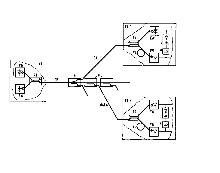
In the bi-directional light waveguide t01ecommunication system outlined in the
drawing, a passive (preferably monomode) light waveguide bus network extends between
a central telecommunication station VSt which, for example, can be an exchange - anrl
a plurality of decentralized t01ecommunication stations TSt1,...,TS~n. Such decentralized
telecommunication stations can be subscriber locations, or so-called distant units which
respectively combine a plurality of subscriber locations. Each station (central and
decentralized) includes interface equipment provided with an electro-optical transmlssion
transducer SW and an opto-electrical reception transducer EW which, possibly with the
assistance of a multiplexer or demultiplexer (not shown in detail in tha drawing) Iying at
the electrical side of the transmission or reception transducer, are capable of combining
or spllttlng up to 32 ISDN-B channels.
In this light waveguide telecommunication system, the decentralized stations TSt
are connected by a single-fiber light waveguide bus OB to a common light waveguide
muitiplex terminal of the central telecommunication station VSt. The light waveguide
subscriber lines OAL1,...,0ALn belonging to the individual decentralized stations
TSt1,...,TStn may be assumed to be connected to the appropriate light waveguide bus
OB via passive optical branchers V accommodated, for example, in cable branchsr
houslngs. This connection can be made directly or via further such branch~rs. Tandem
mlxers or optical directional couplers, for example, can be employed as optical branchers.
As Indicated in the drawing, it is also possible - as is known, for example, from European
Appllcation 0 171 080 - to provide common optical branchers shared by a plurality of light
waveguide subscriber lines (OAL).
In the telecommunication system outlined in the drawing, the individual
telecommunication stations TSt1 ,...,TStn and VSt are each provided with an opto-electrical
reception transducer EW having a PIN diode and with an electro-optical transmission
transducer SW having a laser diode. For decoupling electro-opti~l transmission
--4--
transducers SW and opto-electrical reception transducers EW and for separating
directions as well, an optical directional coupler (2x2 coupler) RK is inserted between the
light waveguide subscriber line OAL (or at the central station, the bus OB) and both the
opto-electrical reception transducer i~W and electro-optical transmission transducer SW
for that station. The telecommunication stations TSt1 ,...TStn and VSt transmit and receive
optical digital signals in common-frequency operation.
In order to then prevent parts of digital optical signals, transmitted (in a bit pattern)
by the central station VSt and reflected (in a proportionally reduced amplitude bit pattern)
by the laser diodes of the electro-optical transducers SW contained in the decentralized
stations TSt1,...TStn, degrading the sensitivity of the opto-electrical transducer EW of the
central station VSt, the decentralized telecommunication stations TSt1,...,TStn are each
provided with transmission/reception circuits of the invention. As the drawing shows, the
output of the opto-electrical transducer EW at each station is connected to the input of
the electro-optical transducer SW at that station via an electrical reception signal invertor
J. Also, an optical delay line VL whose delay time is matched to the operating time of the
electrical reception signai invertor J is inserted between the output of the electro-optical
transducer SW and the optlcal directional coupler connecting that output to the light
wave~uide subscriber line OAL - or connecting the latter to the input of the opto-electrical
transducer EW. An approximately 10 through 100 cm long optical fiber is thereby
required for a delay time of approximately 0.5 through 5 ns.
The bl-directional light waveguide telecommunication system outlined in the
drawlng th~n basically operates in the following way. When an optical signal component
exhibitlng maximum optical power (i.e., a "1") is transmitted by the central
telecommunlcation station VSt, this proceeds via the light waveguide bus OB and the
passive optical branchers V to the individual decentralized telecommunication stations
TSt1 ,...,TStn, and proceeds at each station via the respactive optional directional coupler
RK to the reception transducer EW and to the transmission transducer SW. A part of the
--5--
- : ~ . : :
2~2~7
optical power is unavoidably reflected at the laser diod0 of the transmission transducer
SW. The received electrical signal component (i.e., a ~ ) appearing at the output of the
reception transducer EW also drives the electrical reception signal invertor J so that a low
signal component (i.e., a "0") appears at the output thereof, this low signal component in
turn proceeds to the input of the transmission transducer SW, but it effects no additional
modulation of the laser diode at the transducer SW.
When an optical signal element characterized by minimum optical power (i.e., a "0")
is transmitted from the central telecommunication station VSt, this again proceeds via the
light waveguide bus OB and the passive optical branchers V to the individual
decentralized telecommunication stations TSt1,...TStn, and proceeds at each station via
its optical directional coupler RK to the reception transducer EW and to the transmission
transducer SW. Again, a part of the optical power is unavoidably reflected at the laser
dlode of the transmission transducer SW. The electrical signal component "0" now
appearing at the output of the reception transducer EW also drives ths electrical reception
signal invertor J, so that a signal component "1" now appears at the output thereofj which
in turn proceeds to the input of the transmission transducer SW. This signal component
~'1 n then effects an additlonal modulation of the laser diode of the transmission transducer
SW. Thls additional modula~ion is superimposed on (added to) that part of the optical
slgnal component "0" Just arriving after traversing the optical delay llne VL and reflected
by it, thereby causing the transducer SW to deliver an o~tput exactly at a light power that
is equal to the light power that was previously delivered upon the arrival of an optical
slgnal component "1". The output Is the same independently of whether optical signal
components of "0" or "1" were received, because the sum of the light power reflected
because of received optical signal elements and potentially additionally transmitted
(reflected) is held at a constant level. The result in the centralized telecommunication
station VSt is that the reception light level is likewise independent of the bit pattern of its
own transmitted optical signal. Thus a dagradation of tha raception sensitivity of the opto-
--6--
2~ ~2.~7
electrical transducer EW of the central telecommunication station VSt corresponding tothe bit pattern o~ the transmission optical signal is avoided.
The electrical reception signal invertor J, which as indicated in the drawing, can be
formed by an inverting amplifier, can be capacitively connected to a following current
source circuit A for additional modulation of the laser diode of the transmission transducer
SW, so that a control current i output by the current source circuit A corresponds to the
average received optical power. This has the consequence that, given an increase in or
reduction of the optical power received in the decentralized station TSt which may occur,
for example, due to a long-term drift of the laser diode SW active in the central station TSt
or also due to changes in the configuration of the light waveguide telecommunication
system which may slightly vary the high ("1") level, the additional modulation of its laser
diode 18 correspondingly increased or reduced. The sum of the light power reflected due
to recelved optlcal signal elements and potentially additionally transmitted (reflected) is
thus kept at a constant level even given varyin0 optical reception power.
Aithough modifications and changes may be suggested by those skilled in the art,
it is the intention of the inventor to embody within the patent warranted hereon all
changes and modifications as reasonably and properly come within the scopz of his
contrlbutlon to the art.
--7--
. ! , .
.: '' ~ ' ' . ~