Note: Descriptions are shown in the official language in which they were submitted.
CA 02119438 2001-03-27
1
THREE WIRE LOW POWER TRANSMITTER
BACKGROUND OF THE INVENTION
This invention relates to process variable transmitters
receiving power over two of three wires and communicating over
a third wire to a controller.
SUMMAIR'Y OF THE INVENTION
In a first aspect, the invention provides a three wire
transmitter bidirectionally communicating AC signals to and
from a first device external to the transmitter, and sending
DC signals thereto, the three wire transmitter comprising a
power terminal and a common terminal connected to
corresponding power and common terminals of an energization
source external to the transmitter, and sensing means,
energized from the power terminal and the common terminal, for
providing a sensor output: indicative of a process variable
(PV) sensed by the sensing means.
The three wire transmitter also comprises communication
means energized from the power terminal and the common
terminal, including means; for storing transmitter data for the
transmitter, the communication means receiving the sensor
output for providing a Df. signal and a first AC signal to a
signal terminal connected to the first external device, and
receiving a second AC signal from the first external device,
the DC signal representative of the sensed PV and the first AC
signal representative of the sensed PV and of transmitter data
selected by the second AC signal, the communication means
having a characteristic A.C impedance between the signal
terminal and the common terminal for receiving and
transmitting the first and second AC signals to and from the
first external device so that the second AC signal is of a
CA 02119438 2001-03-27
la
sufficiently large amplitude and so that the first AC signal
is received, the communication means having a characteristic
DC impedance substantially lower than the DC impedance of the
first external device for transmitting the DC signal.
In a second aspects, the invention provides a three wire
transmitter bidirectiona.l.ly communicates AC signals to and
from a first external device and sends DC signals to a second
external device. The transmitter has power and common
terminals which connect t.o corresponding power and common
10~ terminals of an external energization source. The transmitter
includes sensing means which are energized from the power and
common terminals, for providing a sensor output indicative of
a process variable (PV) sensed by the sensing means. Also
included are communication means energized from the power and
common terminals, including memory storage for transmitter
status and PV. The communication means receives the sensor
output and provides the DC signal and the AC signal to a
signal terminal which connects to both external devices, and
also receives AC signals fz:om the first external device. The
20 DC signal is representative of the sensed PV, over a range of
frequencies which include DC, and the AC signal is digitally
representative of the sensed PV and of transmitter data
selected by the received AC signal. The communication means
have a characteristic AC impedance between the signal and
common terminals over an AC frequency range for receiving and
transmitting AC signals to and from the first external device
so that the receiving si~~nals are not shorted out and so the
transmitted signals can be received. The communication means
have a characteristic DC impedance between the
WO 93/06576 ~ ~ .~, 01 ~~~ r~ :.i PCT/US92/0703$
-2-
signal and common terminal over a range. of frequencies
which include DC and typically extends to about 20Hz.
The DC characteristic impedance is substantially lower
than the impedance of the second external device which
receives DC signals so that the accuracy of the
transmitted DC signal is not compromised. In one
application, the functions of the first and the second
external device are combined.
A microcomputer is included in the
to communication means which stores the transmitter status
information. The microcomputer also receives and sends
the transmitter status information. A pulse width
modulation circuit encodes the DC signal. A modem is
included in the communication means for FSK encoding the
sensor output. A wave shaping circuit may be included
which shapes the FSK encoded signal according to the
HARTm communications standard.
BRIEF DESCRIPTInH nF ~ DRAWINGS
FIG. 1 is a circuit block diagram of a
transmitter made according to the present invention;
FIG. 2 is a detailed schematic of transmitter
50 shown with the external device and energization
device shown in FIG. 1;
FIG. 3 is a sketch of the output waveform of
wave shaping circuit 82 shown in FIG. 2;
FIGS. 4 and 5 are low frequency and high
frequency equivalent circuits of circuit 100,
respectively;
FIG. 6 is a sketch of transmitter 50 output
impedance as a function of frequency, as seen between
terminals 68,69;
FIG. 7 is a schematic of a model circuit for
illustrating transmitter accuracy.
SUBSTITUTE SHEET
CA 02119438 2001-03-27
3
DETAILED DESCRIPT7:ON OF THE PREFERRED EMBODIMENTS
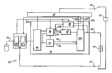
In FIG. 1, a first embodiment of three wire transmitter
50 includes sensing circuit 52 which senses process variable
54, such as pressure, temperature, level, flow, pH or the
like. Three wire transmitter 50 operates in a process control
application in the fie:Ld. Power is supplied to it from an
external energization source 56, which is typically a 6V or
12V solar battery having a limited current sourcing ability.
Consequently, transmitter 50 preferably consumes a small
amount of power. Furthermore, in many applications several
transmitters 50 are powered by the same supply, making power
consumption even more critical. In the preferred embodiment,
power drawn from the energization source 56 does not exceed
0.04 watts.
In operation of transmitter 50, an external device 59
is connected to transmitter signal output 68. A first type of
external device is a hand held communicator which sends AC
signals to transmitter 50 which select transmitter status,
performance data and PV value stored in microcomputer 64. In
response, transmitter 50 sends an AC signal representative of
the data selected by the hand held communicator. The AC
signals are communicated in the HART~ protocol, defined in
Rosemount Inc. HART~ Smart Communications Protocol Data Link
Layer Specification, but alternate embodiments of transmitter
50 communicate by other protocols.
A second type of external device 59 couplable to signal
output 68 is a controller. In one such application,
transmitter 50 provides a DC signal representative of the
sensed process variable 54 to signal output 68. The DC signal
is typically transmitted in a 1-5V protocol wherein the output
potential is representative of process variable 54, but
alternate current or voltage signalling standards can be
WO 93/06576 ~ .~. ~. e, ~~ ~) ~ ('Cf/I~592/0703~i
-4-
employed, such as .8-3.2V. This type of external device
has a characteristic input impedance typically greater
than 100Kt1 over a DC range of frequencies including DC
and extending to 20Hz. Tn another controller
application, transmitter 50 sends an AC signal
representative of the sensed process variable to signal
output 68. The AC signal is typically transmitted
according to the HART~ protocol, but other alternate AC
protocols are available.
Functions of the hand-held communicator and
the controller may be combined into a single external
device, because signal terminal 68 couples to both
devices. Alternatively, the hand-held communicator
external device or the controller external device may be
connected to signal terminal 68.
Sensing circuit 52 preferably includes a
sensor 60 for detection of process variable 54 , which in
this application is level. Typically, output of sensor
60 is an analog signal which is digitized by analog-to-
digital (A/D) converter circuit 62. Preferred low
power A/D circuits for process control applications are
disclosed in tJ.S. Patent No. 4,791,352, titled
"Transmitter with Vernier Measurement~, owned by the
same assignee as the instant application. Process
control applications typically require that the A/D
converter consume a small amount of power, have
relatively high resolution, fast update rates and employ
a minimum number of signal lines to communicate the
digitized result.
Sensing circuit 52 is powered by power
distribution circuit 63, which includes filtered 5V
supply 63a for general distribution to other circuits in
transmitter 50, 1.235V supply reference 63b, DC-DC
SUBSTITUTE SHEET
,.-.
VVO 93/06576 1 ftT/1)S92/07038
-5-
converter supply 63c for analog circuitry and 2.5V
, reference supply 63d. Distribution circuit 63 receives
power from power terminal 66, which is couplabl~
to the
corresponding power terminal of external power
supply
56. Common terminal 69 is couplable to the common
terminal of power supply 56. External device 59
need not
share power supply 56 with transmitter 50, but
must
share common terminal 69.
Communications circuit 70 includes
microcomputer 64 which receives and stores the
digitized
output of A/D circuit 62. Preferably, microcomputer
64
includes storage capability for storing constants
relating to status and performance of transmitter
50.
Alternatively, the constants are stored in an external
EEPROM and communicated to microcomputer 64.
Performance related constants relate known errors
in
sensor 60 performance as a function of the desired
process variable so that microcomputer 64 provides
a 14
bit wide digital output compensated for such errors
which is representative of process variable 54.
Compensation methods for transmitters are well
known and
documented in U.S. patent 4,598,381 to Cucci, owned
by
the same assignee as the instant application. Status
information about transmitter 50 includes the
manufacturing location, date of manufacturing and
other
pertinent information.
Pulse width modulation (PWM) circuit 72
receives the 14 bit wide digitally compensated
microcomputer output and stores seven upper bits
and
seven lower bits in '-separate registers therein.
Combinational logic in circuit 72 converts contents
of
each of the registers into two pulse width encoded
outputs, called OMSB and OLSB and shown at 74,76,
S11RSTITUTE SHEET
~' I 1. :) ~ :~ '~ ,~c-rius9zio7a3a
WO 93/06576
-6-
respectively. The magnitude of the register contents is
proportional to the width of the pulse. The magnitude
of the pulse width encoded word can be a maximum of 2',
or equivalently, 128 clock pulses long. For example, if
the magnitude of the compensated sensor output is 583,
or equivalently 10010001112, circuit 72 splits such
. output into an upper word of 1002 and a lower word of
1000111?. Circuit 72 output for the upper word, OMSB,
is a pulse of four clock cycles duration, transmitted
to within a fixed time of 128 clock cycles. In likewise
fashion, circuit 72 output for the lower word, OLSB, is
a pulse of width 71 clock cycles out of 128 cycles.
Circuit 72 is preferably designed of CMOS logic and is
an Application Specific Integrated Circuit (ASIC) in
order to reduce current consumption.
The digitally compensated microcomputer output
representative of the sensed process variable is also
coupled to modem 78 which encodes the sensor output
according to Bell 202 standard, published by AT&T in
Bell System Data Communications Technical Reference,
Data Sets 202S and 202T Interface Specification, July
1976. Modem 78 provides phase continuous modulation
according to the specification and is available from NCR
Microelectronics Division in Fort Collies, Colorado as
Bell 202 Modem ASIC, Part Number 609-0380923. The
modulated output of modem 78, signal 210, is sent to
wave shaping circuit 82 for shaping to conform to the
Rosemount Inc. HART~ Smart Communications Protocol
Voltage Mode Physical Layer Specification, Rev. 1.0-
Final, Section 7.1.2. Transmitted Waveform. Three wire
transmitter 50 may employ other communications standards
appropriate for the process control industry, such as
SUBSTITUTE SHEET
' WO 93/06576 ~ .) _~ ~~ !~ J ) PC1'/US92/07038
_7_
MOD8US~ or DE protocols. MODBUS~ is a registered
, trademark of Gould Technology, Inc. and DE is a process
industry protocol developed by Honeywell, Inc. In such
embodiments, wave shaping circuit 82 is designed to mast
,.
the signal shape requirements defined in those
respective standards.
Receive filter 84 receives requests for
performance and status data stored in microcomputer 64
from external device 59. The rec,~uest is typically FSK
.
encoded and is decoded by modem 78 before being sent to
microcomputer 64.
Digital and analog output circuit loo receives
the DC pulse width modulated signals representative of
process variable 54 and wave shaped AC signals. Circuit
100 effectively superimposes the output of wave shape
circuit 82 onto the sum of outputs 74,76 and couples the
resulting simultaneous analog and digital signals to
transmitter signal output'68. If transmitter 50 is not
responding to a request fos information from external
device 59,, and so will not transmit an AC signal
representative of the response of such request, then
transmitter 50 transmits the DC signal representative
of
the sensed process variable alone.
In FIG. 2, wave shaping circuit 82 is
detailed. An upper current mirror is formed by PNP
transistors 202, 204 and a lower current mirror is formed
by NPN transistors 206,208. Minors such as these axe
conveniently available in many bipolar integrated
circuit arrays and generally available in off-the-shelf
transistor arrays. Signal 210, the modulated output
' from modem 78, couples to wave-shaping circuit 82 and
is
a square wave having an amplitude between the potential
at common terminal 69 and substantially the same
SUBSTITUTE SHEET
wo ~3~o6s~6 ~crius~2io~o3~
w .1 .k. ~1 '~ ~! ~)
-8-
potential as at the filtered 5V supply, 63a. Signal 210
has extremely short rise and fall times, characteristic
of most CMOS devices. When the potential of input
signal 210 is at a maximum, transistors 206,x08 of the
lower current mirror are conducting and transistors
202,204 of the upper current mirror are turned off.
Similarly, when the potential of input signal 21o is at
a minimum, transistors 206,208 of the lower current
mirror are turned off and transistors 202,204 of the
upper current mirror are conducting.
When transistors in the upper mirror are
condueting,,capacitor 216 is charged. When transistors
in the lower mirror are conducting, a discharge current
flows from capacitor 216 to common terminal 69. Diodes
218,220 clamp the potential of capacitor 216. If the
potential at capacitor 216 increases toward the
potential at supply 63x, diode 218 will eventually turn
on and conduct the upper mirror current that would
otherwise have gone into capacitor 216, thus flattening
the top portion of the potential across capacitor 216.
Similarly, if the potential at capacitor 216 is
decreasing toward the potential at common terminal 69,
diode 220 will eventually turn on and conduct the lower
mirror current, thus flattening the bottom of the
potential waveform. This results in a trapezoidal
voltage waveform at the wave-shape circuit output, as
shown at 306 in FIG. 3.
The potential at which diode 218 starts
conducting is determined by the relative values of
resistors 222,224 and by the base-emitter drop of
transistors 202,204. The same two resistors and the
base-emitter drop also set the upper mirror current.
Likewise, the potential at which diode 220 starts
SUBSTITUTE SHEET
' ,,1,0 93/06576 v ~. ~. : ~ ~ ~ ) 1
I (:'t'/tJ592/07038
_g_
conducting is determined by the relative values
of
resistors 226,228, and the base-emitter voltage
drop of
transistors 206,208. The value of resistors 226,228
and
the base-emitter drop similarly determine the
lower
r
current mirror current. In the absence of diodes
218, 220, capacitor 216 would integrate these
currents to
produce a triangular-shaped voltage waveform at
the
wave-shaping circuit output. The rate of rise
of the
output of circuit 82 is determined by the mirror
current
and value of capacitor 216. The mirror current
through
each side of the current mirror is approximately
20uS
when transmitter 50 transmits AC signals and 10~S
when
not transmitting AC signals. The value of capacitor
216
is chosen to be approximately 1000 pF, so that
the
effective RC time constant of circuit 82 meets
HART
waveform requirements.
Resistors 232,234 form a resistive divider to
reduce the absolute magnitude of the potential
across
capacitor 216. The value of resistors 232,234
are
selected so as to meet the waveform specification
defined in HART~ Smart Communications Protocol
Physical
Layer Specification and are of significant resistance
to
minimize the RC time constant of the output waveform
of
circuit 82. When transmitter 50 sends AC
communications, control signal 238 from modem
78 turns
off transistor 236. Control signal 238 is preferable
because when modem 78 is idle, modem output 210
has a
high impedance which would allow the potential
at
capacitor 216 to decrease to the potential of
the
collector-emitter junction of transistor 208,
thereby
-' cresting a short glitch on output 68 when the
next
sequence of AC communications was initiated.
SUBSTITUTE SHEET
' y1 n '; ..!
W093/06576 ,~, ~ _~, r) :~ ,~ ,; PCT/US92/0703ti
-10-
The arrangement of the diode 218,220 and the
mirrors provide a sharp transition between the tamping
and the flattened part of the output waveform, shown
respectively at 302,304 in FIG. 3. As currant !low
through a diode begins, the corresponding mirror set
current is reduced by the same amount. The current that
would otherwise flow into capacitor 216 is not only
being diverted, but is simultaneously reduced. In most
circuits which utilize diode clamps, the clamp voltage
l0 has a strong dependence on temperature because of the
temperature' dependence of the potential difference
across the diode. The circuit in wave-shaping circuit
82 provides some cancellation of the diode voltage drop
variation, thus making peak-to-peak capacitor potential
216 sribstantially stable with temperature. For example,
suppose that the base-emitter potential drop of
transistors 202,204 decreases due to an increased
temperature, as would the potential difference across
diode 218. However, the voltage at the junction of
diode 218 and,resistors 222,224 would decrease. The
variation in capacitor potential 216 when diode 218 is
conducting is approximately the sum of these two
opposing variations, and is therefore substantially
constant.
The current consumption of wave shaping
circuit 82 is determined entirely by the set current and
can be made arbitrarily small, depending upon the
loading of capacitor 216. Heavier loads will draw more
current away from integrating capacitor 216,
necessitating larger mirror set currents to maintain an
acceptable waveshape. High-impedance buffer 230
provides a low impedance signal to circuit 100, reducing
current consumption of wave shaping circuit 82. Circuit
SUBSTITUTE SHEET
' WO X3/06576 i:~~ ~. ~. ~~ ~~ ~.:i ~> pC'('/11592/O~OaB
-11-
82 minimizes the high frequency energy content of the
waveform by ensuring that no sharp signal transitions
occur. This is preferable because the high frequency
energy content of the waveform contributes to AC
signalling cross-talk between multiple transmitters
having adjacent power and communication lines.
The specification for wave shaped output of
circuit 82 is given in the above referenced NART~ Smart
communications Protocol Physical Layer Specification.
The amplitude of the wave shaped signal must be between
400 mV and 600 mV peak-to-peak as measured across a HART
defined test load of 50011 in series With a 10~F
capacitor, the rise time must be between 75 uS and 100
~S when transmitting 2200Hz and less than 200 uS when
transmitting 1200Hz. The amplitude and rise time
specifications limit crosstalk, which is particularly
critical when the power connections of multiple
transmitters share the same cable.
In FIG.2, receive filter 84 includes op-amp
240 and resistor 242. Resistor 242 has a large enough
impedance so that the parallel combination of resistors
242,110 appears as an effective open circuit to the rest
of the circuitry in transmitter 50. The value of
resistor 242 must be large enough so that incoming AC
signals from external device 59 are not shorted out.
Zener 127 prevents damage to transmitter 50 circuitry if
a supply were connected to terminal 68.
Output circuit 100 passes the wave shaped
signal from circuit 82 through a band pass filter,
comprising capacitor 102, resistor 104, capacitor 106
and resistor 108, designed to pass substantially those
frequencies between the FSK frequencies 1200 and 2200 Hz
as required in the Bell 202 standard. The band pass
CI IiiCTITI1T~ CI-IFFT
WO 93/06576 ~W ~ ~.. a.~ -~ ~~ a f~T/~1592/07038
1 ~. )
-12-
filtered signal is connected to signal output 68 through
resistor 11o. ,
Circuit 100 must perform desired transmitter
functions as well as meet HART physical layer standards.
.5 The first requirement is that circuit 10o present an
output impedance between 1000 and 2000 ohms as seen
between terminal 68,69 over the HART defined Extended
Frequency Band of 500Hz to lOkHz. Secondly, it must
also present an impedance of substantially zero ohms at
terminal 68 at frequencies of 20Hz or less. Thirdly, it
must filter.signals 74,76 and provide a substantially DC
output. Fourthly, circuit 100 must provide such
filtered signals to terminal 68 at a prescribed level of
gain. Lastly, the AC signal must be superimposed on top
of the substantially DC signal and the AC signal must
have a prescribed gain.
In FIG. 4, an equivalent circuit 100 is shown
for low frequencies and DC. The resulting output
impedance at terminal 68 with respect to terminal 69 is
nearly zero, as required for transmitting the DC signal.
Resistor values 112,118,120,126 and 116 are selected so
that when OLSB and OMSB (signal 76,74, respectively) are
all zeros, the sum of the current flowing through
resistors 112,116,118 to circuit 72 and through resistor
126 towards common terminal 69 equals the current
through resistor 120, so that the potential at signal
output 68 is approximately 6.0V. Similarly, when OLSB
and OMSB are all ones, the difference between the
current flowing into the summing junction through
resistors 112,116,118 and the current through resistor
126 is substantially equal to the current through
resistor 120 so that the DC output at signal terminal 68
is approximately 0.5V. Capacitors 123,124, shown in
SUBSTITIJTE SHEET
WO 93/06576 a ~~ '' E~crnc~sn2imo:~ss
.., a. .~. .~ ~ ,a i
-13-
FIG. 2, provide low pass filtering of the inherently
noisy OLSB and OMSB signals so that the pulse width
modulation is removed and only a DC current flows into
the summing junction where resistors 118,126,112,128,120
join.
In FIG. 5, equivalent circuit 100 for higher
frequencies is shown. Several components shown in FIG.
2 axe absent from this model. For example, capacitor
124 is substantially a short circuit and effectively
removes the feedback path through resistor 12o and
isolates resistor 110 from feedback. Resistor 110
appears in series with opamp 114 output. By choosing
resistor 110 to be in the range between 1000 to 2000
ohms, the first requirement is satisfied. Capacitor
102,106 of circuit 100 become effective short circuits
so that with proper selection of resistors 104,108, a
specified gain can be achieved for the transmitted AC
signal.
FIG. 6 shows the output impedance of
transmitter 50, as a function of frequency in Hz, seen
by external device 59 between output terminal 68 and
common terminal 69. For frequencies less than fD~, the
output impedance must be substantially less than the
input impedance of DC receiving external device 59, in
order to transmit the effectively DC signal into a
minimum of 100Kf1. In general, the output impedance of
transmitter 50 is significantly lower than the DC input
impedance of external device 59 so that accuracy of the
transmitted DC signal is not compromised. For the HART
protocol, fDC is 20Hz and ZDC is substantially zero
ohms. The 100Kt1 is specified in the above referenced
HART~ Smart Communications Protocol Voltage Mode
Physical Layer Specification, Section 7.3. For example,
SUBSTITUTE SHEEI'
WO 93/Oti576 ,w (. ~. :.~ '~ ~) ~,) fCI'/tJfi92/07038
-14-
if the input impedance of DC receiving external device
59 is l0oktl and the required DC accuracy is 0.1% of the
output span of transmitter 50, then the output impedance
must be less than 100kt1 multiplied by 0.001, or 100t1 for
frequencies between 0 and 2oHz.
In FIG 7, the output impedance of transmitter
50 is shown as resistor Rout and voltage potential Vo
is the desired effectively DC output potential of
transmitter 50. Resistor Rin represents the input
impedance of DC receiving external device 59, and the
measured potential across Rin is defined as Vfn. In
order for transmitter 50 to maintain 0.1% accuracy over
the full range of possible effectively DC output
signals,
RE
YE' Voutx
Rout+RE
This is approximately equivalent to the following
equation for Rp~t much less than Rin:
1- RR°°t >0.999
E
Or, R~t~p , OO1RF
in order for transmitter 50 to transmit with 0.1%
accuracy.
For transmitted and received frequencies
~~ithin the HART defined extended frequency band (500 -
lOkIiz ) , shown at f~cl and f~c2 on FIG . 6 , output
impedance is between 100011 to 200011, so that signals
transmitted from external device 59 are not shorted out
and so signals transmitted from transmitter 50 can be
SUBSTITUTE SHEET
Hi0 93/06576 ~ ~. .) ~ ~ '~ ~~ 'J p~ ['/US92/0703f1
-15-
received at device 59. HART~ Smart .Communications
Protocol Voltage Mode Physical Layer Specification
referenced above defines the preferred output impedance
range for the extended frequency band. Alternative
communications standards dictate other impedance levels.
In FIG. 2, signal 76 is coupled to circuit 100
at resistor 112 and is connected to a current summing
junction which is controlled to supply 63b due to action
of opamg 114. Similarly, signal 74 is coupled to
circuit 100 at resistors 116,118 and is connected to the
same current summing junction. Resistor values
112,116,118 are selected so that the value of resistor
112 is approximately 128 times larger than the value of
the combination of resistors 116,118. The ratio of 128
is selected to correspond with the selection of 7 bits
(or equivalently, 128) in the lower word, represented
serially on signal 76. Accordingly, resistor 112 has
value of 8.25 Mtl and the summation of the values of
resistors 116,118 is approximately 64 kfl, although other
appropriate values can be calculated.
Because the potential at signal terminal 68 is
typically 1-5V, the 400mV - 600mV peak-to-peak AC signal
as measured across the HART defined test load of 500 t1
in series with 10 ~CF, may be superimposed on the
substantially DC potential at terminal 68 to provide
simultaneous AC communications on the effective DC
signal. The maximum peak of the simultaneous AC and DC
signal remains less than substantially the potential at
supply terminal 66 and the minimum peak remains greater
than substantially the potential at common terminal 69,
so the simultaneous signal does not saturate at maximum
and minimum potential values. Transmitter 50 outputs an
effective DC signal exceeding 5V when an error condition
ttIRSTiTIITF SHFFT
- - WO 93/06576 PCT/US92/07038
-16-
occurs and during such time, simultaneously transmitted
AC signals will create a transmitter output potential
which is flattened at the maximums and minimums of such
signal.
Although the present invention has been
described with reference to preferred embodiments,
workers skilled in the art will recognize that changes
may be made in form and detail without departing from
the spirit and scope of the invention.
SUBSTITUTE SHEET