Note: Descriptions are shown in the official language in which they were submitted.
WO 93/07664 PCT/GB92/01808
AN OP't'T GAL AMPLI FI ER
This invention relates to an optical amplifier, and in
particular to an optical amplifier which includes a doped
optical waveguide for providing gain to ogtical signals
propagating along the waveguide within an operating band of
wavelengths.
Optical amplifiers of this type are well known, and
are very attractive devices for optical communications
networks, particularly when based on optical fibre
waveguides as they are readily spliced to fibres used for
optical transmission. It 'appears likely that they will
become widely used in place of opto-electronic repeaters in
long distance optical fibre lengths, fox example. Some
such optical amplifiers have a gain peak within the gain
spectrum. For wavelength division multiplexing, a gain
spectrum which has a gain peak is not ideal where cascades
of amplifiers are to be used as this may result in large
differences in gain across the wavelength band. If such
large differences are to be avoided, it is necessary to
operate in a band of wavelengths which does not include a
gain peak. This reduces the useful gain band of an optical
amplifier.
An object of the present inventian is to provide an
optical amplifier with a flatter gain spectrum.
The present invention provides an optical amplifier
including a first, doped optical waveguide for providing
gain to optical signals propagating along the waveguide
withi n an operating band of wavelengths, the waveguide
having a gain peak within the operating band, characterised
in that the first optical waveguide is optically coupled to
a waveguide filter which comprises a second optical
waveguide having an overlaid grating constructed and
configured so that the waveguide filter provides loss in
transmission substantially at the wavelength of the gain
3 5 peak.
_____~.-._W~~...........,~.~..-~..-.-.~.,-
.r.".t..v..,s.ro.awssav~.r...a,...rr~R...-rmc._.....,
l...n.....S~St.Yttt:LS.....l.srF..F .fr .l..y'~".~..,., .. .siev.a....u~ts
t".....w .. .a... ...
WO 93/07664PCT/GB92/01808
_ 2
The waveguide filter can provide flattening of the
gain spectrum because the transmission profile of such a '''
grating, overlaid on a waveguide, exhibits attenuation of '
optical signals to wavelengths shorter than the resonant
reflection wavelength of the grating.
Preferably the grating is configured to have a
resonant reflection wavelength substantially equal to, or
greater than, the wavelength of the gain peak, so that the
short wavelength attenuation associated with the filter
will provide attenuation to the gai n peak, thereby
producing a flatter gain spectrum. Hence it is possible to
use a grating, which when used as a narrow-band reflection
filter has a reflection bandwidth of say 1. 28 Angstroms, to
obtain satisfactory flattening over a relatively 'broad
spectrum gain peak of 20nm for example.
Advantageously the grating is angled relative to the
second waveguide so as to substantially suppress counter-
propagating radiation at the resonant reflection wavelength
of the grating. The operation of the amplifier is thus not
disturbed by optical signals at the resonant reflection
wavelength being reflected back into the first doped
waveguide. Counter-propagating radiation is, in general,
undesirable in an optical communications system since it
requires optical sources in the system to be optically
isolated, and may contribute to crosstalk in duplex
systems.
As the grating is rotated away from a position where
the grating lines are perpendicular to the waveguide, the
effective pitch of the grating experienced by optical .
signals travelling in the waveguide will increase. This
will cause the resonant reflection wavelength of the
grating, that is the wavelength at which the Bragg
condition is met, to increase, and the wavelength range at
which optical radiation is coupled out of the second
waveguide to decrease. Hence the transmission loss of the
WO 93/07664 PCT/GB92/01808
- 3 -2119746
waveguide filter can be chosen so as to optimize the gain
spectrum of the amplifier.
The optical amplifier may be made from a doped optical
fibre but may be any other type of optical waveguide, for
example a planar waveguide.
A particularly convenient form of optical waveguide
for the waveguide filter is an optical fibre having a
substantially D-shaped cross-section (commonly and
hereafter referred to as a "D-fibre"). Such a fibre has a
planar surface close to the waveguiding core of the optical
fibre so that an optical grating formed on this pl--anar
surface or pressed against the surface will interact with
an optical field propagating through the fibre to provide
the required diffraction. Conveniently the D-fibre may be
1~ mounted in a thermoplastic substrate. A method of so
mounting a D-fibre is described in the applicant' s
published patent application WO 89/11969 published 14th
December 1989.
The grating maybe formed by etching the grating into
a silica wafer using known electron beam lithography
techniques, and the waveguide filter may then be formed by
pressing the silica wafer against th~ waveguide.
A specific embodiment of the present invention will
now be described, by way of example, With reference to the
accompanying drawings, in which:
Figure 1 a graph of the spontaneous emission
measurements on an erbium-doped fibre amplifier which forms
part of the embodiment of Figure 2;
Figure 2 is a schematic diagram of an optical
amplifier according to the present invention;
Figure 3 is a graph showing the transmission
characteristics of the grating filter of the embodiment of
Figure 2; and
Figure 4 is a graph showing the gain spectrum of the
optical amplifier of Figure 2.
WO 93!07664 PCT/GB92/01808
4
Referring to the drawings, Figure 1 shows the gain
spectrum of an erbium-doped optical fibre amplifier. This ;
shows a gain peak centred at about 1. 54~m, the gain peak
reducing the usable part of the gain spectrum to
wavelengths longer than the long wavelength side of this
gain peak, that is to about 20nm.
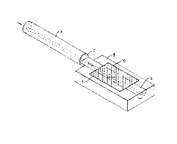
Figure 2 shows a D-fibre 4, which may be made by
removing a section of cladding from an optical fibre
preform to leave a flat surface close to the core. This
preform is then drawn to give a long length of single-mode
fibre with a D-shaped cross-section. A short length (of
the order of 20mm) of this D-fibre is then fusion spliced
to a standard single-mode fibre 6, at a splice 7, and then .
press moulded, against a heated optical flat 4not shown),
into a polymer thermoplastic substrate 8, as described in
the above-referenced patent application.
A grating 10 (see Figure 2) is then defined using .
electron beam lithography on a silica wafer 9 coated in
photoresist. The grating 10 is subsequently etched into
the silica itself to give a surface relief structure with ,
a depth of about 0. 25~am and a pitch of about 0. 532 Vim.
To construct the filter, the D-fibre substrate 8 is
mounted in a brass package (not shown), and the grating is
placed in contact with the flat surface of the fibre 4 at
an angle of about 3°. A layer of silicone rubber is used
between the grating 10 and the lid of the package so that
the grating is pressed into contact with the fibre 4 when
the lid is screwed down.
Fibre grating devices such as couplers and reflection
filters have been reported previously (see for example
Yennadhiou, P and Cassidy, S A: " D-Fibre Grating Reflection
Filters" OFC 1990). For such a reflection filter, the
grating lines are perpendicular to the fibre, and give a
Bragg reflection which is coupled into the counter
propagating fibre mode. The grating of the present
invention is used in transmission mode, and is configured
..,,
:.,: ...,
.i ::
~,::5 '
\ . L.
.~..
~.'s
... -,,' 1~'.' ~.
;:-~. ., ':..'~....,.... .. , ,::., ... : ::.......; : . .-~.,:~.~~ ,
.'.'~..... .~,~ ... ... ~: .. .. .-.:....t.k......... .
WO 93/07664 PGT/GB92/01808
_ 5 _
2~1~~'~40 .
to suppress the resonant reflection wavelength of the
grating. Light at wavelengths shorter than the resonant
reflection wavelength is coupled out of the fibre, either
up through the ~ grati ng its el f i nto radi ati on modes , or down
into cladding modes. This results in a transmission filter
with loss at he wavelengths which are coupled into
radiation or cladding modes, and hence which provides loss
at shorter wavelengths than the resonant reflection
wavelength. The wavelength at which this loss occurs is
dependent on the grating pitch and on the angle of the
fibre 4 to the grating 10, and can thus be chosen to
;.,
coincide with the gain peak 2 of the amplifier.
In this embodiment the~pitch of the grating is chosen
to be about 0.532 ~m to give a resonant reflection
wavelength of about I.54 ~m when the grating lanes are
perpendicular to the waveguide. The resonant reflection
wavelength is increased by about 2nm by rotating the
grating by about 3° relative to the waveguide. At an angle
of about 3° the counter-propagating radiation at the
resonant reflection wavelength was found to be
substantially supressed.
Figure 3 shows the transmission characteristics of the
waveguide filter of Figure 2, these characteristics being
determined by monitoring the transmission of the filter
using an FLED and optical spectrum analyser. Tuning of the
resonant reflection wavelength. results in a slight
reduction of filter depth, because the interaction length
of the grating (that is ,to say the length of the fibre in
contact with the grating) is limited by its width, which in
this case is approximately imm.
Once a suitable filter transmission characteristic is
obtained; it can be tested by measuring the spontaneous
emission from a short length of the optical amplifier, in
this case an erbium-doped silica fibre, pumped with a 980nm
3S diode laser (not shown).
WO 93/07664 PGT/G1392/01808
-s-
2119rr46
Figure 4 shows the spectrum after the filter is
spliced onto the end of the doped fibre. Clearly, the
filter has improved the flatness to within about 0.5 d8
over a 30nm span. The excess loss of 4 to 6 d8 is mostly
due to D-fibre to circular fibre splice losses. This could
be reduced, as a more typical loss for a D-fibre substrate
i s 2 d8.
It will be apparent that modifications to the specific
embodiment can be made. In particular the preferred angle,
of 3°, of the grating to the second waveguide, although
theoretically predictable, is ultimately chosen for a
particular type of amplifier and system by trial arid error.
As will be evident to the skilled person in this field the
choice will depend, among other criteria, on the refractive
index profile of the D-fibre, the structure of the grating,
the distance of the core of the D-fibre from its planar
surface, the type of doped waveguide, the wavelength of
operation of the system, and the susceptibility of the
system to counter-propagating radiat~,on. It is estimated
that the useful range of angles is from 1° to 10°.
!
,"
~r.rr,z ~,-r~ t ?f~-..~ .:.:e...
->: a r. '-, r: r~ , ~~ ..°
r.r-. .. .'rte . "Vr, .L
.. r . .. .. ..., r.:,:ar . . r .~.r . . . .v . ..
es~s.,._ ..... . . _..:.n...._......s. 6 ..'.':. n.s. ....;~u_......J~'hlG,
aC...... _.,._F..u...a.,y'~dr~yrr:.:... ,...... .4~SR,....'n..e.'~v...
r.n..9:.............,d..: <.,..:..r... ... .,...~ ........ ,t.. ."... , . ,