Note: Descriptions are shown in the official language in which they were submitted.
LD I 0S24
2~1~8~3
FIELD (:)F rl
The present invention relatles to a power supply circuit for a gas
discharge lamp, which is contained with~n a resonant load circuit supplied with
- 5 bidirectional current through th operation of a pair of switches. More
par~icularly, the invention relales to such a power supply circuit whereill control
sigrlals for the mentioned pair of switches are produced by fe~baek circui~y
that is responsive to a feedback signal represent~ng a current ~n the resoDa~t
load Cil~Uit.
BACKGROUND OF l~IE INVlENTION
A gas discharge larnp, such as a fluorescent lamp, typically utiliæs a
power supply circuit to convert an a.c. Iine voltage to a high frequency
bidirectional voltage which is ~mpressed across a resonant load circ~it
conta~ning the gas dischar~e lamp. T~e resonant load circuil includes a
resonam inductor and a resonant capacitor ~or determining the freque~y of
resonance of current in the resonant load circuit. l`he power supply circuit
includes a series half-bridge converter having a pair of switches that alterDa~gly
COMect one end of ~he resonant load circuit to a d.c. bus voltage and then to
a ground, thereby impressing ~he mentioned bidirectior~l voltage across the
resonant load circuit.
A prior arl power supply circuit of the foregoing type is disclosed in co-
pending U.S. palent application Serial No. 08/020,275 ateorney docket number
LD 10,5~3), filed February I$, 1993, enti~led "Elec~ronis Ballast Arrangemen~
For A Compact Fluorescen~ Lamp," by Louis R. Nerone, the presgllt inventor,
and assigned tO the present assignee and which is herein incorporated by
reference. The disclosed power supply circuit utilizes feedbaclc circuitry ~or
comrolling the mentioned pair of swi~ches of the series half-bridge converter.
The feedback circuitry operates in respo~ie go a ~edback signal represe~ing
a currem in the resonant load circuit.
. . . . .
LD I 0524
21~9~o3
~ 3y relying on feedback circuitry to control the switches, the power
supply c~rcuit of the foregoing pateDt application avoids the expense and bulk
of extra circuitry for switch control. However, it would be desirable to reduce
the level of variations in launp power and lamp cwrent that occur due to
variations, for instance, in the line vol~age.
A gas discharge l~np such as a low pressure fluorescent lamp, and the
power supply or ballast circui~ uranlJement as it is more commonly known, are
presently being offered on a wide scale comme~ial basis in a co~lguration that
lends itself to being a viable energy efficient lorlg life ~eplacemellt for a
10 conventional incarldescent lamp. Compac~ fluorescerlt lamps as ~ey are
comunollly known utilize a compact, typiçally multiple axis discharge vessel
containing a gas ~111 which includes a mLl~ture of mercury and a rare gas such
as krypton or argon. The ballast circuit is conta~ned in a housing base having
an Edison Type screw base which can be installed in a conventio~l lamp
15 s~cket. Because of the desirability of utili~iQg such compact fluoresce~ lamps
as replacements for convention~l incalldescent lamps, it is necessary that ~he
ballast circuit and the housing base occupy such a small space as would allow
insertion irl most light fixtures. To achieve this it is impo~ant that the siæ alld
quantities of the cornponents tha~ comprise the ballast circuit are kept to a
20 miI~imum. For a discussion of the physical characteristics associated with
disposing the ballast eircuit within the housing base, reference is made to
commonly assigned U.S. Patent Application Serial No. 07/766,608 ~lled on
February 26, 1991 bY MjnarGZYk et ah which is herein incorpora~ed by
re~erence.
In addition tO the desirability of utilizing this improved power supply
circuit for the popular compact fluorescent lamps which have an electroded
arrangement ~or exciting the discharge, it would be advantageous if this circuitarrangement could be utilized on an elec~rodeless fluorescent lamp where the
discharge is excited by introduction of an RF signal which is coupled to the
30 medium through an excitation coil disposed in close proximi~y to the medium.
: - - ., - . ~
LD I OS24
~g~03
Accordingly, it is an objec/ of the present inven~ion to provide a power
supply circuit ~or a gas discharge lamp which is contaiDed within a resonant
load circuit, wherein the power supply circuit utilizes ~eedback circuifry for
5 controlling switches of a series hal~-bridge converter and wherein lamp power
and Jamp curren~ are less subject to change ~n response t~ a variation in, e.g.,line voltage, than is ~he case for the pnor art circuit mentioned above.
A furlher object of the invention is to achieve ~e mentioned reduction
of change in lamp power and larnp current due to var~a~ions ~n, e.g., line
10 voltage, without adding component~y to the power supply c~rcuit thereby
avoiding increased cost and siæ variables.
The foregoing objects are realized by a power supply circuit for a gas
discharge lamp, which includes means for providing a d.c. bus voltage on a bus
conductor, and a resonant lamp ci~uit. rne reso~t lamp circuit Lncludes a
15 gas discharge lamp, a first resonant impedance in senes wi~ the gas dischargelamp, ~d a second resorlant impedance substanaially ~n parallel wi~h the gas
discharge l~np. The resonant load eircuit operatgs at a resonaJIt frequen~y
determined by the values of the first and second resollant impeda~ces. Fur~her
included is a series half-bridge conve~er for impressing across the resonant
20 load circuit a bidirectional voltage, and the~eby inducillg a bidirectiorJal cu~Tent
in the resonant load circuit. The converter comprises first and second switches
that are serially connected between the bus conductor and a ground conductor,
that have a cornmon node coupled to a fîrst end of fhe resonant load circui~ andthrough which the bidirectional load current flows, and that have respective
25 control tenninals for controlling the conduction states of the switches. Means
are provided for generating a feedback signal representing current in the secondresonaM impedance. A feedback means, responsive to ~e ~eedback sign.al,
provides respective control signals on the control lenninals of the first and
second switches. The feedback means con~rols the switching of the swi~ches
30 in such maculer as to reduce a phase angle between fhe bidirectional voltage and
- ,.
LD 10524
2~19803
the bidirectional current when the feedbaclc sigrlal ~ncreases, and vice-versa.
In the foregoing power supply circuit, lamp power and lamp currenl are
less subject t9 variation as line voltage varies. The ci~uit, moreover, can be
cons~ucted without additional componentry beyond thal contained in the pl~or
5 ~ circuit described above.
BR~EF DESCRIPTION O:F THE DE~AWING F.IG~ES
The foregoing, and further, objects and advantages of the ~ventio~ will
become apparent from the following description taken in conjunction with the
drawillg, ~n which:
Fig. 1 is a schematic diagram, partially in block ~orm, of a power
supply circuit including feedback circuitry for controlling the collduction states
of a pair of switches of a half-bridge converter.
Fig. 2 is a c~rcuit diagram of a prior art resonant load circuit that can
be used in the power supply circuit of Fig. 1.
Fig. 3 is a simplified graph showing the variation in the cosine of a
phase angle between a bidireG~ional voltage across, and a biduectiorlal urrent
through, the resonant load circuit of Fig. 1 versus a feedback current used in
the power supply circuit of Fig. 1.
Fig. 4 is a circuie diagr~n of a reson~nI load circuit according tO the
invention, ~hat may be used in the power supply circui~ of Fig. 1.
Fig. 5 is a simpli~led graph showing the v~riation in lamp vol~age versus
lamp power.
Fig. 6 is a circuit diagram of a snubber & gate speed-up circuit that may
be used in the power supply circuit of Fig. 1.
Fig. 7 shows an alternative embodiment of a resonant load circuit,
according to the invention, that may be used in the power supply circuit of Fi~.1.
DETAILED DESCRIPTIC)N OF THE PREF~ERRED EMBQDIMENTS
. ~ ~ . ".. . .
. ~ , , ., ~, . ., .. . ~
LD 10524
21 ~ 9803
In the drawing figures, in which like re~erence numcrals or characters
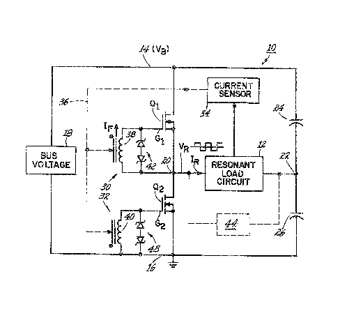
refer ~o like parts, Fig. I shows a power supply circuit 10 for a resonant lo~d
circuit 12. Resonant load circuit 12 may include a gas discharge lamp, as
~urther described below. Electncal power for resonant load circuit 12 is
5 provided by a bus voltage VB impressed between a d.c. bus conductor 14 and
a ground conductor 16. Bus voltage VB is provided by a bus voltage generator
18, typically comprising a conventional full-wave rectifier, for rectifying a.c.voltage from an a.c. source, or line, voltage (rlot shown). Bus voltage
generator 18, oplionally, may include a power factor correction circuie, as is
10 conventional.
Power supply circuit 10 impresses a bidirec~ional, resona~t load voltage
VlR across resonant load circuit 1.2, from left-shown node 20 to righl-shown
node 22. As shown in Fig. 1, resonaM load voltage VR approximates a squ~
wave. Bidirectiorlal, resonant load vol~ge VR, in ourn, induces a bidirectional
15 resonant current IR through resonant load circuit 12.
To generate resonant load voltage VR ~rom d.c. bus voltage VB on d.c.
bus 14, power supply circuit lQ includes a sencs half-br~dge converter,
including series-colmected MOSFETs (Metal-Oxide-Semiconduc~or Field-Effect
l`ransistors), or other switches, Ql and Q2 The drain of MOSFET Ql is
20 directly connected to d.c. bus 14, and its source is cormected to the drai~ of
MOSFET Q2 at node 20, which is common to switches Ql and Q2 The drain
of MOSFET Q2 is connected to gro md 16. The conduc~ion states of
MOSFETs Ql and Q2 are determined by respective control vol~ages on the
respecLive gates Gl and G2 of the MOSFETs. In brief overview, bidirectional,
resonant load voltage VR is generated by alternately connecting common node
20 to d.c. bus 14, which i5 at bus voltage VB, via MOSFET Q1~ and then to
ground 16, via MOSFET Q2 Serially connec~ed "bridge" capacitors 24 and
26, connected between d.c. bus 14 and ground 16, main~ain right-shown node
22 of resonant load circuit 12 at approximately 'h of d.c. bus voltage 'VB.
Control signals are provided on gates Gl and G2 of MOSFE'rs Ql and
, . . , .
-,
LD l 0524
21~9803
Q2 by respective feedback circuits 30 and 32. Feedback circuits 30 and 32 are
responsive to a current from pa~ of resonallt load circuit 12 that is sensed by
culrent sensor 34. CulTent sensor 34 provides feedback circuits 30 and 32 with
a feedback signal represeming the mentioned current in resonant 10ad circuit 12,S via schematically shown couplin~ 36.
Fig. 2 shows a prior art reso~nt load c~rcuit 12 that may be used in the
power supply circuit 10 oî Fig. 1. This privr art resonant load circuit is
described herein to ~acilita~e understanding of the present ~nvention.
In prior art circuit 12 (Fig. 2), a gas discharge lamp is represe~ted as
10 a lamp resistance RL The gas discharge lamp may be of the low pressure
variety (e.g. fluorescent), or of the high pressure variety (e.g. metal halide or
sodium~. In order to es~ablish a fundamen~al frequency of resonance in circuit
12, a resonant inductor LR and ~ resonant capacitor (:R are included in the
circuit. Resonant capacitor CR is shunted across lamp resistance RL~ and
15 resonant inductor LR jS serially coMected to the ~hus-paralleled lamp resistance
RL and resonant capacitor CR. A current-se~sing winding 34, in series with
resonant inductor RL, embodies current sensor 34 of ~ig. 1.
CulTent-sensing winding 34 is mutually coupled ~o inductor w~ndings 38
and 40 of Fig. 1, as indicated by coupling 36. Wind~ngs 34, 38 and 40 are
20 poled as indica~ed in the drawing by dots, or, alterDatively, may be oppositely
poled. As shown, inductor windings 38 and 40 are coupled tO each other wi~
opposing polarities. In this manner, MOSFETs Ql and Q2 are switched on
(i.e. made conductive) in an alternating manner. Thus, MOSFET Ql conducts,
and impresses d.c. bus voltage VB on node 20 while MOSFET Q2 is off; and
25 then MOSFET Q2 is switched on, to cormec~ node 22 to ground 16 while
MC)SFET Ql is of~.
Wilh inductor windings 38 and 40 coupled with opposing polarities, the
operation of feedback circni~s 30 and 32 will be understood from describing
only circuit 30, for instance. In feedback circuit 30, a feedback current IF is
30 generated by inductor wind~ng 38 in response, for example, to resonant load
- .. , .. , . . .. . ,.. ~ . ,
LD I 0524
2~9~
curren~ IR in induclor winding 34 of prior art Fig. 2. Shunted across inductor
winding 38 is a pair of back-to-back (i.e. cathode-to~athode) connec~ed ze~Pr
diode~ 42. Zener diodes 42 clamp the voltage on gate C;l (with respec~ to n~e
20) at a positive or a negative level with a timing d~term~ned by the polar~
S and amplio~de of feedback current IF. An inherent ga~e capacitance (not
shown) between gate Gl and node 20 also influences tlhe behaviGr of feed~ack
c~r~uit 30.
A snubber & gate speed-up circuit 44 may be corlnected across resonant
load circuit 12, as described below iD cormection with Fig. 6.
The power consuuned by the gas discharge lamp ~represen~d by lamp
resistance RL in Fig. 2) is dependent on the timing of when zener diodes 42
switch ~he polarity of voltage on gate Gl. Such ti3l~ng detennines a phase
angle between bidirectional, resonant load voltage VR and bidirectiorlal,
resonant load current IR. These values dete~e ~he approxima~e power
lS consumptivn of the lamp, according to the ~ollowing equation:
PL ~ V* X IR x cosine e eq. (I~
where ~ indicates propo~ionalily;
VR' is the pealc value of resonant load voltage V~, be~veen
nodes 20 and 22;
IR' is the peak value of resol~ant load eurrent IR; and
e is the angle of phase difference between ~he fundamental
frequency components of reson~nt load voltage VR and resonant
load current IR.
An increase in ~he resonant load voltage VR, due, ~or instance, to a line
voltage increase, proportiona~ely increases the max:imum value of resonant load
2~ voltage, VR'. From equation 1, above, it can be seen that lamp power PL
proportionately increases. (This proportionate increase due to increasing line
voltage also holds true for the present inv ntion, described below~)
Additionally, as bus voltage VB increases due to a line vol~age increase, for
LD 10~24
8 0 3
ins~ce, resonant load culTent IR (Fig. 2) also ~creases. IJsing the location
for sens~ng culTent in prior art resonant load circuit 12 (Fig. 2), feedback
curren~ IF in feedback circuit 30 (Fig 1), in ~ increases.
An increase in feedback cu~Tent IF~ in turn, influences the t~g of
S when zener diodes 42 cl~np gate G1 to either a positive, or a nzga~ive, voltage,
which aff~cts the angle ~3 contamed in equation 1 above. The relationship
betwee~ the cosine of angle ~ ampli~de and the amp1itude of feedback current
IF in feedback circuit 30 is depicted by a simplified curve 45 shown i~ Fig. 3.
As Fig. 3 indicates, increasing ~eedback current IF results in an increasing
10 cosine of angle ~3. In terms of equation 1 above, an ~nerease in bus voltage VB
not only propor~iona~ely increases th~ maximum resonant load voltage VR~ but
also incneases the cosine of angle ~3 when using the position~ng of current-
sensing inductor winding 34 of pri~r a~ Fig. 2.
The present invention is par~icularly dire.ted towards reducing the
1~ componerlt oî increased lamp power arising from the cosine of angle ~3 term in
equation 1 above. Fig. 4 shows one embodime~t of a resonant load circuit 12
that can be used in inventive csmbination with power supply circuit 10 of Fig.
1. Fig. 4 shows lamp resistan~e RL, r~sonaIIt capæilor CR and resonant
induetor L~ in a generally similar eir~uit alTangement as shown in Fig. 2.
20 However, in Fig. 4, currerlt-sensing winding 34 has beell reloca~ed to form aserial circuit with resonant capacitor CR, which circuit is substantially in
parallel with lamp resis~ance RL The placement of current-sensing winding 34
in Fig. 4 takes advantage of the pro~r~y of a gas discharge lamp of decreas~rlg
in voltage with increasing power consumption, over a normal operating range.
25 This relation is shown by the negative slope of a simpli~led curve 46 in Fig. 5,
plo~ting voltage across a lamp, VL, with respect to lamp power PL. Such
decreasing voltage wi~h increasing power is related to a decreasing lamp
re~sist~nce RL with increas~ng lamp power PL.
3Returning to Fig. 4, an increase in d.c. bus voltage VB (Fig. 1) due to
30 a line pernlrbation, for instance, tends to increase lamp power. However, since
: ,. , , ~ , . . :,
'~ ' ' '
,
.
LD I 0524
2~9~1~3
lamp vol~age VL decreases. as shown in Fig. 5, the current sensed in current-
sensing wind~ng 34 correspondingly decreases. With the proportiorLate feedback
curren~ IF also decreasing, the curve of Fig. 3 indicates that the cosine of angle
e also decreases. As a result, an increase ~n lamp power PL due to increasiIIg
5 line voltage is limited by a concurrent decrease in the cosine of angle e ~m
of equation 1 above.
For a fluorescçnt lamp rated at 11 watts, with a ~ l~nen output at a
nominal line voltage of 230 volts a.c., use of ~he pnor art resonant load circuit
12 of Fig. 2 resulted in a ratio of the change iD illpUt power (a measl~re of lamp
10 power) to the change in line voltage of 1.61. Thus, a ten percent increase inline vol~age results in a 16.1 percent increase in ~nput power. In contras2,
using the inven~ive arrangement of Fig. 4, the change in input power ao the
change in input voltage, for an otherwisf~ identical circuit, was 0.97, a
considerable decrease. The foregoing cha~ge~ power ~o chal~ge-in-line voltage
15 ratio expresses the sensitivity of l~np power to l~ne vol~ge.
A decrease in the ratio of the ch~ge in lamp eurrent to the change ~n
line voltage was also observed. The prior art circuit of Fig. 2 yielded such
change-in-current to change-in-voltage ratio of 2.89, whereas ~he inventi~e
cireui~ of Fi~. 4 yielded a markedly decreased, corresponding ratio of 1.25.
20 The foregoing change-in-lamp culTent to ehange-in-line vol~age ratio expresses
the sensitivity of lamp current to line voltage.
The decreased power and culTent sensitivities to changes in line voltage
assures that a gas discharge larnp will be less stressed from changes in line
voltage, as well as from ehanges in the values of the components of the power
25 supply circuit (e.g. a change in the inductance value of resonant inductor RL).
Longer lamp life results.
The above-meMioned sensitivity values were obtained from a e~cuit
using IRFR310-model MOSFETs Ql and Q2 from the International Rectifier
Corporation of Fl Segundo, California under ~heir ~rademark HEXFET. I~e
30 upper and lower diodes of the ~ener diode pair 42 (Fig. 1) were respectively
.~ .
~ -. , ~ . -
LD 10524
2 1 ~
ra~ed at 7.5 and 10 vol~s. A corresponding back-to-back æner diode pair 48
of feedback circuit 32 had the same .res~ctive values. Inductor w~nding 34 of
the prior art resonant load circuit 12 (Fig. 2) had 4 tu2ns, and the w~ding 34
of ~he inventive circuit of Fig 4 had 16 turns. The number of turns for each
of inductor windings of 38 and 40 was 40. Resonant capacitor C~ of bo~h
prior art Fig. 2 and inveMive Fig. 4 was rated at 2.2 nano~arads. ~esonant
inductor CR of both prior art Fig. 2 and Fig. 4 was rated 1.2 millihenries.
Bridge capacitors 24 and 26 were both rated at 47 narlofarads.
The above-mentioned comparison was performed with a power supply
10 circuit lû (Fig. 1) utiliziDg a snubber & gate spe~-up cir~uit 44, as show~ in
Fig. 6. The mentioned reduction ~n inpu~ power and lamp current sensitivities,
howeYer, are achieved irrespective of the presence or absence of snubber &
gate speed up circuit 44.
Snubber & gate speed-up circuit 44 is con~cted between nodes 20 and
1~ 22, and hence in parallel wi~h r~sonan~ d circuit 12. C~rcuit 44 comprases,
in serial connection, an inductor winding 50, a capacitor 52 and a resistor 54.
Wind~ng 50 is mutually coupled to cu~Tent-sensing winding 34 of ei~her of prior
art Fig. 2 or inv~ntive Fig. 4, and had 5 turns. C~pacitor 52 had a value of
470 picofarads, and resistor 54 a value of 22 ohms. Resistor ~4 serves to
20 reduce parasieic iMeraCtion between capaci~or 52 and o~her reac~anees coupled eo it.
Capacitor 52 operates, first, in a so-called snubbing mode, wherein it
stores energy ~rom resonant load circuit 12 during an in~erval in which one of
MOSFETs Ql and Q2 has turned off, but the other has no~ yet turned on. The
25 energy stored in capacitor 52 is thereby dive~ed from MO~FETs Q1 and Q2~
which, in the absence of snubbing capacitor 52, would dissipate such energy in
the form of heat while switching between conductive and non-sonductive states.
Further details of the snubbing role of capacitor 52 are described in co-pendingU . S . paterlt application Serial No. û8/0~0,275 ~atIorney docket no. LI3 10,583),
30 filed February 18, 1993, enti~led "Electronic Ballase Arrangeme~ for a
.:
.. .: . - . -
.
:.~
.
. ~ . . .
LD 10524 2119 8 0 3
Compact Fluorescent Lamp"~ by Louis R. Nerone.
Capaciltor 52, secondly. operates to increase the speed of SWitGhing of
MOSFETs Ql and Q2 In fhis role~ capacitor 52 erea~es a speed-up pulse whe~
a rising current in the capaci~or, induced ~n wind~ng 50, occurs. The nsing
5 culTent is induced in winding 50 fro]m rising current in current-sensing winding
34 of pnor art Fig. 2 or inventive Fig. 4. Further details of this gate speed-uprole of capacitor are described in the forego~ng paten~ application of Louis R.
Nerone.
Fig. 7 shows another inventive resonant load c~rcuit 12, di~fenng ~rom
10 the inventive Fig. 4 circuil in that the locations of resonan~ capacitor CR and
resonant inductor LR are interchanged. In the Fig. 7 cincuit, current through
current-sellsing winding 34 decreases, as does the current in current-sensmg
winding 34 of the Fig. 4 ci~uit, wi~h an inc~ase in line voltage. This is due
to the decreasing voltage across the laanp VL wi~ increasing lamp power, as
shown in Fig. 5. The Fig. 7 circuit, therefore, exhibits the same phenomenon
of feedback current IF in feedback cireui~ 30 (Fig 1) decreasi~g with increasi~gline voltage, to achieve a lower value of ~e cosine of angle e. As deseri~gd
in connection wi~h equation 1 above, a decrease in such cosi~e tenn reduces the
overall ~ncrease in lamp power.
While the invention has beerl descnbed with respeet to specific
embodiments by way of illustration, many modi~lcatiolls and changes will oecur
to those skilled in the art. For instance, digital circuilry could perform various
of ehe functions in the above-deseribed power supply eircuie ~hat are described
herein as performed by discrete components. It is therefore, to be understood
that the appended claisns are intended to cover all such modifications and
changes as fall within the true spirit seope and scope of the inverltion.
; . . . . .