Note: Descriptions are shown in the official language in which they were submitted.
CA 02119841 2001-09-12
The present invention generally relates to a write
once type information recording medium such as an optical
memory card. More specifically, the present invention is
directed to a method and apparatus which is capable of
formatting a write once type information recording medium
with increasing storage efficiency, and which has the
capability of correcting burst errors, to a write once
type information recording medium formatted in accordance
with the above-mentioned format, and to a method and
apparatus for writing data to or reading data from such a
write once type information recording medium.
There is a need to increase data recording
density in order to economically record
data on an information recording medium. However,
when the data recording density is increased, errors
occurring in the reproduced data can be increased because
of, for instance, defects in the recording medium.
In general, to reduce errors in the reproduced data,
an error correction code is~added to the data during a
data recording operation so as to perform the error
correction. There are typically two different types of
errors occurring in the reproduced data, namely, random
errors occurring at random, and burst errors occurring in
a continuous manner. Once a burst error occurs, it can
hardly be corrected owing to large . continuous errors
included therein.
To make error correction feasible, interleaving is
- 1 -
carried out in a conventional information recording
system. That is, a series of data is subdivided into a
large number of data segments which will then be
distributed into the recording medium. In this case, even
if positionally continuous errors occur on the recording
medium due to defects thereof, the ex:rors are not
continued on the reproduced data. As a result, these
errors can be corrected as random errors.
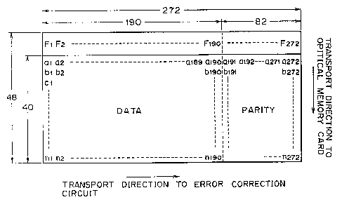
Fig. 1 schematically represents an example of the
conventional interleaving technique. In accordance with
the conventional interleaving method,, 272 "synchronization
signals for a frame and bit" (simply, referred to
"synchronization signals") are first arranged, each of
which is composed of 8 bits, for instance, and indicated
by symbol "F" as illustrated in Fig. 1. Subsequently, a
272-bit packet "a", a 272-bit packet "b", a 272-bit packet
«c~f, ---, a 272-bit packet "n" are arranged in parallel to
each other, as illustrated in Fig. 1. The first 272-bit
packet "a" contains 190-bit data consisting of al, a2,
, and a190, and an 82-bit error correction code consisting
of a191, a192, ---, and a272. Similarly, the second 272-
bit packet "b" contains 190-bit data. consisting of bl to
b190, and an 82-bit error correction code consisting of
b191 to b272, and the third 272-bit packet "c" contains
190-bit data consisting of cl to c190, and an 82-bit error
correction code consisting of c191 t:o c272. Also, the
final 272-bit packet "n" contains 190-bit data consisting
of n1 to n190, and an 82-bit error <:orrection code
- 2 -
CA 02119841 2001-09-12
consisting of n191 to n272.
. The 8-bit synchronization signals and the plurality
of packets, which have been arranged in the above-
described manner, are read in the direction indicated by an
arrow shown in Fig. 3 as follows. The reading operation
is carried out sequentially from the synchronization
signal F, the first bit a1 of the first packet "a", the
first bit bl of the second packet "b", the first bit cl of
the third packet "c", and up to the first bit n1 of the
last packet "n". Next, the reading operation is performed
sequentially from the synchronization signal F, the second
bit a2 of the first packet "a", the second bit b2 of the
second packet "b", the second bit c2 of the third packet
"c", and up to the second bit n2 of the final packet "n".
In this reading manner, the packets up to the 272-nd bit
n272 of the last packet "n" are read out, and then they
are rearranged as a bit stream as shown in Fig. 2.
Conventionally, such a rearranged bit stream is recorded
on the information recording medium.
The bit stream, beginning from the synchronization
signal "F" through al to n272, as shown in Fig. 2 is
called a "sector". In the conventional recording medium
with the above described recording format, the larger the
number of interleaving processes, (namely, the
greater the quantity of packets) , the more error
correction can be performed with respect to the burst
error. However, the increasing number of interleaving
processes requires a longer sector. Since various lengths
- 3 -
~9
of data are normally recorded in a single sector, a long
sector may include a useless storage capacity in case of
short (small) data. Consider now the case where short
data having three packets is stored .into a long (large)
sector. As shown in Fig. 3, even if (8+273)X3 bits data
from F, a1, b1, c1, F, a2, b2, c2, ---. up to F, a272,
b272 and c272 is recorded in this large sector, a
substantial sector portion will remain as a "non-recorded
portion". Furthermore, if the fourth packet d1, d2, ---,
d272 is to be additionally recorded into this large
sector, although the bit "d1" shoulcL be originally
interleaved between the above bit c1. and the
synchronization signal F, this bit "'dl" cannot be
interrupted between c1 and F since t:he bit cl and the
synchronization signal F are consecutive. Similarly, the
second bit "d2" of the fourth packet, cannot be interrupted
between the bit c2 and the synchronization signal F.
Although the overall portion of one sector may be
rewritten in case of the rewritable type information
recording medium, additional recording becomes practically
difficult in case of the write once type information
recording medium. Furthermore, additional writing of
information into a non-recorded portion will reduce the
error correction capability as compared with a case
wherein all frames of this recording medium are originally
interleaved to be stored. This is because a single sector
will be divided into more than two groups in such a case,
and hence, the total number of interleaving processes is
- 4 -
decreased.
As previously described, the conventional data
recording medium posses a trade-off problem in that if a
sector is set long, the useless unrecorded portion is
increased, and therefore the recording efficiency is
lowered, whereas if a sector is set short, the error
correction capability is reduced.
It is therefore an object of the present invention to
provide a write once type information recording medium
having a recording format suitable fo r correcting error
and also capable of increasing storage efficiency.
Another object of the present invention is to provide
a method and an apparatus capable of formatting a write
once type recording medium, while optimizing storage
efficiency and improving error correction capability.
A further object of the present invention is to
provide a data writing/reading apparatus capable of
writing data to and reading data frc>m a write once type
recording medium, while optimizing ;>torage efficiency and
improving error correction capability.
In the first aspect of the present invention, there
is provided a write once type information recording medium
having a format that includes sectors, each of the sectors
including x pieces of p-bit frames, each of the frames
comprising:
an f-bit synchronization signal_ region; and
- S -
a d-bit data region;
where x, p, f, and d are positive integers.
In the second aspect of the present invention, there
is provided a method for formatting a write once type
recording medium, by forming plurality of sectors on the
write once type recording medium, each of the sectors
including x pieces of p-bit frames, each of the frames
containing an f-bit synchronization signal region and a d-
bit data region, comprising the steps of:
20 writing x pieces of the synchronization signal into a
position separated by a d-bit data region following the
preceding synchronization signal beginning from the first
synchronization signal at the starting position of the
sector;
where x, p, f and d are positive integers.
In the third aspect of the present invention, there
is provided a method for writing dat a into a write once
type recording medium having a form<~t that includes
sectors, each of the sectors including x pieces of p-bit
20 frames, each of the frames containing an f-bit
synchronization signal region and a d-bit data region, the
method comprising:
a memory storage step for storing into a memory, at
least one x-bit packet in which a v-bit error correction
code has been added to u-bit data; and
a data writing step for writing the respective bits
of the packet read out from the memory into the data
regions of the x pieces of frames;
- 6 -
where x, p, f, d, u, and v are positive integers.
In the fourth aspect of the presE~nt invention, there
is provided a method for reading data from a write once
type recording medium having a format: that includes
sectors, each of the sectors including x pieces of p-bit
frames, each of the frames containing an f-bit
synchronization signal region and a d-bit data region, the
data recording method comprising:
a step for storing into a memory, x pieces of data
read out from the data regions of th~~ x pieces of frames;
a step for reading information i.n unit of a single
bit from the x pieces of data stored in the memory; and
a step for serially connecting t:he read information
to construct an x-bit packet;
where x, p, f, and d are positive integers.
In the fifth aspect of the present invention, there
is provided a formatting apparatus for formatting a write
once type recording medium, by forming a plurality of
sectors on the write once type recording medium, each of
the sectors including x pieces of p--bit frames, each of
the frames containing an f-bit synchronization signal
region and a d-bit data region, comprising;
a ROM (red only memory) for previously storing a
program to execute an initiating process of the formatting
apparatus when a power supply of the formatting apparatus
is turned ON;
input means for inputting an instruction of a format;
synchronization signal writing means for writing x
pieces of the synchronization signal into a position
separated by a d-bit data region fol:Lowing the preceding
synchronization signal beginning from the first
synchronization signal at the starting position of the
sector based upon the input of the format instruction; and
output means for outputting a completion of the
format after the formatting operation has been
accomplished;
where x, p, f, and d are positive integers.
In the sixth aspect of the present invention, there
is provided a data writing apparatus for writing data into
a write once type recording medium having a format that
includes sectors, each of the sectors including x pieces
of p-bit frames, each of the frames containing an f-bit
synchronization signal region and a d-bit data region, the
data writing method comprising:
a ROM (read-only memory) for previously storing a
program to execute an initiating process of the data
writing apparatus when a power supp=Ly of the data writing
apparatus is turned ON;
a memory for storing at least one x-bit packet in
which a v-bit error correction code has been added to u-
bit data;
data writing means for writing the respective bits of
the packet read out from the memory into the data regions
of the x pieces of frames; and
output means for outputting a completion of the data
writing operation after the data has been written;
g _
where x, p, f, d, u, and v are positive integers.
In the seventh aspect of the present invention, there
is provided a data reading apparatus for reading data from
a write once type recording medium having a format that
includes sectors, each of the sectors including x pieces
of p-bit frames, each of the frames <:ontaining an f-bit
synchronization signal region and a d-bit data region, the
data reading apparatus comprising:
a ROM (read-only memory) for previously storing a
program to execute an initiating pro~~ess of the data
reading apparatus when a power supply of the data reading
apparatus is turned ON;
a memory for storing x pieces of. data read out from
the data regions of the x pieces of frames; and
reading means for reading information from the x
pieces of data stored in the memory in unit of a single
bit;
where x, p, f, and d are positive integers.
Only the synchronization signals are recorded with a
predetermined interval, and the data are sequentially
recorded bit by bit following the respective
synchronization signals, thereby scattering data strings.
As a consequence, even if an amount of data is small,
higher error correction capability can be achieved with
respect to burst errors.
The above and other objects, effects, features and
advantages of the present invention will become more
g _
apparent from the following description of embodiments
thereof taken in conjunction with the: accompanying
drawings.
Fig. 1 is a diagram for explaining a conventional
interleaving process;
Fig. 2 schematically indicates an example of the
conventional sector structure;
Fig. 3 schematically illustrates, another example of
the conventional sector structure;
Fig. 4 schematically shows an example of the
arrangement of frames and a sector in the recording format
of a write once type information recording medium
according to the present invention;
Fig. 5 schematically represents another example of
the arrangement of frames and a sector in the recording
format of the write once type information recording medium
shown in Fig. 4;
Fig. 6 is a hardware block diagram schematically
showing a first embodiment of a forrnatting apparatus and a
data reading/writing apparatus, according to the present
invention;
Fig. 7 is a flow chart for explaining a formatting
operation executed in the first formatting apparatus and
the first data reading/writing apparatus according to the
present invention;
Fig. 8 is a diagram schematically illustrating a
memory map of a memory incorporated in the controller
- 10 -
CA 02119841 2001-09-12
employed in the apparatus of Fig. 7;
Fig. 9 is a schematic block diagram showing the
processing circuit of the memory shown in Fig. 8:
Figs. 10A and 10B are explanatory diagrams of a
scratched optical memory card; and
Fig. 11 is a hardware block diagram schematically
showing a second embodiment df a formatting apparatus and
a data reading/writing apparatus according to the present
invention.
Referring now to the drawings, various preferred
embodiments of the present invention will be described in
detail.
Fm"hodiment 1
In Fig. 4, there is shown one concrete example of a
recording format employed in the present invention. As
shown in this drawing, a single sector is formed by
serially arranging 272 pieces of 4'8-bit frames (usually, x
pieces of frames with 48 bits). A 48-bit (usually, p
bits) frame contains an 8-bit (usually, f bits)
synchronization signal "F" placed at the leading portion,
and maximum 40 bits (usually, p-f bits) of data and an
error correction code following the synchronization signal
"F". In other words, one sector is constructed of 48X272
bits (usually, px bits) .
Both the data and the error correction codes are
recorded in such a memory region whose capacity is an
- 11 -
~~~ ~.
integer multiple of the bit size of a single packet, where
the integer is 1 - 40. A single packEa includes 190-bit
(usually, u-bit) data and an 82-bit (usually, v-bit) error
correction code.
When the data is short, consisting of three packets
as illustrated in Fig. 5, for example,, the synchronization
signal "F", and the three bits "a1", "b1", "c1" are
recorded in frame 1. Similarly, the synchronization
signal "F", and the three bits "a2", "b2", "c2" are
recorded in frame 2, and finally the synchronization
signal "F", and the three bit s"a272", "b272", "c272" are
recorded in frame 272. As will be apparent from Fig. 5,
an additionally writable non-recorded, portion is left in
each of these 272 frames. When a packet 4 is additionally
written, the bit "d1" of the fourth ~>ackage is
additionally written following to the bit c1 within the
frame 1, which already has the synchronization signal "F".
Similarly, the other bits "d2", "d3",. ---. "d272" of the
fourth packed are successively written after the preceding
bits "c2", "c3", --, "c272".
Fig. 6 is a block diagram schematically showing a
first embodiment of the hardware arrangement of an
apparatus for formatting the above-described write once
type recording medium of Fig. 4, according to the present
invention. In the formatting apparatus of Fig. 6,
reference numeral 602 designates a CPU (central processing
unit) for controlling the overall arrangement of this
formatting apparatus. Reference nurr~eral 604 denotes a ROM
- 12 -
,r
(read-only memory) for previously storing a program for
executing an initializing process when the power supply
(not shown) of the formatting apparatus is turned OT~1.
Reference numeral 606 denotes a RAM I;random access memory)
for-temporarily storing data required during the operation
of the program. Reference numeral 6()8 denotes an input
means for inputting instructions of i:he formatting
operation, such as a keyboard, a mouae, and a
communication device. Reference num~aral 614 denotes a
driver for a write once type information recording medium,
which formats the write once type information recording
medium; and for writing data to and reading data from this
recording medium. Reference numeral 610 is an output
means for outputting information to a user, such as a CRT
(cathode-ray tube), an LCD (liquid crystal display), and a
communication device. Reference numeral 612 denotes a
controller for controlling the drivesr 614 for a write once
type information recording medium in response to the
instructions issued from the CPU 602.
Referring now to a flow chart of Fig. 7, a
description will be made of a formatting operation of the
formatting apparatus shown in Fig. ~~. At the first step
S702 of this flow chart, the instruction for the
formatting operation by the formatting apparatus is
inputted. Then, at step S704, CPU 602 judges via the
controller 612 whether or not a write once type
information recording medium is inserted into the driver
614. If a write once type information recording medium is
- 13 -
not inserted into the driver 614, this state is supplied
to the output means 610 at step 5706 and then the process
terminates. On the other hand, when a write once type
information recording medium is inserted into the driver
614, the CPU 602 instructs the controller 612 to move the
head of the driver 614 to a predetermined track (5708).
Subsequently, the first f-bit synchronization signal "F"
is written to the starting position o f a first sector on
this track of the recording medium 05710). Furthermore,
the second f-bit synchronization signal "F" is written
into the position, which is adjacent to the first f-bit
synchronization signal F and is separated by a p-bit data
region (5722) . The wrlzing oY~td~.l~li
synchronization signal F is repeated. until the
synchronization signals F are written into the entire (x
pieces of) frames in this sector which is being formatted
(S714 ) .
When x pieces of synchronization signals F have been
written into this sector, another x pieces of
synchronization signals F will be similarly written into
the next sector (from 5710 to 5714). The CPU 602 handles
as a single sector the region from the starting position
of the first synchronization signal to the end position of
the p-bit data following the x-th synchronization signal.
It should be noted that the sector number or the like may
be written into the starting position of the respective
sectors. When the CPU 602 conforms that x pieces of
synchronization signals F have been written into all of
- I4 -
the sectors within this track (5750), the CPU 602 makes
further judgment as to whether or not, all of the desired
tracks have been formatted (S760). When all of the
desired tracks have not yet been formatted, the head of
the diver 614 is transported to the succeeding track to
commence the formatting operation of this track (from S708
to 5750) under the control of the CPU 602. In contrast,
when all of these desired tracks have been formatted, this
process operation is completed tS760).
An embodiment of data reading/wr_iting apparatus and a
method for.reading data form and writing data to the
above-explained write once type information recording
medium, in accordance with the present invention, will now
be described with reference to Figs. 8 and 9. A hardware
block diagram of this data reading/writing apparatus is
identical to the above-explained haz:dware block diagram of
the formatting apparatus shown in Fig. 6. It should be
noticed, however, that in order to ~uncrease the data read
and write speed, a data memory having a memory capacity
corresponding to a single track, and a memory processing
circuit may be employed in the cont=roller 612 of the data
reading/writing apparatus, which wi:Ll be described in more
detail.
Fig. 8 shows the memory map of a memory, which stores
data contained in a single track. One code word in the
row (horizontal) direction is composed of 272 bits, and 40
code words are arranged in t_he column (vertical)
direction, one code word consisting of 290-bit data and an
- 15 -
82-bit error correction code. Fig. 9 is a schematic block
diagram of a memory processing circuit having the memory
map shown in Fig. 8. This memory processing circuit
performs recording and reproducing operations using an
optical memory card as the write once: type information
recording medium.
First, the data recording operation will be
described. An encoder 901 produces error correction codes
so that the data sent from CPU 602 ar_e provided with the
error correction codes, and then stored into a memory 902
in the form shown in Fig. 8. For instance, the row "a"
(a1 to a272) shown in Fig. 8 is stored into the memory 902
as follows: First, a switch 905 is ~~onnected to the "a"
side, and the data sent from CPU 602 are sequentially
stored into the row "a" of the memory 902 as bits a1, a2,
a3, ---, a190. Thereafter, the switch 906 is connected to
the "b" side, and the 82-bit error correction code
produced by the encoder 901 is supplied to the bits a191 -
a272 of the memory 902.
The above-explained operation i:> successively and
repeatedly performed with respect to the remaining rows
"b" to "n" of the memory 902, so that both of the error
correction codes and the data of all_ of the rows "a" to
"n" are stored into the memory 902. Then, the data which
have been stored into the memory 902 in the form of Fig.
8, are retrieved from this memory ire the vertical
direction as shown in Fig. 8, and are encoded by an
encoder 903 into a data form record<~ble on an optical
- 16 -
CA 02119841 2001-09-12
memory card. These data of the necessary rows together
with the synchronization signals are stored into the
optical memory card.
Next, a data reproducing operation from the optical
memory card will now be explained. The data in the
optical memory card have been stored by the above-
described recording operation. The data read out from the
optical memory card is decoded into a digital signal by a
decoder 904. The digital signal is stored into the memory
902 in the vertical direction in such a manner that they
are arranged in accordance with the memory map of Fig. 8.
Subsequently, the data is retrieved from the memory 902 in
the horizontal direction and is supplied to the decoder
905, and which processes the data in accordance with the
error correction method. Thus, the error-corrected data
is sent to the CPU 602 as reproduction data.
The above-described data recording/reproducing
methods can achieve the effective error correction not
only when scratches 10a are made in the optical memory
card 908 in a uniform distribution as illustrated in Fig.
10A, (in this case, error corrections are carried out even
in the conventional recording format), but also when
scratches l0a are concer~tratedly made at one place as
shown in Fig. 10B . In particular, the error correction
capability wi~.l be cor~~iderably increased in the case of a
short sector, as compared with the conventional error
correction method.
- 17 -
:L~~.
Fmbod~ment 2
Fig. 11, is a schematic block diagram showing a
second embodiment of a hardware arrangement for a
formatting apparatus and a data input:/output device
according to of the present invention. As is shown in
this drawing, the second embodiment :includes a host
interface 1120 in accordance with SC;SI or SASI which can
be used as an input means and an output means instead of
the input means 608 and the output means 610 of the
formatting apparatus and the data input/output apparatus
of the first embodiment. In addition, all or a part of
the function of the controller 612 m.ay be replaced by a
CPU 1102, a ROM 1104, and a R.AM 1106. Furthermore, the
controller 612 may be interposed between a write once type
recording medium driver 1114 and the: CPU 1102.
Alternatively, a communication interface with LAN (local
area network), WAN (wide area network), or public network
may be substituted for the host intE:rface 1120, so that
the interface is used as the input means and the output
means.
As previously explained in detail, in accordance with
the present invention, the bit stor<~ge efficiency to the
frame can be increased. Also, the sector of a large size
can be selected. As a consequence, the data recording
efficiency and the error correction capability can be
improved. Moreover, data can be additionally written on a
sector without dividing it.
The present invention has been described in detail
- 18 -
with respect to preferred embodiments, and it will now be
apparent from the foregoing to those ;>killed in the art
that changes and modifications may be made without
departing from the invention in its broader aspects, and
it is the intention, therefore, in thf~ appended claims to
cover all such changes and modifications as fall within
the true spirit of the invention.
- 19 -