Note: Descriptions are shown in the official language in which they were submitted.
CA 021200~ 1997-12-10
BC9-93-0 1 5
DESKTOP COMPUTER SYSTEM HAVING
MULTI-LEVEL POWER MANAGEMENT
Field of the Invention
5 The present invention relates generally to computer system architecture and, more specifically, to
a desktop computer system having two levels of readiness in addition to the usual normal operating
state and the usual off state--a suspend state that requires virtually no power, and a standby state that
requires less power than the normal operating state--implemented at a low cost using many standard
components.
Background of the Invention
Personal computer systems are well known in the art. Personal computer systems in general, and
IBM Personal Computers in particular, have attained wide-spread use for providing computer power
to many segments of today's modern society. Personal computers can typically be defined as a
5 desktop, floor standing, or portable microcomputer that is comprised of a system unit having a single
central processing unit (CPU) and associated volatile and non-volatile memory, including all RAM
and BIOS ROM, a system monitor, a keyboard, one or more flexible diskette drives, a fixed disk
storage drive (also known as a "hard drive"), a so-called "mouse" pointing device, and an optional
printer. One of the distinguishing characteristics of these systems is the use of a motherboard or
20 system planar to electrically connect these components together. These systems are designed
primarily to give independent computing power to a single user and are inexpensively priced for
purchase by individuals or small businesses. Examples of such personal computer systems are IBM's
PERSONAL COMPUTER AT and IBM's PERSONAL SYSTEM/l (IBM~ PS/l~).
2s Personal computer systems are typically used to run software to perform such diverse activities as
word proces~ing, manipulation of data via spread-sheets, collection and relation of data in databases,
displays of graphics, design of electrical or mechanical systems using system-design software, etc.
CA 021200~ 1997-12-10
BC9-93-0 15 2
IBM PS/ls and PS/2s (PS/2~) are desktop computers designed to be used at a single location. For
example, in today's society many individuals have desktop computers at their desks or in rooms
dedicated to computer-aided tasks. Desktop computers are typically set up at a location and used by
one or many users without ever moving the computer.
Desktop systems may be classified into networked and non-networked computer systems.
Networked computer systems are part of a larger computer system and are connected to other
computers or servers via local area networks (LANs) or wide area networks (WANs). Such
networks, using special interfaces and protocols, allow computers to share data and programs in an
0 efficient way. Desktop computer systems used in businesses are typically networked computer
systems. Non-networked computers, on the other hand, are not connected to any other computers.
Data transfer from one computer to another is accomplished by writing data to flexible diskettes with
a computer in one location and reading the data with a computer at another location. Desktop
computers used in homes are typically non-networked computers.
Unlike desktop computers, which are designed to remain at a single site, portable computers, also
known as "laptop computers" or "notebook computers" depending on their size, such as IBM's PS/2
L40 ThinkPad~), are designed to be taken with the user and used at any number of sites. For
example, a salesperson might use a notebook computer at the salesperson's desk to generate a report
20 on projected sales. If the salesman is called from the salesperson's desk to a meeting, the salesperson
could suspend the current task, pick up the notebook computer, and take it to the meeting. Once at
the meeting, the salesperson could take out the computer, resume the software execution, and take
notes or call up information during the meeting. As another example, a student might be writing a
term paper at home until class-time, at which time the student could take the notebook computer to
25 class to take notes.
Portable computers are typically non-networked computers, although some users will connect their
portable computers to an office LAN when the computer is to be used in the office.
CA 021200~ 1997-12-10
BC9-93-0 15 3
Portable computers differ from desktop computers in a number of respects. Portable computers are
typically powered by rechargeable batteries. The user will charge the batteries using electricity from
a wall-plug, use the computer until the batteries need recharging, and then recharge the batteries.
While the batteries are recharging, the portable computer may not be moved; the computer
s movement is limited by the length of the power cord. Thus, a computer having its batteries charged
in effect loses its portability until the batteries are sufficiently charged. Like a flashlight, or other
battery-powered device, the more power the portable computer consumes, the shorter period of time
the user will be able to use the portable computer before the batteries need recharging. Thus, power
consumption is a factor users consider when purchasing a portable computer and, not surprisingly,
0 a major issue in the portable computer industry. Therefore, the computer industry has spent much
time and money designing portable computers that use less and less electrical power.
However, there is a trade off; the low-powered computers use more expensive low-power
components, which cannot execute computer commands as quickly as the faster, high-power
components. Moreover, in addition to making use of more expensive components, portable systems
typically use more complex designs, thereby adding to the cost of portable computer systems.
Desktop computers, by comparison, are usually powered using electricity from a wall-plug; desktop
computers have no batteries to run low (with the exception of a very small battery used to back up
20 the real time clock, which can last for years without recharging). Consequently, desktop computers
may make use of the faster, high-power, and less expensive components. In short, the portable
computers use less electrical power and are typically not as computationally powerful as desktop
computers, which use more electrical power.
2s In today's energy-conscious society, simple alternatives exist to leaving desktop computer powered
on all day. One alternative is a technology found in portable computers. If a portable computer is idle
for a certain period of time, usually a number of minutes, the computer will automatically stop
spinning the fixed disk within the fixed disk storage unit and stop generating the computer's display.
CA 021200~ 1997-12-10
BC9-93-0 15 4
Both of these acts conserve power.
Portable computers also have other more complicated ways of conserving battery-power. If the
system is idle for a given period of time, some portable computer designs start turning components
5 off in such a way that they may be restored with no data loss. To keep the memory from being lost,
the portable computer has a special battery circuit to keep the power to the memory without power
to the CPU and the other circuitry. The special battery circuit increases the cost and complexity of
the printed circuit board and increases the number of components of the system. Another way to
implement the suspend/resume function is to use a CPU that is a member of a special family of
o processors called the "SL" family. SL CPUs are designed differently and have special commands
to allow designers to easily implement battery-power saving functions. However, the SL family is
more expensive and processors from the SL family are typically not as computationally powerful
as the standard processors. In addition, portable systems typically have expensive "shadow" registers
to save the several write-only registers found in typical computer systems. Such special features add
5 complexity and cost to the printed circuit board design and increase the number of components in
the computer system. Moreover, it is generally believed that it is impossible to save the state of a
non-SL 80386 or 80486.
Because of the many differences between portable computers and desktop computers, consumers
20 expect laptop and notebook computers to be priced higher than desktop computers. Consumers
expect desktop computers to be very computationally powerful, yet very inexpensive. Thus, a
desktop computer implementing a suspend/resume scheme using the expensive and complex
techniques used in portable computers would be too expensive to sell in the desktop market.
Therefore, any power conservation implementations in desktop designs typically make use of
25 existing components or make use of newer components that are at least as powerful as standard
components used in desktop systems.
Moreover, networked and non-networked desktop systems have different requirements. Some LAN
CA 021200~ 1997-12-10
BC9-93-015 5
protocols require LAN hardware in a computer system to remain powered or the network might fail.
Non-networked desktop systems obviously have no LAN hardware, so LAN failure is not a problem
with non-networked systems.
5 It is, therefore, believed desirable to provide a desktop computer system with power management
features similar or superior to portable systems.
It is also believed desirable to provide desktop systems with power management capability without
using the more complex designs and expensive components used in portable computer systems with
o similar features.
It is also believed desirable to save the state of a non-SL 80386 or 80486 without using the more
complex designs and expensive components used in portable computer systems with similar features.
5 The EPA has promulgated guidelines for energy-efficient computers. The EPA set EPA Energy Star
requirements for computer systems desiring to be considered "Green," that is, energy efficient. A
computer may be labeled with the "EPA Energy Star" label if it has a mode in which it consumes
less than thirty watts of power, or the monitor consumes less than thirty watts of power, or if both
the computer and the monitor each consume less than thirty watts of power. The EPA
20 "Memorandums of Understanding" with individual manufacturers set out the power requirements.
Desktop computers typically are not designed with these capabilities.
It is therefore desirable to provide a desktop computer that meets the "green" standard.
25 It is also desirable to take into account whether a computer system is a networked or a non-
networked desktop computer in fashioning an energy-conservation system.
When computers are turned on, they typically go through a "booting" process. When a computer
CA 021200~ 1997-12-10
BC9-93-0 15 6
"boots" it first performs a power-on self-test (POST), which involves running various tests to ensure
that the computer is functioning correctly. After performing the POST, the computer typically loads
the operating system (OS), such as IBM's PC-DOS. After the OS is loaded, many computers load
a graphic user interface (GUI), such as Microsoft's Windows. Then, the user must open application
5 software and load working files. This entire process can take quite a bit of time--up to several
minutes in some cases.
Although several minutes does not seem like much time, to a user waiting for a computer system to
boot, load the OS, load the GUI, and load the applications, that time is unproductive and annoying
0 and effectively prevents users from conserving power by making it very inconvenient to save power
by turning off their computers. That is, such usability penalties make manual power management
schemes impractical.
It is therefore desirable to provide a desktop computer system with power management capabilities
5 without significant usability penalties. That is, it is desirable to provide a computer system that has
a power-conservation mode and can later be resumed in an acceptable amount of time and in any
event less than the amount of time it would take to restart the computer system.
Occasionally, a user might leave the desktop computer idle while an application is executing on the
20 computer. For example, if the user is using a word processing program and a spreadsheet program
simultaneously to prepare a sales report and the phone rings or the user is called away from the desk,
the computer would still be executing the applications. Any effective power management
implementation should be able to conserve power and at the same time prevent the user from losing
data, which would occur if, for example, the computer powered itself off in the middle of an
25 application. Moreover, current software applications do not automatically save their states in such
a way that they may be resumed where they were interrupted.
It is, therefore, desirable to provide a computer system that can enter a power-conservation mode
CA 021200~ 1997-12-10
BC9-93-0 15 7
while applications are executing on the system. It is further desirable to make such a power
conservation mode transparent to the application software.
Sometimes a user of a desktop computer might know if the computer will not be needed for a while.
5 It is desirable to allow the user to be able to cause the computer to enter a power-conserving mode
manually to save the power the computer would use while deciding that it has been idle long enough
to warrant entering a power-saving mode.
It is, therefore, desirable to allow the user to manually cause the desktop computer to enter a power
0 conservation mode, without first having to exit applications, and be able to resume using the
applications as though the computer was not turned off.
Typical portable computers have a switch to control the power to the computer and a different switch
to implement the suspend/resume function. This can cause user confusion and increases the cost and
5 complexity of portable computers. Thus, it is desirable to provide a desktop computer system with
the above power-conservation capability without using a plurality of buttons.
Summary of the Invention
According to the present invention, the computer system is designed with four states: a normal
20 operating state, a standby state, a suspend state, and an off state.
The normal operating state of the computer system of the present invention is virtually identical to
the normal operating state of any typical desktop computer. Users may use applications and
basically treat the computer as any other. One difference is the presence of a power management
2s driver, which runs in the background (in the BIOS and in the operating system), transparent to the
user. The portion of the power management driver in the operating system (OS) is the Advanced
Power Management (APM) advanced pro~ lling interface written by Intel and Microsoft, which
is now present in most operating systems written to operate on the IntelTM 80X86 family of
CA 021200~ 1997-12-10
BC9-93-0 15 8
processors. The portion of the power management driver in BIOS (APM BIOS) is unique to the
present invention and communicates with the APM OS driver. The APM OS driver and the APM
BIOS routines together control the computer's transition to and from the other three states.
5 The second state, the standby state, uses less power than the normal operating state, yet leaves any
applications executing as they would otherwise execute. In general, power is conserved in the
standby state by placing devices in their respective low-power modes. For example, power is
conserved in the standby state by ceasing the revolutions of the fixed disk within the hard drive and
by ceasing generating the video signal. First, in the normal operating state, the fixed disk within the
lo fixed disk storage device is constantly spinning at typically 3600 revolutions per minute (RPM). In
the standby state, the fixed disk controller causes the fixed disk inside the fixed disk storage device
to cease spinning, thereby conserving the electrical power the motor inside the fixed disk storage
device typically consumes while spinning the fixed disk.
5 Second, in the normal operating state, the video controller of the computer system constantly
generates a video signal corresponding to the image seen on the video display terminal. In the
standby state the video controller ceases generating the video signal (HSYNC, VSYNC, R, G, and
B are driven to approximately 0.00 VDC), thereby conserving the power normally consumed by the
video controller. Note that some systems have "screen-savers," which cause the screen to become
20 dark to prevent phosphor burn-in of the front surface of the video display terminal. In most of such
systems, the video controller is still generating a video signal; it is merely generating a video signal
corresponding to a dark screen. Thus, a computer system executing a screen-saver still consumes
the power necessary to generate the video signal and is not, therefore, in an energy-saving state.
25 The above examples are merely illustrative and not meant to be limiting. Alternatively, other
devices could be placed into their respective low-power modes. For example, VESA compliant
monitors turn themselves off if HSYNC and VSYNC are at approximately 0.00 VDC. In the
standby state HSYNC and VSYNC are approximately 0.00 VDC. Therefore, a VESA compliant
CA 021200~ 1997-12-10
BC9-93-015 9
monitor will enter the standby state with the system of the present invention. When the system exits
standby and enters the normal operating state, the VESA compliant monitor will enter its respective
normal-powered mode. As another example, the CPU clock may be slowed or halted during
standby. When standby is exited, the CPU clock would be returned to its full speed.
All desktop systems will benefit from the standby state; however, the standby state is ideal for saving
power in systems which should remain powered, such as most networked computer systems.
Because the system planar remains powered, the LAN hardware is not affected by the fact that the
fixed disk is no longer spinning or that the video controller is not generating a video signal.
0 Likewise, software applications executing on the computer system are oblivious to the state of the
fixed disk and the video controller. If an application changes the image to be displayed, that
application will make that change in the video memory. Once the video controller begins generating
the video signal, the new image will be displayed. In addition, if an application executing on a
computer in the standby state attempts to access the fixed disk storage device, the computer system
5 will start the fixed disk spinning again and accesses the fixed disk storage device. The whole
process is transparent to the applications and the operating system.
The third state is the suspend state. In the suspend state, computer system consumes an extremely
small amount of power. The suspended computer consumes very little power from the wall outlet.
20 The only power consumed is a slight trickle of power to m~int~in the switch circuitry from a battery
inside the computer system (when the system is not plugged into a wall outlet) or a slight trickle of
power generated by the power supply (when the system is plugged in).
This small use of power is accomplished by saving the state of the computer system to the fixed disk
2s storage device (the hard drive) before the power supply is turned "off." To enter the suspend state,
the computer system interrupts any executing CPU code and transfers control of the computer to the
power management driver. The power management driver ascertains the state of the computer
system and writes the state of the computer system to the fixed disk storage device. The state of the
CA 021200~ 1997-12-10
BC9-93-015 lo
CPU registers, the CPU cache, the system memory, the system cache, the video registers, the video
memory, and the other devices' registers are all written to the fixed disk. The entire state of the
system is saved in such a way that it can be restored without the applications being affected by the
interruption. The computer then writes data to the non-volatile CMOS memory indicating that the
5 system was suspended. Lastly, the computer causes the power supply to stop producing power. The
entire state of the computer is safely saved to the fixed disk storage device, system power is now
"off," and computer is now only receiving a small trickle of regulated power from the power supply
to power the switch circuitry.
o The suspend state is ideal for computer systems that can have all system power removed without
suffering any adverse consequences. Non-networked computers and networked computers that can
recover from a powered-off state will typically be suspended.
The fourth and final state is the off state. In this state, the power supply ceases providing regulated
5 power to the computer system, but the state of the computer system has not been saved to the fixed
disk. The off state is virtually identical to typical desktop computers being turned off in the usual
manner.
Switching from state to state is handled by the power management driver and is typically based on
20 closure events of a single switch, a flag and two timers: the inactivity standby timer and the
inactivity suspend timer. Both timers count when there is no user activity, such as keys being
pressed on the keyboard, mouse movements, mouse buttons being pressed, or hard file activity.
When the inactivity standby timer expires, the system enters the standby state, as outlined above.
When the inactivity suspend timer expires, the system enters the suspend state, as outlined above.
Typically, the inactivity suspend timer will be set to a longer period of time than the inactivity
standby timer. Therefore, the computer will normally change from the normal operating state to the
CA 021200~ 1997-12-10
BC9-93-015 11
standby state first. Then after another period of inactivity, the computer system will enter the
suspend state. Users of networked systems that cannot tolerate the suspend state can selectively set
the inactivity suspend timer to never expire.
5 Any user activity causes both inactivity timers to reset, thereby preventing the computer from
entering either the standby state or the suspend state while the user operates the system.
If the system is in the standby state and user moves the mouse or touches a key on the keyboard, or
code executing on the CPU accesses the hard drive, the system leaves the standby state and changes
o to the normal operating state. In doing so, the video controller begins generating the video signal
again and the fixed disk begins spinning again. However, if the system is in the suspend state and
the user moves the mouse or touches a key on the keyboard, the system will not automatically
change to the normal operating state.
The system has a single power button. This button can be used to turn on the computer system,
suspend the state of the system, restore the state of the system, and turn off the system. If the
computer is in the normal operating state or the standby state and the user presses the button, the
computer will change either to the suspend state or the off state, depending on the value of a flag.
If the flag indicates that the system should be suspended when the button is pressed, the system will
20 begin suspending and eventually enter the suspend state. If the flag indicates that the system should
merely be turned off when the button is pressed, the computer will merely enter the off state. The
flag can be controlled by the user. That is the user can determine whether the system is suspended
or turned off when the button is pressed while in the normal operating state. Also, when there is no
powermanagement driver on the operating system, the switch will function as a simple on/offswitch
2s for the power supply.
If the computer system is in the off state and the power button is pressed, the system will start as it
normally would. If the computer system is in the suspend state and the power button is pressed, then
CA 021200~ 1997-12-10
BC9-93-0 15 12
the operator is given a choice: either start the system as it normally would, or restore the system to
the state it was in when it was suspended. Obviously if the user suspended the system while using
applications, the user will probably want to restore the state of the computer system. However, if for
some reason the user wants to start the computer anew and lose the suspended system state, the
s option is present.
When ch~nging from the suspend state to the normal operating state, the system should restore the
state of the computer system in such a way that the applications are unaffected by the interruption.
The state of the CPU registers, the CPU cache, the system memory, the system cache, the video
0 registers, and the video memory should all be read from the fixed disk. The entire state of the system
should be restored to allow the applications to proceed where they were interrupted.
The use of the suspend/resume allows a great time-savings over merely turning the system off to
save power and turning the system back on.
Moreover, both the standby level and the suspend level meet the EPA Energy Star requirements for
"Green" computer systems.
These and other advantages of the present invention shall become more apparent from a detailed
20 description of the invention.
Brief Description of the Drawings
In the accompanying drawings, which are incorporated in and constitute a part of this specification,
embodiments of the invention are illustrated, which, together with a general description of the
2s invention given above, and the detailed description given below serve to example the principles of
this invention.
Figure 1 is a perspective view of a personal computer embodying this invention;
CA 021200~ 1997-12-10
BC9-93-0 15 13
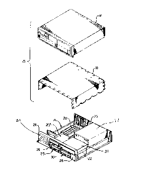
Figure 2 is an exploded perspective view of certain elements of the personal computer of
Figure l including a chassis, a cover, an electromechanical direct access storage device and a planar
board and illustrating certain relationships among those elements;
Figure 3 is a block diagram of certain components of the personal computer of Figures 1 and
2;
Figure 4 is a state diagram of the computer system of the present invention, showing the four
system states: normal, standby, suspend, and off;
Figure 5 is a block diagram showing the relevant portions of the power supply;
Figure 6 is an electrical schematic diagram of the hardware needed to accomplish the single
o switch suspend/resume functions of the present invention, showing the various interfaces to other
Flgures;
Figure 7 is a state diagram of one of the state machines of the programmable array logic
(PAL) device U2 shown in Figure 6;
Figure 8 is a flow chart showing generally the power-up routine of the present invention;
Figure 9 is a flow chart showing the details of the Supervisor Routine, which is called by the
APM approximately every second;
Figure 10 is a flow chart showing the details of the Suspend Routine of the present invention;
Figure 1 1 is a flow chart showing the details of the Boot-Up Routine of the present invention;
Figure 12 is a flow chart showing the details of the Resume Routine of the present invention;
Figure 13 is a flow chart showing the details of the Save CPU State Routine of the present
invention;
Figure 14 is a flow chart showing the details of the Restore CPU State Routine of the present
invention; and
Figure 15 is a flow chart showing the details of the Save 8959 State Routine of the present
2s invention.
Description of the Preferred Embodiment
While the present invention will be described more fully hereinafter with reference to the
CA 021200~ 1997-12-10
BC9-93-0 15 14
accompanying drawings, in which a preferred embodiment of the present invention is shown, it is
to be understood at the outset ofthe description which follows that persons of skill in the ~pl~pl;ate
arts may modify the invention here described while still achieving the favorable results of this
invention. Accordingly, the description which follows is to be understood as being a broad, teaching
disclosure directed to persons of skill in the appropriate arts, and not as limiting upon the present
invention. The present invention deals with the complete design of a computer system, including,
but not limited to computer architecture design, digital design, BIOS design, protected mode 80486
code design, application code design, operating system code design, and Advanced Power
Management advanced pro~ldllllllhlg interface usage. This application is written for those very
o f~miliar with all aspects of computer system design.
Referring now more particularly to the accompanying drawings, a microcomputer system embodying
the present invention is there shown and generally indicated at 10 (Figure 1). As mentioned
hereinabove, the computer 10 may have an associated monitor 11, keyboard 12, mouse 13, and
printer or plotter 14. The computer 10 has a cover 15 formed by a decorative outer member 16
(Figure 2) and an inner shield member 18 which cooperate with a chassis 19 in defining an enclosed,
shielded volume for receiving electrically powered data processing and storage components for
processing and storing digital data. At least certain of these components are mounted on a multilayer
planar 20 or motherboard which is mounted on the chassis 19 and provides a means for electrically
interconnecting the components of the computer 10 including those identified above and such other
associated elements as floppy disk drives, various forms of direct access storage devices, accessory
cards or boards, and the like. As pointed out more fully hereinafter, provisions are made in the planar
20 for the passage of input/output signals to and from the operating components of the
microcomputer.
The computer system has a power supply 17 and a power button 21, also hereinafter the switch 21.
Unlike in the usual power switch in a typical system, the power button 21 does not switch
unregulated line power to and from the power supply 17, as will be explained below. The chassis
CA 021200~ 1997-12-10
BC9-93-015 15
19 has a base indicated at 22, a front panel indicated at 24, and a rear panel indicated at 25 (Figure
2). The front panel 24 defines at least one open bay (and in the form illustrated, four bays) for
receiving a data storage device such as a disk drive for magnetic or optical disks, a tape backup
drive, or the like. In the illustrated form, a pair of upper bays 26, 28 and a pair of lower bays 29, 30
5 are provided. One of the upper bays 26 is adapted to receive peripheral drives of a first size (such
as those known as 3.5 inch drives) while the other 28 is adapted to receive drives of a selected one
of two sizes (such as 3.5 and 5.25 inch) and the lower bays are adapted to receive devices of only
one size (3.5 inch). One floppy disk drive is indicated at 27 in Figure 1, and is a removable medium
direct access storage device capable of receiving a diskette inserted thereinto and using the diskette
0 to receive, store and deliver data as is generally known. One hard disk drive is indicated at 31 and
is a fixed medium direct access storage device capable of storing and delivering data as is generally
known.
Prior to relating the above structure to the present invention, a summary of the operation in general
5 of the personal computer system 10 may merit review. Referring to Figure 3, there is shown a block
diagram of a personal computer system illustrating the various components of the computer system
such as the system 10 in accordance with the present invention, including components mounted on
the planar 20 and the connection of the planar to the I/O slots and other hardware of the personal
computer system. Connected to the planar is the system processor 40, also herein CPU 40, comprised
20 of a microprocessor, which is connected by a high speed CPU local bus 42 through a memory
control unit 46, which is further connected to a volatile random access memory (RAM) 53. The
memory control unit 46 is comprised of a memory controller 48, an address multiplexer 50, and a
data buffer 52. The memory control unit 46 is further connected to a random access memory 53 as
represented by the four RAM modules 54. The memory controller 48 includes the logic for mapping
25 addresses to and from the microprocessor 40 to particular areas of RAM 53. This logic is used to
reclaim RAM previously occupied by BIOS. Further generated by memory controller 48 is a ROM
select signal (ROMSEL), that is used to enable or disable ROM 88. While any applopliate
microprocessor can be used for system processor 40, one suitable microprocessor is the 80486 which
CA 021200~ 1997-12-10
BC9-93-015 16
is sold by INTEL. The Intel 80486 has an internal cache, therefore, any CPU 40 that is an Intel
80486 will have a CPU cache 41.
While the present invention is described hereinafter with particular reference to the system block
diagram of Figure 3, it is to be understood at the outset of the description which follows that it is
contemplated that the appal~lus and methods in accordance with the present invention may be used
with other hardware configurations of the planar board. For example, the system processor 40 could
be an Intel 80286 or 80386 microprocessor. As used herein, reference to an 80286 or 80386 or 80486
generally intends such a microprocessor as obtained from Intel. However, in recent times other
o manufacturers have developed microprocessors which are capable of executing the instruction set
of the Intel X86 architecture, and usage of the terms stated is intended to encompass any
microprocessor capable of executing that instruction set. As known to persons skilled in the
applicable arts, early personal computers typically used the then popular Intel 8088 or 8086
microprocessor as the system processor. These processors have the ability to address one megabyte
of memory. More recently, personal computers typically use the high speed Intel 80286, 80386, and
80486 microprocessors which can operate in a virtual or real mode to emulate the slower speed 8086
microprocessor or a protected mode which extends the addressing range from 1 megabyte to 4
Gigabytes for some models. In essence, the real mode feature of the 80286, 80386, and 80486
processors provide hardware compatibility with software written for the 8086 and 8088
microprocessors. Processors in the Intel family described are frequently identified by a three digit
reference to only the last three digits of the full type designator, as "486".
Retllrning now to Figure 3, the CPU local bus 42 (comprising data, address and control components)
provides for the connection of the microprocessor 40, a math coprocessor 44, a video controller 56,
2s a system cache memory 60, and a cache controller 62. The video controller 56 has associated with
it a monitor (or video display terminal) 57 and a video memory 58. Also coupled on the CPU local
bus 42 is a buffer 64 The buffer 64 is itself connected to a slower speed (compared to the CPU local
bus 42) system bus 66, also comprising address, data and control components. The system bus 66
CA 021200~ 1997-12-10
BC9-93-015 17
extends between the buffer 64 and a further buffer 68. The system bus 66 is further connected to a
bus control and timing unit 70 and a DMA unit 71. The DMA unit 71 is comprised of a central
arbiter 82 and a DMA controller 72. An additional buffer 74 provides an interface between the
system bus 66 and an optional feature bus such as the Industry Standard Architecture (ISA) bus 76.
Connected to the bus 76 are a plurality of I/O slots 78 for receiving ISA adapter cards (not shown).
ISA adapter cards are pluggably connected to the I/O slots 78 and may provide additional I/O
devices or memory for the system 10.
An arbitration control bus 80 couples the DMA controller 72 and central arbiter 82 to the I/O slots
0 78, a diskette adapter 84, and an Integrated Drive Electronics (IDE) fixed disk controller 86.
While the microcomputer system 10 is shown with a basic 4 megabyte RAM module 53, it is
understood that additional memory can be interconnected as represented in Figure 3 by the addition
of optional higher-density memory modules 54. For purposes of illustration only, the present
invention is described with reference to the basic four megabyte memory module.
A latch buffer 68 is coupled between the system bus 66 and a planar I/O bus 90. The planar I/O bus
90 includes address, data, and control components respectively. Coupled along the planar I/O bus
90 are a variety of I/O adapters and other components such as the diskette adapter 84, the IDE disk
adapter 86, an interrupt controller 92, an RS-232 adapter 94, nonvolatile CMOS RAM 96, also
herein referred to as NVRAM, a CMOS real-time clock 98, a parallel adapter 100, a plurality of
timers 102, the read only memory (ROM) 88, the 8042 104, and the power management circuitry
106. The 8042, shown at 104, is the slave microprocessor that interfaces with the keyboard 12 and
the mouse 13. The power management circuitry 106 is shown in Figure 6 and is more fully described
in the text accompanying Figures 6 and 7. The read only memory 88 includes the BIOS that is used
to interface between the I/O devices and the operating system of the microprocessor 40. BIOS stored
in ROM 88 can be copied into RAM 53 to decrease the execution time of BIOS. ROM 88 is further
responsive (via ROMSEL signal) to memory controller 48. If ROM 88 is enabled by memory
CA 021200~ 1997-12-10
BC9-93-015 18
controller 48, BIOS is executed out of ROM. If ROM 88 is disabled by memory controller 48, ROM
is not responsive to address inquiries from the microprocessor 40 (i.e. BIOS is executed out of
RAM).
s The real-time clock 98 is used for time of day calculations and the NVRAM 96 is used to store
system configuration data. That is, the NVRAM 96 will contain values which describe the present
configuration of the system. For example, NVRAM 96 contains information describing the capacity
of a fixed disk or diskette, the type of display, the amount of memory, time, date, etc. Of particular
importance NVRAM will contain data (can be one bit) which is used by memory controller 48 to
0 determine whether BIOS is run out of ROM or RAM and whether to reclaim RAM intended to be
used by BIOS RAM. Furtherrnore, these data are stored in NVRAM whenever a special
configuration program, such as SET Configuration, is executed. The purpose of the SET
Configuration program is to store values characterizing the configuration of the system to NVRAM.
Nearly all of the above devices comprise volatile registers. To prevent the unnecessary cluttering
of the drawings, the registers of a particular device will be referenced to that device. For example,
the CPU registers will be referred to as the CPU 40 registers and the video controller registers will
be referenced as the video controller 56 registers.
As mentioned hereinabove, the computer has a cover indicated generally at 15 which cooperates with
the chassis 19 in forming an enclosed, shielded volume for cont~ining the above identified
components of the microcomputer. The cover 15 preferably is formed with an outer decorative cover
member 16 which is a unitary molded component made of a moldable synthetic material and a
2s metallic thin sheet liner 18 formed to conform to the configuration of the decorative cover member.
However, the cover can be made in other known ways and the utility of this invention is not limited
to enclosures of the type described.
CA 021200~ 1997-12-10
BC9-93-015 19
States of Operation
Referring now to Figure 4, a state diagram of the computer system of the present invention is shown.
The computer system 10 ofthe present invention has four states: a normal operating state 150, a
standby state 152, a suspend state 154, and an off state 156. The transitions between the states
5 shown in Figure 4 are meant to be descriptive of the preferred embodiment, but not limiting.
Consequently, additional events may alternatively be used to cause state transitions.
The normal operating state 150 of the computer system 10 of the present invention is virtually
identical to the normal operating state of any typical desktop computer. Users may use applications
0 and basically treat the computer as any other. One difference, transparent to the user, is the presence
of a power management driver in the operating system (the "APM OS driver"), which runs in the
background, and various APM BIOS routines. The APM BIOS routines are discussed in the text
below and include the Suspend Routine, the Resume Routine, the Boot-Up Routine, the Supervisor
Routine, the Save CPU State Routine, and the Restore CPU State Routine. One APM BIOS routine
5 not shown on any of the Figures is the APM BIOS Routing Routine. The APM BIOS Routing
Routine essentially accepts commands from the APM OS driver and calls the applopliate APM
BIOS routine. For example, when the APM OS driver issues the Suspend Comm~n(l, the APM BIOS
Routing Routine calls the Suspend Routine. AS another example, whenever the APM OS driver
issues the Get Event command, the APM BIOS Routing Routine calls the Supervisor Routine. These
20 routines are located in BIOS and are shadowed when the BIOS is shadowed. The power management
driver in the OS and the APM BIOS routines control the computer's transition between the four
states. A reference to the word "APM" by itself generally is a reference to the APM OS driver,
although the context may dictate otherwise.
25 The second state, the standby state 152, uses less electrical power than the normal operating state
150, yet leaves any applications executing as they would otherwise execute. In general power is
saved in the standby state 152 by the code placing devices into respective low power modes. In the
preferred embodiment, electrical power is conserved in the standby state 152 by ceasing the
CA 021200~ 1997-12-10
BC9-93-015 20
revolutions of the fixed disk (not shown) within the fixed disk storage device 31 and by ceasing
generating the video signal, as will be more fully explained below. However, this is not intended
to be limiting and other methods may be used to reduce power consumption, such as slowing or
stopping the CPU clock.
s
In the preferred embodiment, electrical power is conserved in two separate ways. First, in the
normal operating state 150, the fixed disk within the fixed disk storage device 31 is constantly
spinning at typically 3600 revolutions per minute (RPM). In the standby state 152, the IDE disk
controller 86 is given the command to cause the fixed disk storage device 31 to enter a low-power
o mode (the fixed disk inside the fixed disk storage device 31 ceases spinning), thereby conserving the
power the motor (not shown) inside the fixed disk storage device 31 typically consumes while
spinning the fixed disk.
Second, in the normal operating state 150, the video controller 56 of the computer system constantly
5 generates a video signal (HSYNC, VSYNC, R, G, B, etc. as is well known in the art) corresponding
to the image seen on the video display terminal 57. In the standby state 152 the video controller 56
ceases generating the video signal, thereby conserving the electrical power normally consumed by
the video controller 56. HSYNC, VSYNC, R, G, and B are all driven to approximately 0.00 VDC.
Using a VESA (Video Electronics Standards Association) compliant monitor allows further power
20 savings because VESA compliant monitors turn themselves off when HSYNC and VSYNC are at
approximately 0.00 VDC.
Note that some systems have "screen-savers," which cause the screen 57 to become dark to prevent
phosphor burn-in of the front surface of the video display terminal. In most of such systems, the
25 video controller 56 is still generating a video signal; it is merely generating a video signal
corresponding to a dark screen or a dynamic display. Thus, a computer system executing a screen-
saver still consumes the electrical power necessary to generate the video signal.
CA 021200~ 1997-12-10
BC9-93-015 21
The third state is the suspend state 154. In the suspend state 154, computer system consumes an
extremely small amount of electrical power. The suspended computer consumes less than 5 watts
of electrical power from the wall outlet in the preferred embodiment. The only power consumed is
a slight trickle of power used to monitor the switch 21 either from the AUX5 output from the power
supply 17, or from a battery 171 inside the computer system, as will be explained more fully below
in the text accompanying Figure 5.
This small use of electrical power is accomplished by saving the state of the computer system to the
fixed disk storage device (the hard drive) 31 prior to turning the power supply "off." To enter the
0 suspend state 154, the CPU 40 interrupts any applications and transfers program execution control
of the CPU to the power management driver. The power management driver ascertains the state of
the computer system 10 and writes the entire state of the computer system to the fixed disk storage
device 31. The state ofthe CPU 40 registers, the CPU cache 41, the system RAM 53, the system
cache 60, the video controller 56 registers, the video memory 56, and the rem~ining volatile registers
are all written to the fixed disk drive 31. The entire state of the system 10 is saved in such a way that
it can be restored without significant usability penalties. That is, the user need not wait for the
system to load the operating system, and load the graphical user interface as it normally would.
The computer then writes data to the non-volatile CMOS memory 96 indicating that the system was
suspended. Lastly, the CPU 40 causes the power supply 17 to stop providing regulated power. The
computer system 10 is now powered down with the entire state of the computer safely saved to the
fixed disk storage device 31.
The word "state" is used throughout this document in two similar, but possibly confusing ways.
2s Devices can be "in" a particular state. The four system states--normal 150, standby 152, suspend 154,
and off 156--refer to the general state of the computer system 10 of the present invention. These
"states" describe the computer system 10 in a general way. For example, while in the normal
operating state 150, the CPU 40 is still executing code and changing a plurality of registers within
CA 021200~ 1997-12-10
BC9-93-0 15 22
the system 10. Likewise, similar activity occurs while in the standby state 152. Thus, the memory
and register configuration of the computer system 10 is dynamic while the system 10 is in the normal
operating state 150 and the standby state 152.
5 Other devices can also be "in" certain states. The programmable logic array U2 can be in several
states, as will be explained in the text accompanying Figure 7.
Contrast the above with the "state of ~' a device, for example, the "state of the computer system 10"
or the "state of the CPU 40." The "state of~' a device refers to the condition of that device at a
0 particular computer cycle. All memory locations and registers will have particular binary values. The
"state oft' a device is a static binary snapshot of the contents of that device.
The "state of~' the computer system 10 refers to operational equivalents and not necessarily exact
copies. For example, a computer system in a state A may have certain memory in either CPU cache
S 41 or system cache 60. It is possible to "flush" the contents of either cache back to the system RAM
53, putting the computer system in a state B. Purely speaking, the state of the computer system in
state A is different from the state of the computer system in state B, because the contents of cache
and system RAM are different. However, from a software operational perspective, state A and state
B are the same, because, aside from a slight decrease in system speed (caused by the program not
20 having the benefit of executing out of cache), the executing programs are not affected. That is, a
computer in state A and a computer in state B are software operationally equivalent, even though
the computer whose cache was flushed will experience a slight decrease in performance until the
cache areas are reloaded with helpful code.
25 The word "power" is also used in two similar, but possibly confusing ways. "Power" most often
refers to electrical power. However, "power" also refers to computational power occasionally. The
context should make the intended usage obvious.
CA 021200~ 1997-12-10
BC9-93-015 23
A "circuit" is generally a reference to a physical electronic device or a plurality of devices
electrically interconnected. However, the term "circuit" also is intended to encompass CPU code
equivalents of physical electronic devices. For example, on the one hand, a two-input NAND gate
can be implemented via a 74LS00 or, equivalently, in a programmable device. These two devices
are physical electronic devices. On the other hand a NAND gate can also be implemented by having
the CPU 40 read two inputs from two CPU-readable input ports, generate the NAND result using
a CPU command, and output the result via a CPU-writable output port. These CPU-interfacable ports
can be simple, such as decoded latches, or their programmable device equivalent, or complex, such
as PIAs, which are well-known in the art. "Circuit" is meant to include all three examples of NAND
0 gate implementations. In some cases, "circuit" may refer to merely an electrical pathway. Types of
electrical pathways include a wire, a trace or via on a printed circuit board, etc., or any combination
of types of electrical pathways that form a single electrically connected pathway.
A "signal" may refer to a single electrical waveform or a plurality of waveforms. For example, the
video controller generates a video signal. The video signal is actually a plurality of signals on a
plurality of electrical conductors: HSYNC, VSYNC, R, G, B, etc. as is well known in the art.
Returning now to Figure 4, the fourth and final state is the off state 156. The off state 156 is virtually
identical to any typical computer system that has been turned offin the ordinary sense. In this state,
the primary/regulation unit 172 of the power supply 17 ceases providing regulated power to the
computer system 10, (with the exception of a slight trickle of regulated power through AUX5, as will
be more fully explained in the text accompanying Figure 5) but the state of the computer system 10
has not been saved to the fixed disk 31. The suspend state 154 and the off state 156 are similar in that
the power supply 17 no longer generates regulated power. They differ in that in the off state 156, the
state of the computer system 10 is not saved to the hard drive 31, as it is in the suspend state 154.
Moreover, when leaving the off state 156, the computer 10 "boots" as if it is being turned on. That
is, any executing code must be started either by the user or automatically by a means such as the
AUTOEXEC.BAT file. However, when leaving the suspend state 154, the computer 10 resumes
CA 021200~ 1997-12-10
BC9-93-0 15 24
executing where it was when it was interrupted.
Figure 4 also shows a general overview of the events that cause transitions between the four states.
These events will be further explained in the text accompanying Figures 6 through 8; however, a
s cursory explanation may be helpful. The power button 21, two timers (the inactivity standby timer
and the inactivity suspend timer, see Figure 9 and accompanying text), and an enter suspend flag (see
Figures 6 and 7 and accompanying text) all of which affect which state the computer enters. In
general, the two timers can be either hardware or CPU code timers, executing on the CPU as a
program. In the pleft;lled embodiment, they are both CPU code timers, executing from the BIOS
0 data segments. However, the two timers could conceivably be hardware timers, which would be a
better solution, in that it would reduce the overhead of the system. The timers are more fully
explained in the text accompanying Figure 9. Both timers are active when the computer 10 is in
either the normal operating state 150 or the standby state 152. The timers are in communication with
other routines such that the expiration of either timer causes a transition as outlined below. Either
5 or both timers can be configured to expire after a certain period of time, depending on the particular
needs of the user. In the preferred embodiment, the inactivity standby timer and the inactivity
suspend timer can be set to expire after 15 to 90 minutes. Either or both timers can be stopped, that
is, configured to never expire. "Stopping" the timers can take the form of actually ceasing the
incremental counting action of the timers or merely ignoring their expiration. In the preferred
20 embodiment, setting a zero value in the timer expiration value causes the timer expiration not to be
tested. The user of a networked computer may, for example, not want the computer to enter the
suspend state 154 because doing so may cause the LAN to fail with respect to that computer.
In theory, the timers can count up or count down and can be reset to a fixed predetermined state and
2s expected to count to another fixed predetermined state when the timer is started (or restarted) or the
present value can be used and a difference or sum calculated as the endpoint expiration trigger. In
the preferred embodiment, when the timers are reset, the present value of the minutes variable from
the real-time clock 98 is stored. The timers are checked for expiration by subtracting the current
CA 021200~ 1997-12-10
BC9-93-015 2s
minutes value from the saved minutes value and comparing the difference to the values selected by
the user.
Both timers are affected by certain system activity. For example, in the preferred embodiment, user
activity in the form of keyboard 12 keys being pressed, the mouse 13 being moved, mouse 13
buttons being pressed, or hard drive 31 activity causes each timer to be restarted, as more fully
explained in the text accompanying Figure 9; therefore, while a user is pressing keyboard 12 keys
or using the mouse 13, neither timer will expire. In addition other system events might be used to
reset the timers. Any of the hardware interrupts might alternatively be monitored for activity. Thus,
o it might be desirable to have printing prevent the system from entering the suspend state 154.
The enter suspend flag is a CPU-manipulable and readable latch within the programmable logic
array U2, which will be more fully explained in the text accompanying Figure 7. In short, putting
the programmable logic array U2 in one mode causes a press of the switch 21 to place the system
10 into the off state 156 and putting the programmable logic array U2 into another mode causes a
press of the switch 21 to place the system 10 into the suspend state 154. If the computer system 10
is in the normal operating state 150 and the power button 21 is pressed while the enter suspend flag
written to the programmable logic array U2 is ~~2~ then the computer system 10 enters the off state
156, as shown at 158. If the computer system 10 is off state 156 and the power button 21 is pressed,
then the computer system enters the normal operating state.
If the computer system 10 is in the normal operating state 150, one event can cause the computer to
enter the standby state 152: if the inactivity standby timer expires, the computer system 10 will
change to the standby state 152, as shown at 162. While in the standby state 152, any system activity
2s of the kind previously described will cause the computer l O to leave the standby state 152 and re-
enter the normal operating state 150, as shown at 164.
If the computer 10 is in the normal operating state 150, two events can cause it to enter the suspend
CA 021200~ 1997-12-10
BC9-93-015 26
state 154. First, if the inactivity suspend timer expires, the computer system 10 will change to the
suspend state 154, as shown at 166. Second, the user can cause the computer 10 to enter the suspend
state 154 immediately by pressing the power button 21 while the enter suspend flag written to the
programmable logic array U2 is 012, also shown at 166. While in the suspend state 154, the user
s changes to the normal operating state 150 by pressing the power button 21, as shown at 168.
In addition, several external events alternatively may be used to change the system 10 from the
suspend state 154 to the normal operating state 150, at 168. For example, a telephone ring detect
circuit could be added to the circuitry of Figure 6 and configured to cause the system 10 to leave the
0 suspend state 154 and enter the normal operating state 150 when an attached telephone line rings.
Such a modification might be useful for a system receiving telefax data or digital data. The system
would only consume power when receiving incoming information. Likewise an interface between
the real-time clock and Figure 6 could alternatively allow an alarm-type event to cause the system
10 to leave the suspend state 154 and enter the normal operating state 150. Such a system might be
s useful in sending telefax or digital data at a certain time of day to take advantage of lower telephone
usage rates.
Lastly, if the computer system 10 is in the standby state 152 and the inactivity suspend timer expires,
then the computer 10 changes to the suspend state 154 as shown at 170. The computer system 10
cannot change back from the suspend state 154 to the standby state 152, but may only transition to
the normal operating state 150 as described in the text accompanying transition 168.
Obviously, the computer system 10 cannot instantaneously change states. In each transition from one
of the four states, a certain period of time will be required to make the necessary system changes.
2s The details of each transition period will be explained in the text accompanying Figures 6 through
15.
System Hardware
CA 021200~ 1997-12-10
BC9-93-015 27
Before discussing the details of the code executing on the CPU 40, it may be helpful f1rst to discuss
the hardware required to achieve the four states. A block diagram of the power supply 17 is shown
in Figure 5. The power supply 17 has two units: a control unit 174 and a primary/regulation unit
172. The power supply 17 has several inputs: Line-In, which accepts 115 VAC from a typical wall
s outlet, and ON, which controls the regulation activity of the power supply 17. The power supply 17
has several outputs: AC Line-Out,15 VDC, ~12 VDC, AUX5, GND, and POWERGOOD. The AC
Line-Out is unregulated 115 VAC that is typically passed to the electrical power input (not shown)
of the video display terminal 57. The control unit 174 accepts the ON input and generates the
POWERGOOD output. The primary/regulation unit 172 selectively regulates the 115 VAC from the
0 Line-In input down to ~5 VDC, ~12 VDC. Whether the primary/regulation unit 172 regulates power
depends on the value of ON, as interfaced by the control unit 174. In the preferred embodiment, the
control unit 174 should provide isolation for the circuitry generating the ON signal, for example, an
appropriate optoisolator.
The Line-In input and the AC Line-Out, ~t5 VDC, +12 VDC, GND, and POWERGOOD outputs are
well known in the art. When the power supply 17 is "off," that is, not providing regulated voltages
from the Line-In, the POWERGOOD signal is a logical ZERO. When the power supply 17 is "on,"
the power supply 17 generates the ~5 VDC and ~12 VDC regulated voltages from the 115 VAC
Line-In. These four regulated voltages and their associated GND are the "system power" as is
commonly known in the art. When the regulated voltages attain levels within acceptable tolerances,
the POWERGOOD signal changes to a logical ONE.
The AUX5 output provides an auxiliary +5 VDC to the planar. When the power supply 17 is plugged
into a typical wall outlet supplying a nominal 115 VAC, the primary/regulation unit 172 provides
regulated +5 VDC at AUX5, whether the power supply is "on" or "off." Thus, while plugged in, the
power supply 17 is always providing a nominal +5 VDC at AUX5. The AUX5 output differs from
the +5 output in that the primary/regulation unit 172 only generates regulated +5 VDC through the
+5 output while the power supply 17 is "on." The AUX5 output further differs from the +5 output
CA 021200~ 1997-12-10
BC9-93-015 28
in that in the preferred embodiment, the primary/regulation unit 172 supplies several amps of current
at +5 VDC through the +5 output, while the primary/regulation unit 172 supplies less than an amp
at +S VDC though the AUX5 output.
s Typical prior power supplies use a high-amperage double-throw switch to connect and disconnect
the Line-In input to and from the regulation section of the power supply. The power supply 17 in the
present invention does not use a high-amperage double-throw switch. Rather, the switch 21 controls
circuitry that generates the ON signal. In the preferred embodiment, the switch 21 is a momentary
single pole, single throw pushbutton switch; however, those skilled in the art could adapt the
0 circuitry of Figure 6 to make use of other types of switches such as a single-pole, double throw
switch. The AC Line-In is always connected to the primary/regulation unit 172 from the wall outlet.
When ON is a logical ONE (approximately AUX5, nominally +5 VDC), the primary/regulation unit
172 does not regulate the 115 VAC Line-In to ~5 VDC or ~12 VDC through the ~5 or ~12 outputs.
The primary/regulation unit 172 merely provides a low-amperage nominal +5 VDC at the AUX5
output. On the other hand, when ON is a logical ZERO (approximately GND), the
primary/regulation unit 172 does regulate the 115 VAC Line-In to ~5 VDC and ~12 VDC through
the four ~5 and ~ 12 outputs, respectively. Thus, when ON is a ONE, the power supply 17 is "off '
and when ON is a ZERO, the power supply 17 is "on."
If specified, power supplies having an AUX5 output and an ON input, like the power supply 17
described above, can be obtained from suppliers of more conventional power supplies.
Referring now to Figure 6, a schematic drawing of the electronic circuitry of the computer system
10 of the present invention is shown. The circuitry in Figure 6 is responsible for interfacing between
2s the switch 21, the power supply 17, the video display terminal 57, and code executing on the CPU
40.
The circuitry comprises three (3) integrated circuits: Ul, a f1rst preprogrammed PAL16L8; U2, a
CA 021200~ 1997-12-10
BC9-93-0 15 29
second preprogrammed PALl6L8; and U3, a 74HCl32, which is well known in the art. In general,
the PALs U1 and U2 interface between the planar I/O bus 90 of Figure 3 and the rem~ining circuitry
of Figure 6. The circuitry further comprises the switch 21, ten resistors Rl-R10, five capacitors Cl-
C5, four N-type MOSFETs Q l -Q4, which are standard low-current NMOS FETs suitable for acting
s as a logic switch in the preferred embodiment, and a dual diode package CRl, which is a standard
low-current diode package, all configured and connected as shown in Figure 6. The resistors Rl-R10
are 1/4 Watt resistors and are of values shown in Figure 6, + 5%. The capacitors C1-C2 are
electrolytic capacitors of the values shown in Figure 6, ~t 10%. The capacitors C3-C5 are 0.1 ,uF (~
10%) ceramic capacitors.
The first PAL U1 is connected to address lines SA(1) through SA(15) and the AEN (address enable)
line. SA(l) through SA(15) and AEN are part of the planar I/O bus 90 shown in Figure 3. The first
PAL U1 is programmed to be merely an address decoder, presenting an active low signal
PM_PORT_DCD# when a predetermined address is presented on address lines SA(1) through
5 SA(15) and the AEN (address enable) line is active.
The second PAL U2 is programmed to provide a readable byte and three writable bits in the lower
three bits of the I/O port mentioned above, also herein referred to as the "power management port."
The second PAL U2 has eight (8) inputs from the planar I/O bus 90: SD(0), SD(1), SD(2), SA(0),
20 IOW#, IOR#, RESETDRV, and IRQ(1). The second PAL U2 is reset to a known initial condition
by the active high signal RESETDRV input at pin 2, which is generated by the memory controller
46, as is well known in the art. The second PAL U2 is more fully described in the text accompanying
Figure 7 and Tables I and II.
2s The third device has two portions, here identified as U3A and U3B, which form an SR latch, also
known as a NAND latch, which is well known in the art. The SR latch has pins l and 5 of U3 as
inputs (pin 1 is the SET input and pin 5 is the RESET input) and pin 3 of U3A as the output. While
both inputs are a logical ONE, the output retains its latched output value. If SET is placed to a
CA 021200~ 1997-12-10
BC9-93-015 30
logical ZERO, the output becomes a logical ONE. If the SET input is returned to a logical ONE, the
output is latched at a logical ONE. If the RESET input is placed to a logical ZERO, the output
becomes a logical ZERO. If the RESET input is returned to a logical ONE, the output is latched at
a logical ZERO.
s
If the POWERGOOD signal is a logical ONE, which indicates that the regulated voltages are at
proper levels, then a third portion of the third device, here identified as U3C, acts as an inverter for
the pin 12 output ofthe second PAL U2. If the POWERGOOD signal is a logical ZERO, indicating
that VCC is either floating near ground or ramping up to or ramping down from +5 VDC, then the
10 output at pin 8 of the third portion of the third device U3C remains a logical ONE, preventing any
noise from pin 12 of the second PAL U2 from affecting the SR latch created by the first and second
portions U3A and U3B of the third device.
The switch 21 connects to the circuitry of Figure 6 at JP 1. A resistor/capacitor subcircuit R2 and C l
15 debounce a closure event of the switch 21. The fourth portion of the third device U3D is configured
as an inverter with pin 12 being pulled to VBAT (approximately +4.3 VDC when AUX5 is a
nominal +5 VDC) through R6, which inverts the debounced switch closure. A current-limiting
resistor R10 protects pin 1 1 of the fourth portion of the third device U3D from any current that may
flow from pin 8 of the second PAL U2 when that device powers up or down.
The SR latch should never power off. However, if it does, R7 and C3 are designed to place the SR
latch into a state on power-up such that the power supply 17 will be in the "off" state when the SR
latch is repowered.
Resistors Rl, R3, R4, R5, R6, R8 and R9 are pull-up resistors, pulling their respective lines to either
VCC, VBAT, or AUX5. Transistors Q1, Q2, Q3, and Q4 are inverters. R4 and C2 form an RC pair
causing C2 to charge until it reaches VCC. Transistor Q5 drains transistor C2 when the pin 19
output of the second PAL U2 is a logical ONE. When the voltage stored in C2 is below
CA 021200~ 1997-12-10
BC9-93-015 31
approximately +2.7 VDC, Q1 does not conduct and R3 pulls the pin 11 input ofthe second PAL U2
to VCC, making it a logical ONE. If C2 charges to approximately +2.7 VDC or greater, then Q1
conducts, pulling the pin 11 input to GND, making it a logical ZERO.
When the pin 18 output of the second PAL U2 is a logical ZERO, R8 and R9 pull the BLNK# and
ESYNC lines, respectively, to VCC. With the ESYNC and BLNK# lines at VCC, the video
controller 56 generates a video signal. When the pin 18 output of the second PAL U2 is a logical
ONE, transistors Q2 and Q3 conduct, pulling BLNK# and ESYNC, respectively, to GND, causing
the video controller 56 to cease generating the video signal.
The electronic circuitry shown in Figure 6 has three power sources: VCC, AUX5, and VBAT. VCC
and AUX5 are generated by the power supply 17 and are nominally +5.0 VDC. VCC and its
associated GND return line enter through the main power connector (not shown) on the planar 20
as is well known in the art. AUX5 is connected to the circuitry at pin 1 of JP2. The AUX5 return
enters and is connected to the GND line at pin 3 of JP2. VBAT is the power output of the battery 171
and is nominally 3.5 VDC. The battery 171 is a lithium battery and is well known in the art.
The PALs U1 and U2 have their VCC input at pin 20 connected to VCC. In addition, several
resistors R3, R4, R8, and R9 are also connected to VCC. The power supply 17 only provides
regulated +5 VDC when the power supply is "on" and plugged into a typical wall outlet supplying
a nominal 115 VAC, as is well known in the art. Thus, when the power supply is either "off~' or
unplugged, the PALs U1 and U2 and resistors R3, R4, R8, and R9 are not receiving +5 VDC.
On the other hand, whenever the power supply 17 is plugged into a typical wall outlet supplying a
nominal 115 VAC, the power supply 17 provides regulated +5 VDC at AUX5, whether "on" or
"off." Thus, those devices connected to AUX5 receive +5 VDC whenever the power supply 17 is
plugged in.
CA 021200~ 1997-12-10
BC9-93-015 32
Moreover, U3 and the resistors R1, R2, and R6 are always receiving electrical power, because the
diodes of CR1 interface VBAT and AUX5 in such a way that devices attached to VBAT are always
receiving power. While plugged into a typical wall outlet, the power supply 17 provides +5 VDC
at AUX5 and the devices attached to VBAT (U3 and the resistors Rl, R2, and R6) receive
s approximately +4.3 VDC (+5 VDC of AUX5 minus the diode drop of the diode within CR1 between
AUX5 and VBAT). When not plugged in, the power supply 17 ceases providing regulated power
to the AUX5 line and U3 and the resistors R1, R2, and R6 receive power *om VBAT. A typical
74HC132 requires a minimum DC supply voltage of +2.0 VDC. Thus, as long as VBAT retains a
sufficient charge to provide +2.0 VDC, U3 is sufficiently powered.
The circuitry of Figure 6 can have numerous alternative modifications and still come within this
invention. For example, the real-time clock 98 can be electrically connected to the Figure 6 circuitry
and configured to be diode ORed to the ON# signal such that at a specific time of day, the computer
system 10 is changed *om the suspend state 154 to the normal operating state 150. Likewise a
5 telephone ring-detect circuit could alternatively be added to the Figure 6 circuitry and configured
to be diode Ored to the ON# signal such that a ring of an attached telephone line would cause the
system 10 to leave the suspend state 154 and enter the normal operating state 150.
Referring back to Figure 6, the second PAL U2 has two state machines. A state diagram of one of
20 the state machines in the second PAL U2 is shown in Figure 7. Table I and Table II describe the
other state machine and certain miscellaneous aspects of the second PAL U2.
Figure 7 shows one of the state machines within the second PAL U2. TE1 and TE0 together allow
four states: switch state ~~2 176, switch state 0 12 178, switch state 112 180, and switch state 1 ~2 182.
TE1 and TE0 are not directly writable to the second PAL U2, rather, states change in response to
closure events of the switch 21 and other events, such as resetting of the computer system 10. With
system power not being provided by the power supply 17, the second PAL U2 is not being powered
CA 021200~ 1997-12-10
BC9-93-015 33
and, therefore, its state is meaningless, at 174. A press of the switch 21 and other events (such as a
telephone ring detector causing the power supply 17 to provide system power) cause the power
supply 17 to begin providing system power, as described in the text accompanying Figure 6. When
the switch 21 pressed or the RESETDRV signal is active, the second PAL U2 enters switch state ~~2
s 176. Releasing the switch 21 or the RESETDRV becoming inactive while the switch 21 is not
pressed causes the second PAL U2 to enter switch state 012 178. Pressing the switch 21 again causes
the second PAL U2 to enter switch state 112 180. Releasing the switch 21 again causes the second
PAL U2 to enter switch state 102 182. Subsequent closures of switch 21 causes the second PAL U2
to cycle through the four states, as shown in Figure 7. The second PAL U2 is in switch state 012 178
o when the computer system 10 is in the normal operating state 150.
Switch state 012 178 is the switch state corresponding to the normal on state for the TE1, TEO state
machine. Application programs will execute while in that state. The system 10 may enter and leave
the standby state 152 in that state. Switch state 012 178 also corresponds to a user-generated suspend
abort request. Switch state 102 is the switch state corresponding to a suspend request by the user.
That is, starting with the system in the offstate 156, pressing the switch 21 once places the computer
system in the normal operating state 150. Pressing the switch 21 once again generates a suspend
request (OFFH at the power management port), which is read by the Supervisor Routine, which is
discussed more fully in the text accompanying Figure 9. Pressing the switch 21 a third time, before
the system 10 is in the suspend state 154, generates a suspend abort request (OFEH at the power
management port), which is read by the Suspend Routine.
Table I adds several comments to the four states of Figure 7. While in switch states ~~2 176, 012 178,
and 1 12 180, the power management port outputs OFFH in response to a read. On the
2s
TE 1 TEO Comments
O O Clears the display blanking bit
Read of power management port = OFFH
CA 021200~ 1997-12-10
BC9-93-015 34
O 1 Display blanking bit controlled by SD(2)
Read of power management port = OFFH
Display blanking bit controlled by SD(2)
s Read of power management port = OFFH
0 Sets the display blanking bit
Read of power management port = OFEH
TABLE I
other hand, while in switch state 102 182, the power management port outputs OFEH in response to
a read. A press and release of switch 21 causes the second PAL U2 to leave switch state 012 and
enter switch state 102 182, which signals a hardware suspend request. The Supervisor Routine
becomes aware of the hardware suspend request by reading the power management port. A OFEH
in response to a read indicates a hardware suspend request.
The TE1, TEO state machine also affects the video blanking circuitry. While in switch state ~~2 176,
the display blanking bit is cleared, causing the video controller 56 to generate the video signal. While
in switch state 102 182, the display blanking bit is set, causing the video controller 56 to stop
generating the video signal. While in switch states 012 178 and 112 180, the display blanking bit is
controlled by writes to D2, as explained below.
2s Table II shows the other state machine of the second PAL U2 and shows how writes to SD2 affect
the video signal.
S2 S 1 SO Comments
X O O While in switch state 102, turns '-offl' the power supply
immediately
X O 1 While in switch state 102, starts failsafe timer (C2 charges)
CA 021200~ 1997-12-10
BC9-93-015 35
X 1 0 Turns "off" powersupplyimmediately
X 1 1 Resets failsafetimer(C2 drained)
s 0 X XTurns onvideo signal
X X Turns off video signal
TABLE II
The U2 circuitry within the PAL provides for three bits--SD(0), SD(l), SD(2)--at the power
management port. The three bits are labeled S0, S 1, and S2 in Table II. SD(2) controls the video
blanking by controlling the pin 18 DISPLAY_OFF output of the second PAL U2. Writing a ONE
5 to the SD(2) bit of the power management port turns off the video signal by causing the pin 18
DISPLAY_OFF output to assert a logical ONE, causing transistors Q2 and Q3 to conduct, pulling
BLNK# and ESYNC to GND, which causes the video controller 56 to cease generating the video
signal. Likewise, writing a ZERO to SD(2) of the power management port causes pin 18
DISPLAY_OFF output to assert a logical ZERO, causing transistors Q2 and Q3 to stop conducting,
20 allowing resistors R8 and R9 to pull BLNK# and ESYNC to VCC, which allows the video controller
56 to generate the video signal.
The IRQ(l) input also controls the video blanking. IRQ(l) is the keyboard hardware interrupt;
pressing a key on the keyboard 12 causes IRQ(l) to pulse. A pulse on IRQ(l) while the video signal
25 is off immediately turns the video signal back on by causing the pin 18 DISPLAY_OFF output to
assert a logical ZERO, causing transistors Q2 and Q3 to stop conducting, allowing resistors R8 and
R9 to pull BLNK# and ESYNC to VCC, which allows the video controller 56 to generate the video
signal. Using IRQ(l) in this manner gives the user immediate feedback in the form of a restored
video display when retllrning from the standby state 152 to the normal operating state 154. Without
30 it, the user might not receive feedback until possibly seconds later when the APM checks for user
activity, as explained in the text accompanying Figure 9.
CA 021200~ 1997-12-10
BC9-93-0 15 36
SD(l) and SD(0) work in tandem to provide four operating states: ~~2~ 012, 102, and 112. The second
PAL U2 is initialized by the RESETDRV input to the ~~2 state. In addition, while in any of the four
states, writing a XXXXXXO02 to the power management port places the second PAL U2 in the ~~2
state. In the ~~2 state, the switch 21 acts like the power switch of typical power supplies, described
5 in the text accompanying Figure 5. Pressing the switch 21 while in the ~~2 state turns "off" the
power supply 17 by causing the pin 12 output of the second PAL U2 to assert a logical ONE, causing
the output pin 3 of the SR latch to latch into a logical ZERO state, allowing ON to be pulled HIGH
by R6, causing the primary/regulation unit 172 of the power supply 17 to stop providing regulated
voltages along the ~5 and ~12 lines. In this state, the APM is disconnected as is more fully explained
0 in the System Software discussion, below. Reading the power management port while in the ~~2 state
causes the circuitry to return OFEH. In the preferred embodiment, this byte is read and tested to
ensure that the hardware is present.
While in any of the four states, writing a XXXXXX0 12 to the power management port causes the
second PAL U2 to enter the 012 state. The 012 state is the normal APM state. Reading the power
management port immediately after entering the 012 state, before the switch 21 is pressed, causes
the circuitry to return OFFH. Pressing and releasing the switch 21 while in the 012 state causes two
events: (1) the value returned from a read of the power management port toggles between OFEH and
OFFH and (2) the value asserted at pin 18 toggles, causing the video controller 56 to toggle the video
20 signal on and off with each press. Moreover, the first time the switch 21 is pressed, failsafe timer
starts by causing the pin 19 TRIGGER# output to assert a logical ZERO, causing Q5 to stop
conducting, allowing the capacitor C2 to start charging. When the voltage stored in C2 is below
approximately +2.7 VDC, Q 1 does not conduct and R3 pulls the pin 1 1 input of the second PAL U2
to VCC, making it a logical ONE. If C2 charges to approximately +2.7 VDC or greater, then Ql
25 conducts, pulling the pin 11 input to GND, making it a logical ZERO. Whenever the pin 11
DELAY_IN# is a logical ZERO, then the second PAL U2 turns "off" the power supply 17 by
causing the pin 12 output of the second PAL U2 to assert a logical ONE, causing the output pin 3
of the SR latch to latch into a logical ZERO state, allowing ON to be pulled HIGH by R6, causing
CA 021200~ 1997-12-10
BC9-93-015 37
the primary/regulation unit 172 of the power supply 17 to stop providing regulated voltages along
the ~5 and ~12 lines. Repeated switch closures cause the failsafe timer to toggle on and off.
Thus, while in the 012 state, before the switch is pressed, the value returned from a read is OFFH and
s the video signal is being generated; the first time the switch 21 is pressed, the value returned from
a read changes to OFEH and the video signal stops being generated, causing the video display
tf nnin~l 57 to blank. A second press of the switch 21 causes the value returned from a read to change
back to OFFH and the video controller 56 starts generating the video signal again. The toggling
nature causes repeated pressing of the switch 21 to behave such that an odd total number of switch
lO presses results in a value of OFEH and a blanked video signal and an even total number of switch
presses results in a value of OFFH and a generated video signal.
While in any of the four states, writing a XXXXXX102 to the power management port causes the
second PAL U2 to enter the 102 state. Entering the 102 state turns "off" the power supply 17
5 immediately by causing the pin 12 output of the second PAL U2 to assert a logical ONE, causing
the output pin 3 of the SR latch to latch into a logical ZERO state, allowing ON to be pulled HIGH
by R6, causing the primary/regulation unit 172 of the power supply 17 to stop providing regulated
voltages along the ~5 and ~t12 lines. This state gives the system 10 control over the power supply
17.
While in any of the four states, writing a XXXXXX112 to the power management port causes the
second PAL U2 to enter the 112 state. Entering the 112 state resets the failsafe timer by causing the
pin 19 TRIGGER# output to assert a logical ONE, causing Q5 to conduct, draining the capacitor C2
to GND. Leaving this state and entering the 012 state restarts the failsafe timer by causing the pin 19
25 TRIGGER# output to assert a logical ZERO, preventing the transistor Q5 from conducting, allowing
the capacitor C2 to charge again.
The following discussion of the function of the circuitry of Figure 6 assumes that the power supply
CA 021200~ 1997-12-10
BC9-93-015 38
17 is plugged into a typical wall outlet and generating +5 VDC at AUX5, therefore, many of the
devices, especially U3, are sufficiently powered.
It is believed that a discussion of the circuitry of Figure 6 is more easily understood if first examined
s while the power supply 17 is "off." For the power supply 17 to be "off," the signal ON at pin 2 of
JP2 must be a logical ONE. Therefore, Q4 must not be conducting and, therefore, pin 3 of U3 must
be a logical ZERO. That is, the SR latch of U3A and U3B is latched with a logical ZERO output.
POWERGOOD is a logical ZERO and the second PAL U2 is not powered, therefore, the pin 8
output of U3C is a logical ONE, thus, the RESET input of the SR latch is a ONE. Likewise, the SR
0 latch SET input, pin 1 of U3A, is pulled to a logical ONE by R1. In this state, the SR latch is latched
with a logical ZERO output.
When the switch 21 is pressed, the closure is debounced by R2 and C1, and the SR latch SET input,
pin 1 of U3A, is pulled to GND (a logical ZERO). This causes the SR latch output, pin 3 of U3A,
5 to change to a logical ONE, causing Q4 to conduct, which pulls ON to GND, causing the power
supply 17 to start providing regulated power to the ~5 and ~12 lines. Releasing the switch allows
the SR latch SET input, pin 1 of U3A, to change to a logical ONE, causing the SR latch to latch the
logical ONE at the U3A pin 3 output, thereby latching the power supply 17 in the "on" state.
20 After the POWERGOOD signal becomes a logical ONE, all the voltages are within tolerances.
While POWERGOOD is a logical ZERO, the second PAL U2 is initialized such that: (1) the pin 12
OFF output asserts a logical ZERO, which leaves the SR latch in its current latched state, (2) the pin
18 DISPLAY_OFF output asserts a logical ZERO, which allows the video controller to generate the
video signal, and (3) the pin 19 TRIGGER# output asserts a logical ONE, causing Q5 to drain C2
25 to GND, thereby keeping the pin 11 DELAY_IN# input pulled to a logical ONE by R3.
As mentioned above, the second PAL U2 circuitry in Figure 7 provides for three bits--SD(0), SD( 1),
SD(2)--at the power management port. SD(2) controls the pin 18 DISPLAY_OFF output of the
CA 021200~ 1997-12-10
BC9-93-0 15 39
second PAL U2. Writing a ONE to SD(2) of the power management port causes the video controller
56 to cease generating the video signal. Likewise, writing a ZERO to SD(2) of the power
management port allows the video controller 56 to generate the video signal.
As also mentioned above, SD(1) and SD(0) work in tandem to provide four operating states: ~~2~
012, 102, and 1 12. The second PAL U2 is initialized by the RESETDRV input to the ~~2 state. While
in this state, pressing the switch 21 merely causes the power supply 17 to be turned "off." At some
point in the execution of the code, if the user so desires, the software will write a XXXXXX012 to
the power management port causing the second PAL U2 to enter the 012 state. The 012 state is the
0 normal APM state. During each APM "get event" the Supervisor Routine checks to see if either the
inactivity standby timer expired or the inactivity suspend timer expired. If the inactivity standby
timer expired then the Supervisor Routine will write XXXXXlXX2 to the I/O port, which blanks the
video signal. If the computer ever leaves the standby state and enters the normal operating state
again, then the Supervisor Routine will write XXXXX0XX2 to the I/O port, which causes the video
controller 56 to generate the video signal. If the inactivity suspend timer expires, then the Supervisor
Routine calls the Suspend Routine, which is more fully described in the text accompanying Figure
10.
In addition, during each APM "get event" the Supervisor Routine reads the power management port.
If an OFFH is returned, then the switch 21 was not pressed. On the other hand,if an OFEH is returned,
then the switch 21 was pressed and the computer system starts the Suspend Routine, which is more
fully described in the text accompanying Figure 10. If the switch 21 was pressed, or the inactivity
suspend timer expires, then the failsafe timer was started and C2 is charging; therefore, to prevent
the failsafe timer from turning off the power supply 17, the Suspend Routine will write
XXXXXX112 to the I/O port to reset the timer and then immediately write XXXXXX012 to the I/O
port to resume in the 012 mode. When the system is suspended, the Suspend Routine will write
XXXXXX112 to the I/O port to turn "off~' the power supply 17 immediately.
CA 021200~ 1997-12-10
BC9-93-015 40
System Software
Having described the hardware aspects of the computer system 10 of the present invention, the code
aspects remain to be described.
Referring now to Figure 8, a general overview of the power-up routine is shown. The routine starts
at 200 when the CPU jumps to and executes the code pointed to by the Reset Vector. This occurs
each time the CPU is powered up and whenever the CPU is reset by either a reset hardware signal
or when a RESET instruction is executed by jumping to the code pointed to by the reset vector.
Such reset procedures are well known in the art.
In general, the flow of the Power-Up Routine depends on whether the system is in the off state 156
or the suspend state 154. That is, whether the Suspend Flag is cleared or set, respectively, in CMOS
NVRAM 96. As shown at 202, the system 10 determines whether it is in the off state 156 or the
suspend state 154 by reading a Suspend Flag from the nonvolatile CMOS memory 96. When the
system leaves the normal operating state 150 to either the off state 156 or the suspend state 154, each
routine either SETs or CLEARs the Suspend Flag in NVRAM 96. If the Suspend Flag is SET in
NVRAM 96, then the computer system 10 is in the suspend state 154 and the state of the computer
system 10 was stored in the fixed disk storage device 31. On the other hand, if the Suspend Flag is
CLEAR in NVRAM 96, then the computer system 10 is in the off state 156 and the state of the
computer system 10 was not stored in the fixed disk storage device 31. Thus, if the Suspend Flag
is SET in NVRAM 96, then the computer executes a "normal" boot routine, shown at tasks 204-210.
The first task is the power-on self-test (POST), as shown at 204, which will be explained more fully
in the text accompanying Figure 11; after retllrning from the POST, the CPU 40 calls the PBOOT
routine to load the operating system, as shown at 206.
The PBOOT routine is a typical routine that runs on IBM PS/2 computers, with slight variations,
which will be explained below. PBOOT determines from where to boot (either from the hard drive
31 or from a disk inside the floppy drive 27), loads the operating system, analyses and implements
CA 021200~ 1997-12-10
BC9-93-015 41
system changes as instructed by the CONFIG.SYS file, and finally executes the AUTOEXEC.BAT
batch file before returning control to the operating system. The PBOOT routine is well known in the
art. However, unique to the computer system 10 of the present invention, the booting routine
communicates with the Advanced Power Management (APM) advanced progr~mming interface
s (API) built into the operating system. The APM API was developed by Intel and Microsoft, and
many operating systems currently implement the APM API: IBM's OS/2, IBM's PC-DOS,
Microsoft's MS-DOS, and Microsoft's Windows, for example. The APM BIOS booting routine
informs the APM OS of the existence of the Supervisor Routine. The operating system executes code
indefinitely, as instructed by the user, as shown at 210. However, the consequence of informing the
0 API of the Supervisor Routine is that the APM BIOS and APM OS cause the Supervisor Routine
to execute in "parallel" with the executing programs, as indicated at 212. That is, the system 10 is
a time-multiplexed multitasking system and the APM Get Event, and consequently the Supervisor
Routine, are executed periodically. The end result is that the Supervisor Routine is executed
approximately every second. The Supervisor Routine will be explained fully in the text
accompanying Figure 9. After the normal boot routine 204-210 is finished, the computer system 10
is in the normal operating state 150, as discussed in the text accompanying Figure 4.
Referring again to task 202, if the Suspend Flag is SET in NVRAM 96, then the system state was
saved to the hard drive 31 and the system 10, performs a resume boot routine, shown at tasks 214-
220. First, the system, executes an abbreviated POST, as indicated at 214. The abbreviated POST
will be explained more fully in the text accompanying Figure 11. After the abbreviated POST, the
system calls the Resume Routine, as shown at 216. The Resume Routine will be detailed in the text
accompanying Figure 12. Suffice it to say that the Resume Routine restores the state of the computer
system 10 back to its configuration before the system 10 was suspended. Unlike the normal boot
2s routine, indicated at tasks 204-210, the resume boot routine does not need to inform the APM API
of the existence of the Supervisor Routine, because the APM routine must have been running to
suspend the system and when the system state is restored, the APM is loaded back into memory.
Thus, when the Resume Routine is finished restoring the state of the system 10, the APM is already
CA 021200~ 1997-12-10
BC9-93-015 42
in place and running in "parallel" with the restored code, as indicated at 212 and 220. After the
resume boot routine 214-220 is finished, the computer system 10 is in the normal operating state
150, as discussed in the text accompanying Figure 4. Thus, after either the normal boot routine 204-
210 or the resume boot routine 214-220 are executed, the computer system 10 is in the normal
5 operating state 150.
Figure 9 is a flow chart showing the details of the Supervisor Routine, which is called by the APM
approximately every second during a "Get Event." Different operating systems will perform a Get
Event at different frequencies.
The Supervisor Routine starts at 222 in Figure 9. The text below assumes that the computer system
10 starts in the normal operating state 150. The first task is to test whether the user pressed the
switch 21, at 224. The switch 21 is tested by reading the power management port byte, as described
more fully in the text accompanying Figure 6 and Figure 7. When read while the second PAL U2
5 is in switch state 01~, the power management port returns an FFH if the switch 21 was not pressed
and returns an FEH if the switch was pressed.
If the test at task 224 indicates that the user pressed the switch 21, then the Supervisor Routine SETs
a "Suspend Request" APM Return Code, at 226, and then returns to the APM, at 228. In response
20 to the SET "Suspend Request" APM Return Code, the APM performs any necessary system tasks
(such as synching the hard disks) and then issues the "Suspend Command," which causes the APM
BIOS Routing Routine to call the Suspend Routine. The Suspend Routine is described in the text
accompanying Figure 10. The Suspend Routine essentially causes the system 10 to leave the normal
operating state 150 and enter the suspend state 154 and may return control to the Supervisor Routine
2s after several instructions (if the system is not ready to be suspended) or several minutes, hours, days,
weeks, or years later (if the system is suspended and resumed). The Suspend Routine always SETs
the "Normal Suspend" APM Return Code, whether the Suspend Routine returns without suspending,
or returns after a complete suspend and resume.
CA 021200~ 1997-12-10
BC9-93-015 43
More often than not, the switch 21 was not pressed and the Supervisor Routine then moves on to task
230 to check to see if the system just resumed. If the Suspend Routine is called, then the system
thinks it has just been resumed, whether the Suspend Routine returns without suspending, or returns
after a complete suspend and resume. The resume is tested at 230 and if the system was just resumed
s (or the suspend was not performed due to DMA of file activity) a "Normal Resume" APM Return
Code is set at 232 and returned to the APM at 234. In response, the APM OS driver updates the
system clock and other values that may have become stale during the interim.
More often than not, the system 10 was not just resumed and the Supervisor Routine then moves on
lo to task 236 to test for any user activity. Three types of user activity are tested at task 236: hardfile
31 activity, keyboard 12 activity, and mouse 13 activity. Every APM Get Event, the Supervisor
Routine reads values for the hardfile head, cylinder, and sector, reads a one-byte value for the mouse
13 last byte sent (which is the vertical position), reads a one-byte value at the keyboard port (which
is the last key pressed) and reads the minutes value from the real-time clock 98, which ranges from
5 0 minutes to 59 minutes then wraps back to 0 minutes at the start of each hour. The five activity
variables (head, cylinder, sector, mouse byte, and keyboard byte) and the minutes value are stored
temporarily. The five activity variables are then compared to the five activity variables saved from
the previous Get Event. If the five current values are the same as the five values from the previous
Get Event, then there has been no user activity. If the values are different, then there has been user
20 activity and the current activity variable values are saved for comparison to the values read during
the next Get Event.
The above activity-detection scheme is such that a routine executes on the CPU. Alternatively,
activity could also be monitored in a hardware fashion. For example, the 16 hardware interrupt lines
2s could be monitored for activity.
If there was activity, then the Supervisor Routine next determines whether the computer system 10
is in the standby state 152 by testing the standby flag, at 238. If the standby flag is SET, indicating
CA 021200~ 1997-12-10
BC9-93-015 44
that the system 10 is in the standby state 152, then the Supervisor Routine exits the standby state 152
and enters the normal operating state 150, at 240. The Supervisor Routine exits the standby state 152
by powering back up the devices that were powered down when the standby state 152 was entered.
In the p1~rell~;;d embodiment this includes: (1) writing a OlH to the power management port, which
5 causes the video controller 56 to start generating the video signal, while leaving the second PAL U2
in the 012 state, (2) writing an appropriate value to the fixed disk controller 86 to cause the hard disk
within the hard drive 31 to start spinning, and (3) clearing the standby flag, indicating that the system
10 is in the normal operating state 150.
o Additionally, if there was activity, then the minutes value from the real-time clock 98 is also saved
for comparison to the minutes value read during subsequent Get Events. Saving the current minutes
value effectively resets the inactivity standby timer and the inactivity suspend timer, at 241. During
normal use, there will be user activity and the Supervisor Routine SETs the "No Event" APM Return
Code at 242 and returns to the APM calling code at 243. The APM does not call any more routines
5 in response to the "No Event" Return Code.
If the test at task 236 indicates that there has been no user activity, then the Supervisor Routine next
tests if the inactivity standby timer and inactivity suspend timer have expired, at 245 and 247,
respectively. If the system 10 is in the standby state 152, then the inactivity standby timer is not
20 checked for expiration; rather, the test is skipped at task 244.
The two timers are checked for expiration by subtracting the current minutes value from the saved
minutes value to obtain a value corresponding to the number of minutes since there was user activity.
This value is compared to the inactivity standby timeout value, at 245, and the inactivity suspend
25 timeout value, at 247. The two timeout values are selectable by the user and may be set so that the
system never enters the standby state 152, never enters the suspend state 154, or never enters either
the standby state 152 or the suspend state 154 because of the expiration of one of the timers. Setting
either timeout value to zero (0) indicates that the timer should never expire.
CA 021200~ 1997-12-10
BC9-93-015 45
If the number of minutes since the last user activity is equal to or greater than the inactivity standby
timeout value, then the Supervisor Routine causes the system 10 to enter the standby state 152, at
246. If inactivity standby timer has not expired, the Supervisor Routine next tests the inactivity
suspend timer for expiration, at 247. On the other hand, if the inactivity standby timer has expired,
5 then the Supervisor Routine causes the system 10 to enter the standby state 152 by placing certain
components into their respective low-power modes. In the preferred embodiment, that includes: (1)
writing a 05H to the power management port, which causes the video controller 56 to stop generating
the video signal, while leaving the second PAL U2 in the 012 state, (2) writing an appropriate value
to the fixed disk controller 86 to cause the hard drive 31 to enter a low-power mode (the hard disk
10 within the hard drive stops spinning), and (3) setting the standby flag, indicating that the system 10
is in the standby state 152. In short, in the preferred embodiment, the Supervisor Routine blanks the
video signal, spins down the hard disk within the hard drive 31, and sets a flag indicating that the
system 10 is in the Standby State 152. After causing the system 10 to enter the standby state 152,
the Supervisor Routine tests the inactivity suspend timer for expiration, at 247.
The Supervisor Routine tests if the inactivity suspend timer has expired, at 247. If the number of
minutes since the last user activity is equal or greater than the inactivity suspend timeout value, then
the Supervisor Routine SETs the "Suspend Request" APM Return Code, at 248, and then returns to
the APM, at 243. As described above in the text accompanying task 226, in response to the SET
20 "Suspend Request" APM Return Code, the APM performs any necessary system tasks and then calls
the Suspend Routine. The Suspend Routine is discussed more fully in the text accompanying Figure
10 and, in short, causes the system 10 to leave the normal operating state 150 and enter the suspend
state 154. As discussed in the text accompanying task 226, the Suspend Routine may return control
to the Supervisor Routine with or without suspending the system 10. On the other hand, if the
25 inactivity suspend timer has not expired, then the Supervisor Routine SETs the "No Event" APM
Return Code at 242 and returns to the APM calling code at 243.
Although most often a "No Event" APM Return Code will be returned to the APM, various other
CA 021200~ 1997-12-10
BC9-93-015 46
events may be returned to the APM. However, only one APM Return Code may be specified for
each APM Get Event. For example, after entering the standby state 152, a "No Event" is returned
to APM. After leaving the suspend state 154, the "Normal Suspend" APM Return Code is returned
to the APM. The specific messages queued for APM will depend on the exact nature of the computer
5 system. The Supervisor Routine also returns a "Normal Resume" APM Return Code or a "Suspend
Request" APM Return Code.
The Power-Up and Resume routines are best understood with a knowledge of the Suspend Routine.
Therefore, it is believed that a description of the APM BIOS routines is best examined in the
0 following order: a general overview of the Power-Up routine of the present invention (above in
Figure 8), details of the Supervisor Routine (Figure 9), details of the Suspend Routine of the present
invention (Figure 10), details of the Power-Up process of the present invention (Figure 11), details
of the Resume Routine of the present invention (Figure 12), details of the Save CPU State Routine
(Figure 13), details ofthe Restore CPU State Routine (Figure 14), and details ofthe Save 8259 State
5 Routine (Figure 15).
It is believed that although any discussion of the computer system 10 of the present invention is
somewhat circular because most of the routines interract with the others and the suspend/resume
process is a continuing cycle, a discussion of the Suspend Routine (Figure 10) before the Boot
20 Routine (Figure 11) or the Resume Routine (Figure 12) will be most helpful. Referring now to
Figure 10, a flow chart of the Suspend Routine is shown. Recall that after either the normal boot
routine 204-210 or the resume boot routine 214-220 are executed, the computer system 10 is in the
normal operating state 150. Moreover, as mentioned above in the text accompanying Figure 8,
whether the computer system was either normally booted 204-210 or resume-booted 214-220, after
2s either routine finishes, the APM OS driver is aware of the APM BIOS routines, such as the
Supervisor Routine, shown in Figure 8. As a result, the APM polls the Supervisor Routine
approximately every one second.
CA 021200~ 1997-12-10
BC9-93-015 47
The Suspend Routine is shown in Figure 10 and commences at 250. The Suspend Routine is called
by the APM in response to the Supervisor Routine returning to the APM a "Suspend Request" APM
Return Code. First, the Save CPU State Routine is called, as shown at 252. The Save CPU State
Routine will be detailed in the text accompanying Figure 13. Suffice it to say for now that no matter
s what mode the CPU 40 is in when the Suspend Routine is originally called, the remainder of the
Suspend Routine will be executed with the CPU 40 in Real Mode and, therefore, may be executed
without fear of generating any errors that might be caused by attempting to execute an instruction
outside the allowed address-space or by attempting to execute a privileged instruction.
o The Save CPU State Routine returns program control to the Suspend Routine, at 253, in a unique
manner. The "Return" from the Save CPU State Routine to the Suspend Routine involves resetting
the CPU and is explained in more detail in the text accompanying tasks 630 and 632 of Figure 13,
below. The important detail with respect to the Suspend Routine is that the CPU registers have been
written to the segment EOOOH data structure and the CPU 40 is now in Real Mode.
The Suspend Routine next ascertains whether the switch 21 was pressed at 254. The switch 21
closure is tested as described in the text accompanying Figures 6 and 7. In short, if the switch 21 was
pressed, then the power management port will return an FEH when read. If not, it will return an FF
when read. If the switch was not pressed, then the suspend underway is a software-suspend and the
20 Software Suspend Flag is SET in CMOS NVRAM 96. This ensures that a software suspend is not
confused with a hardware suspend initiated by a switch closure. If the suspend is a software suspend,
the next switch closure causes the suspend to become a hardware suspend. The next switch closure
after converting the software suspend to a hardware suspend aborts the suspend.
2s Next, the BIOS ROM 88 is un~h~(lowed, as shown at 260. The BIOS ROM is unshadowed by first
turning off ISA access to segments COOOH and DOOOH. Then the BIOS Vector is changed from
pointing to segments COOOH and DOOOH to pointing back to the ROM 88. The next task is to set up
a stack in segment COOOH, indicated at 262.
CA 021200~ 1997-12-10
BC9-93-015 48
After the stack is set up the Suspend Routine, at 264, examines the DMA controller 72, the diskette
adapter 84, and the IDE disk controller 86 to see if any DMA transfers, floppy drive transfers, or
hardfile transfers, respectively, are currently underway. If so, the suspend cannot be done because
characteristics peculiar to these three types of transfers prevent a satisfactory suspend from being
s performed. For example, if a hardfile transfer from the hard drive 31 is underway, the data has
already been read by the IDE controller, but has not yet been transferred to the system memory 53.
This data cannot be adequately accessed by the CPU and, therefore, this data would be lost if the
system was suspended in the middle of a hard file read. Thus, if any of these three types of transfers
are underway, the suspend is postponed until the next APM Get Event, when the DMA and diskette
o controllers are tested for activity once more.
Consequently, the tasks performed at 252, 260, and 262 must be reversed so control can be passed
back to the APM. First, the BIOS is changed from read/write to read-only, as shown at 265. That is
accomplished by closing segments COOOH and DOOOH, which still contain the shadowed data. Then
5 the ISA access to these two segments is turned back on. The stack that was created in task 262 is
popped and restored. Finally, the CPU state is restored by the Restore CPU State Routine, at 266,
before control is passed back to the APM at 267. The Suspend Routine will be polled again by the
APM in approximately another second during the next Get Event. By that time, the transfer(s) that
prevented the suspend process will probably be complete, allowing the suspend to continue.
Returning now to task 264, if no DMA transfers, floppy drive transfers, or hardfile transfers are
currently underway, then a suspend may be performed. The Suspend Routine continues at 268.
Recall that the Failsafe Timer is enabled when the power button 21 is pressed. Therefore, a first task
is to reset the Failsafe Timer, described in the text accompanying Figure 6, as shown at 268. The
2s Failsafe Timer is reset by writing a OX 112 to the power management port, as more fully explained
in the text accompanying Figures 6 and 7. This causes pin 19 of the second PAL U2 (in Figure 6)
to drain any voltage that has risen in C2 through R4, thereby preventing an accumulated voltage of
approximately 2.7 VDC at C2 from causing Ql to conduct. Recall that if Ql conducts, pulling pin
CA 021200~ 1997-12-10
BC9-93-015 49
11 of the second PAL U2 to a logical ZERO, the circuitry within the second PAL U2 will cause pin
12 of the second PAL U2 to output a logical ONE, causing the power supply 17 to stop providing
regulated power to the computer system 10, as explained more fully in the text accompanying
Figures 6 and 7. Thus, C2 must be drained by the Suspend Routine at least approximately every 10
seconds to prevent the power from being removed in mid-suspend.
Next, the state of the 8042 coprocessor 104 is saved, at 270. The 8042 coprocessor 104 registers are
well known in the art. The registers are directly readable by the CPU 40 and their values are written
directly into the data structure in DOOOH.
o Next, the state of the 8259 interrupt controller 92 is saved, at 272. The Suspend Routine calls the
8259 Save State Routine, which will be detailed in the text accompanying Figure 15. Suffice it to
say for now that the 8259 Save State Routine ascertains the contents of the unknown registers of the
two 8259 interrupt controllers 92, even though some of the registers are write-only. The register
values are written directly to the data structure in DOOOH.
After the state of the interrupt controller 92 is saved, the configuration of the interrupt controller 92
must be changed to a known state to allow proper functioning of the various interrupt-driven tasks
executed by the Suspend Routine. Therefore, the BIOS Data Areas & Vector Tables are swapped,
at 274. The Suspend Routine copies the contents of the present-state BIOS Data Area and Vector
Table in segment OOOOH to a location in segment DOOOH. Next, the contents of the known-state
BIOS Data Area and Vector Table are copied from the data structure in segment DOOOH to the
location in segment OOOOH. The known-state BIOS Data Area and Vector Table is copied to segment
DOOOH in task 414 ofthe Boot-Up Routine, shown in Figure 11, which is discussed below. Finally
the present-state BIOS Data Area and Vector Table are copied from segment OOOOH to the data
structure in segment DOOOH. When the routine at 274 is finished, all the interrupts, such as interrupt
13H (disk read/write) and interrupt lOH (video access), will function as expected.
Next, the state of the timers 102 are saved, at 276. The timers' registers are well known in the art.
CA 021200~ 1997-12-10
BC9-93-015 50
All of the registers are directly readable by the CPU 40 and their values are written directly into the
data structure in DOOOH. The state of the IDE disk controller 86 is also saved at 276. The IDE disk
controller 86 registers are well known in the art. All of the registers are directly readable by the CPU
40 and their values are written directly into the data structure in DOOOH.
The next step is to prepare the system memory to be written to the Suspend File on the hard drive
31. The system memory comprises system RAM 53 (which includes both main memory and any
extended memory) and the video memory 58. At this time, parts of the RAM 53 may be in the
external cache 60. The CPU cache was flushed at task 628, which is discussed below in the text
o accompanying Figure 13. Thus, the external cache must be flushed before the RAM 53 can be
written to the hard drive 31. Therefore, system cache 60 is flushed, at 286. After the flushing is
complete, the RAM 53 is whole, with no memory data rem~ining in either the CPU cache 41 or the
system cache 60.
The code executing on the system 10 may have put the IDE controller 86 into an unknown state.
Consequently, the next step is to initialize the IDE controller 86 to a known state, at 292. This is
accomplished by writing values directly to the registers within the IDE controller 86.
Next, the Suspend File must be located on the fixed disk within the hard drive 31, at 294. The head,
sector, and cylinder of the Suspend File is stored in CMOS memory 96. Once the Suspend File is
20 located, the file size and signature are read. In the preferred embodiment, the signature is an ASCII
code of arbitrary length that indicates the presence of the Suspend File. Other alternative
implementations of the signature are possible, such as using binary strings with very low probability
of being found randomly on a hard file system.
2s Having read the filesize and signature for the Suspend File, the next step is to ensure that the
signature and filesize are correct, at 296. If either the signature is incorrect, indicating that another
program may have modified the Suspend File, or the filesize is not correct, indicating that the
Suspend File size was modified, then the Suspend Routine calls the Fatal Suspend Error Routine,
CA 021200~ 1997-12-10
BC9-93-015 51
which starts at task 652 of Figure 13, at 298. If the user presses the switch 17, to exit the Fatal
Suspend Error Routine, program control jumps from task 299 to task 506.
On the other hand, if the signature is correct and the Suspend File is large enough, then the Suspend
s Routine may proceed writing the state of the computer system to memory.
Before writing the state of the computer system 10 to the hard drive 31, the failsafe timer C2 is reset
and the switch is tested to detect if the switch 21 was pressed again, at 297. As explained more fully
in the text accompanying Figures 6 and 7, if a read to the power management port returns a FEH,
0 then the switch 21 was not pressed again and the suspend should continue. On the other hand, if a
read to the power management port returns a FFH, then the switch 21 was pressed again and the
suspend is aborted. C2 is drained and the switch 21 is tested for closure at several points in the
Suspend Routine. Task 297 is merely illustrative; a circuit designer of ordinary skill in the applicable
art will be able to determine the number of and time between C2 drainings. The Suspend Routine
should ensure that C2 is drained, thereby resetting the failsafe timer, before C2 causes the power
supply 17 to be turned "off." Likewise, the switch 21 should be checked occasionally. If the switch
21 was pressed again, indicating that the user desires to abort the suspend, then the code should jump
to an appropriate point in the Resume Routine to un-suspend what was suspended already by the
Suspend Routine.
Similarly, a Ctrl-Alt-Del aborts the suspend, at 350. Pressing Ctrl-Alt-Delete (pressing the Control
key, the Alt key, and the Delete key simultaneously) is a well known method of resetting typical
computer systems based on the IBM BIOS and Intel 80X86 family of CPUs. The computer system
10 handles a Ctrl-Alt-Del with a BIOS Interrupt 1 handler, as is well known in the art. The computer
system 10 has a slightly modified Interrupt 1 handler, at 350, which clears the Suspend Flag in
CMOS memory 96, at 352, and jumps to the Boot-Up Routine on reset, at 354.
In the computer system 10 of the present invention, pressing Ctrl-Alt-Del while the Suspend Routine
CA 021200~ 1997-12-10
BC9-93-015 s2
executes causes the computer system to enter the off state 156. This happens because the second
PAL U2 is in switch state 102 after the switch 21 closure, pressing Ctrl-Alt-Del causes the Boot-Up
Routine to be called, and the Boot-Up Routine writes a OOH to the power management port to place
the second PAL U2 into a known state. However, writing a OOH to the second PAL U2 while the
second PAL U2 is in switch state 102 causes the second PAL U2 to cause the power supply 17 to
stop providing system power, as explained in the text accompanying Figures 6 and 7. Thus, pressing
Ctrl-Alt-Del while in the Suspend Routine causes the computer system 10 to enter the off state 156.
lo Referring now to task 300, the Suspend File is again located on the hard drive 31; the signature
phrase is written to the first bytes of the Suspend File, at 300. Next, the entire 64 kilobytes of data
in segment DOOOH is written to the Suspend File, at 302. This 64K copy of DOOOH is really just a
place holder and will be rewritten to this same location at the end of the Suspend Routine.
Next, the system memory is written to the Suspend File. This is accomplished by a twin-buffer
system that reads data from system memory, compresses and writes it to segment COOOH, and finally
writes the compressed data from segment COOOH to the Suspend File. Two routines work in a time-
multiplexed arrangement: one compresses the data and writes to segment COOOH, the other writes
to the Suspend File. The former is running in the foreground, the latter is an interrupt-driven routine
that runs in the background. Obviously, since there is only one CPU 40, only one routine can execute
at a given time; however, because the latter routine is interrupt-driven, it can interrupt the execution
of the former routine as needed to optimize the speed of transfer of the data to the Suspend File.
Each of the two buffers is 8 kilobytes long, which is believed to optimize transfer time to the hard
drive 31.
This process starts at 304 with the reading, compression, and writing to segment COOOH of enough
data to fill the first of the 8K buffers. The data is compressed using the run length encoding method;
however, any suitable compression method may be used. At this time, the Write from Buffer
CA 021200~ 1997-12-10
BC9-93-015 53
Routine, which is generally indicated at 307, is started, at 306. The Write from Buffer Routine 307
is an interrupt-driven routine that runs in the background and is comprised of tasks 308-310. The
Compression Routine, generally indicated at 311, comprises tasks 312-318 and is the foreground
routine. First, the Write from Buffer Routine 307 writes the buffer just filled by task 304 to the
s Suspend File, at 308. While the Write from Buffer Routine 307 writes the contents of that buffer to
the Suspend File, the Compression Routine 311 continues reading the next bytes from system
memory, compressing them, and writing the compressed data to the other of the two 8K buffers, at
312. Once the Compression Routine 311 has filled the buffer with compressed data, the next step
is to determine if the entire system memory has been compressed yet, at 314.
The IDE controller 86 cannot write data to the hard drive 31 very quickly. As a consequence, the
Compression Routine 311 will always finish filling the 8K buffer not being written to the hard drive
31 before the Write from Buffer Routine 307 finishes writing the buffer to the hard drive 31.
Therefore, the Compression Routine 311 must wait for the Write from Buffer Routine 307 to finish
writing the buffer to the hard drive 31. If the Compression Routine 311 has not finished compressing
and writing all of system memory, then the Compression Routine 311 waits for the Write from
Buffer Routine 307, at 316. The Compression Routine 311 and the Write from Buffer Routine 307
communicate via a set of flags. When the Write to Buffer Routine 307 finishes writing the current
buffer to the Suspend File, the Routine 307 next switches the buffer flags, indicating to the
Compression Routine 311 that it may start filling with compressed data the buffer that was just
written to the Suspend File. Next, the failsafe timer C2 is reset and the switch 21 is checked for a
closure event, at 309, in the manner explained in the text accompanying task 297.
The Write to Buffer Routine 307 then decides if the buffer just written to the Suspend File is the last
2s buffer to be written, at 310. If not, the Write from Buffer Routine writes to the Suspend File the
buffer that was just filled by the Compression Routine 311. In the mean time, the Compression
Routine 311, by ex~mining the buffer flags, determined that a buffer is ready for more compressed
system memory. That is, the Compression Routine waits at 316 until the Write from Buffer Routine
CA 021200~ 1997-12-10
BC9-93-015 54
finishes with the current buffer, at which time the compression loop continues at 312. Note, the
video memory 58 is not compressed. Rather, the video memory 58 is read through the video
controller 56 using VESA calls and is written without compression using the twin-buffer system,
explained in more detail above.
s
Once the Compression Routine 311 is finished compressing all the system memory, it waits at 318
for the Write from Buffer Routine 307 to finish writing the last buffer to the Suspend File. Once the
Write from Buffer Routine 307 is finished, it branches from 310 to 318 and ceases to exist. At this
time, no background routines are executing and the main program continues at 320.
Next, the state of the video controller 56 is saved, at 320. The video controller 56 registers are well
known in the art. All of the registers are directly readable by the CPU 40 and their values are written
directly into the data structure in DOOOH. Also in task 320, the state of the DMA unit 71 (DMA
controller 72 and Central Arbiter 82), the 8277 diskette controller 84, and the RS-232 UARTs 94
are saved. These devices have registers that are well known in the art. All of the registers within the
diskette controller 84 and the UARTs 94 are directly readable by the CPU 40 and their values are
written directly into the data structure in DOOOH. The DMA unit does not have readable registers.
Rather, the write-only registers are normally set up before each DMA transfer. For this reason, the
Suspend Routine stops a suspend if a DMA transfer is underway.
It is believed to be desirable to be able to detect any tampering with the Suspend File once the
computer system 10 enters the suspend state 150. For example, it may be possible for someone to
generate a modified Suspend File, move that Suspend File to the hard drive 31, and attempt to have
the computer system 10 restore into a different state than the one saved. To this end, a pseudo-
random value is placed in the segment DOOOH data structure. As shown at 328, a 16-bit time-stamp
is read from one of the high-speed timers 102. This time-stamp is then written to the segment DOOOH
data structure.
CA 021200~ 1997-12-10
BC9-93-015 55
Next, a 16-bit checksum for the entire DOOOH segment is calculated by adding each 16-bit word in
DOOOH together without ever considering the carry bit. This checksum is written to the segment
DOOOH data segment, at 330, and is written to the CMOS NVRAM 96, at 332. After which, all the
working variables are written from the CPU 40 to the segment DOOOH data structure, at 334, and the
5 entire segment DOOOH is rewritten to the Suspend File, starting after the signature phrase of the
Suspend File (directly after the signature), at 336. Next, the Suspend Flag is SET in the CMOS
NVRAM 96, at 338, informing the system 10 that the state of the computer system was saved to the
Suspend File.
o Finally, the CPU 40 turns "off" the power supply by writing X102 to the power management port,
causing the second PAL U2 to enter the 102 state. Entering the the second PAL U2 102 state turns
~-offl' the power supply 17 immediately by causing the pin 12 output of the second PAL U2 to assert
a logical ONE, causing the output pin 3 of the SR latch to latch into a logical ZERO state, allowing
ON to be pulled HIGH by R6, causing the primary/regulation unit 172 of the power supply 17 to
5 stop providing regulated voltages along the ~5 and ~12 lines. The voltages take several seconds to
ramp down to approximately zero, giving the CPU 40 time to execute numerous commands.
Therefore, the CPU 40 executes an endless loop (a "spin"), at 342, as it waits for the system power
voltages generated by the power supply 17 to decline until the CPU 40 stops functioning.
20 Referring now to Figure 11, the details of the Boot-Up Routine are shown. The boot process was
generally outlined in the text accompanying Figure 8. The Boot-Up Routine starts at 380 when the
CPU 40 jumps to and executes the code pointed to by the Reset Vector. This occurs each time the
CPU 40 is powered up and whenever the CPU 40 is reset by jumping to the code pointed to by the
reset vector. Such reset procedures are well known in the art.
The first task is to test the CPU 40 and initialize the memory controller 46, at 382. The CPU is tested
by the POST routine. The memory controller 46 is initialized by the POST routine.
Next, the shadow memory is tested and the BIOS is copied from ROM 88 to the shadow memory
CA 021200~ 1997-12-10
BC9-93-015 56
portion of RAM 53. The flow of the executed code depends on whether the Suspend Flag is SET in
CMOS NVRAM 96. If the Suspend Flag is SET, then the computer system 10 is in the suspend state
150, and the computer system 10 should be restored to the state it was in when it was suspended. The
system RAM 53 in segments EOOOH and FOOOH are given an abbreviated test. To reduce the amount
s of time the computer takes to resume, the memory is merely checked for proper size and zeroed
(OOOH is written to each location).
On the other hand, if the Suspend Flag is CLEARed in CMOS NVRAM 96, then the system RAM
o 53 in segments EOOOH and FOOOH are given the standard, in-depth memory test comprising: (1) a
sticky-bit test, (2) a double-bit memory test, and (3) a crossed address line test. These tests are well-
known in the art.
After segments EOOOH and FOOOH are tested, the BIOS may be shadowed which involves copying
5 the contents ofthe ROM BIOS 88 to the system RAM 53 and configuring the memory controller to
execute the BIOS from RAM. Shadowing the BIOS is done to increase the speed of the system;
system performance is enhanced because the BIOS is running from the faster system RAM 53 (a
typical access time is 80 nanoseconds) rather than the slower ROM 88 (typical access time 250
nanoseconds). Shadowing the BIOS comprises loading a BIOS copier to an address in lower
20 memory, copying the BIOS from the ROM 88 to the segments EOOOH and FOOOH of the system
RAM 53, and enabling the shadow RAM.
Next the video controller 56 is tested and initialized and the video memory 58 is tested, both at 384.
These tests and initializations are well known in the art.
2s
The flow of the executed code depends on whether the Suspend Flag is SET in CMOS NVRAM 96,
at 386. If the Suspend Flag is SET, then the rem~ining system RAM 53 is merely checked for size
and then zeroed, like task 383. If, however, the Suspend Flag is CLEARed in CMOS NVRAM 96,
CA 021200~ 1997-12-10
BC9-93-015 57
then the rem~ining system RAM 53 is tested at task 398 using the three-step, in-depth memory test
described in the text accompanying task 383.
After the memory is tested, the auxiliary devices--including the 8259, the UARTs, the 8042, and any
others--are tested and initialized, at 400. At task 408, the fixed disk controller is initialized.
The flow of the executed code depends on whether the Suspend Flag is SET in CMOS NVRAM 96,
at 409. If the Suspend Flag is SET, indicating that the state of the system was successfully saved
when power was last removed, then the Boot-Up Routine skips the test of the hard drive controller
0 86 and hard drive 31. On the other hand, if the Suspend Flag is CLEARed in CMOS NVRAM 96,
indicating that the state of the system was not saved when power was last removed, then the Boot-Up
Routine performs a complete test of the fixed disk controller 86 and hard drive 31, at task 410, as
is well known in the art.
Next, the floppy drive controller 84 is tested and initialized at 412.
At this time, all the devices are initialized and the vectors point to known locations, so all interrupt
routines will work as expected. Therefore, the Boot-Up Routine snapshots the BIOS Data Area &
Vector Table, at 414, which writes a copy of the BIOS Data Area and the Vector Table to the data
20 structure in segment DOOOH. This copy of the BIOS Data Area and the Vector Table is used by the
Suspend Routine at task 274 to place the computer system 10 into a known state, with all interrupts
working as expected.
Next, any BIOS extensions are "scanned in" and initialized at 416 as is well known in the art. BIOS
25 extensions are blocks of BIOS code added to the system by peripheral adapters, such as network
adapters. BIOS extensions are typically located in segments C000H and DOOOH on the ISA bus 76
and have an associated "signature" to identify the BIOS extension as such. If a BIOS extension is
detected, the length is checked and a checksum is calculated and checked. If the signature, length,
CA 021200~ 1997-12-10
BC9-93-0 15 58
and checksum all indicate that a valid BIOS extension exists, program control passes to the
instruction located three bytes past the signature and the BIOS extension can perform any needed
tasks such as the initialization of the peripheral adapter. Once the extension finishes execution,
control passes back to the Boot-Up Routine, which searches for more BIOS extensions. Any more
5 BIOS extensions are handled like the BIOS extension above. If no more BIOS extensions are
detected, the Boot-Up Routine then moves to task 417.
At 417 the Boot-Up Routine searches for a partition on the hard drive 31 that appears to be partition
specifically allocated for the Suspend File. If a partition with a PS/ 1 identifier ("FE") in the partition
0 table is found and that partition is large enough to accommodate a Suspend File for this particular
system, then that partition is determined to be for the Suspend File. Consequently, a Suspend File
is allocated in the file allocation table (FAT) as is well known in the art, the Suspend File Signature
is written to the first bytes of the file, and the starting head, sector, and cylinder of the file are written
to CMOS NVRAM 96.
The flow of the executed code then branches, depending on whether the Suspend Flag is SET in
CMOS NVRAM 96, at 418. If the Suspend Flag is cleared, then the Boot-Up Routine passes control
to the PBOOT routine at 420. PBOOT is well known in the art and is responsible for loading the
operating system (OS) and command interpreter from either a floppy disk or the hard drive 31. The
20 normal booting routine of the present invention is modified slightly in that when the OS is loaded,
if a partition for the Suspend File was not found at task 417, then the OS executes an OS-specific
driver that allocates a file of contiguous sectors (defragmenting an area if necessary) in the FAT,
writes the signature to the f1rst bytes of the Suspend File, and writes the starting head, sector, and
cylinder of the Suspend File to the CMOS NVRAM 96.
Regardless of when the Suspend File is allocated, the area in the FAT should be contiguous sectors
to allow a rapid write to disk and a rapid read from disk during suspends and resumes, respectively.
CA 021200~ 1997-12-10
BC9-93-015 59
PBOOT next configures the system based on the instructions found in the CONFIG.SYS file.
Lastly, PBOOT passes execution control to the AUTOEXEC.BAT file, which eventually passes
execution control to the operating system. If the Suspend Flag is cleared in CMOS NVRAM 96,
indicating that the state of the system was not saved when power was last removed, then
s RESUME.EXE, which is explained more fully in the text accompanying task 421, is ignored.
Referring back top task 418, if the Suspend Flag is set in CMOS NVRAM 96, indicating that the
state of the system was saved when power was last removed, then the flow of the executed code then
branches, depending on whether the Reinitialize Adapters Flag is SET in CMOS NVRAM 96, at
0 419. If the Reinitialize Adapters Flag is set, then the Boot-Up Routine passes control to the PBOOT
routine at 421. Like the usual PBOOT Routine, PBOOT of the present invention configures the
system in accordance with the commands found in the CONFIG.SYS and AUTOEXEC.BAT files,
which, inter alia, load drivers and configure the system as is well known in the art.
The comm~n~l~ in CONFIG.SYS and AUTOEXEC.BAT may initialize adapter cards in the system.
This application presumes three types of adapter cards exist: Type I adapters do not need
initialization; Type II adapters require initi~lizing, but are placed into a known working state by the
BIOS extension or the driver loaded as per the CONFIG.SYS or AUTOEXEC.BAT files; and Type
III adapters are modified by code executing on the system. Systems comprising Type I and Type
II adapters may be suspended and restored; however, systems comprising Type III adapters, which
include many networking adapters, may not be restored, unless the cards have a routine to recover
from an error. Systems may suspend Type III cards that recover from an error.
The file RESUME.EXE is added to the AUTOEXEC.BAT file in the preferred embodiment and is
responsible for transferring program control from PBOOT to the Resume Routine. PBOOT in task
2s 420 ignores the presence of RESUME.EXE; however, the PBOOT of task 421 executes
RESUME.EXE, which passes control to the Resume Routine after the Type II adapters are finished
being initialized by the device drivers loaded by PBOOT from CONFIG.SYS AND
AUTOEXEC.BAT.
CA 021200~ 1997-12-10
BC9-93-015 60
Referring back to task 419, if the Reinitialize Adapters Flag is cleared in CMOS 96, the Boot-Up
passes execution control directly to the Resume Routine, at 422, without processing CONFIG.SYS
or AUTOEXEC.BAT. The Resume Routine restores the system state from the Suspend File on the
hard drive and is described in detail in the text accompanying Figure 12.
s
Referring now to Figure 12, the details of the Resume Routine, tasks 450 through 530, are shown.
During the configuration process, the BIOS Data Area & Vector Table is probably modified to an
unknown state; therefore, the basic BIOS routines may or may not function as expected.
Consequently, the Resume Routine enables segment DOOOH as read/write, at 454, and calls the Swap
o BIOS Data Area & Vector Table Routine at 456. This routine swaps the known, good BIOS Data
Area & Vector Table, which was copied to segment DOOOH in task 414, with the modified BIOS
Data Area & Vector Table, which is currently active in segment OOOOH. When the routine is
finished, the known BIOS Data Area & Vector Table is active in segment DOOOH, the modified
BIOS Data Area & Vector Table is in segment DOOOH, and the BIOS routines will function as
15 expected.
Next, the Resume Routine disables all interrupts except those supporting the keyboard and the hard
drive, at 458. Then, the Resume Routine locates the Suspend File on the hard drive 31, at 460, and
reads the file size and the signature, which, as explained above, is the multi-byte identifier for the
20 Suspend File. The flow of the executed code then branches, at 462, depending on whether the
Suspend File has the correct size and signature. If the Suspend File does not have the correct size
and signature, then the Resume Routine CLEARs the Suspend Flag in CMOS memory 96, at 464,
and program control is passed to the code in the location pointed to by the Reset Vector, at 466,
thereby causing the system to boot as though the system was never suspended. On the other hand,
2s if the Suspend File has the correct size and signature, then the Resume Routine continues with the
system resume by reading the 64K block in the Suspend File located after the signature (the portion
of the Suspend File that corresponds to the segment DOOOH information) to segment COOOH, at 468.
CA 021200~ 1997-12-10
BC9-93-0l 5 61
Next, the checksum of the block in COOOH is calculated, at 470, the previously stored checksum is
read from CMOS non-volatile memory 96, at 472, and the flow of the executed code then branches,
at 474, depending on whether the checksum calculated in task 470 is the same as the checksum
calculated in task 330. If the checksum calculated in task 470 is not the same as the checksum
s calculated in task 330, then the Suspend File is somehow flawed (for example, it may have been
tampered with) and control passes to task 464, which CLEARs the Suspend Flag and resets the
system, as explained in the text accompanying tasks 464 and 466. If the checksum calculated in task
470 is the same as the checksum calculated in task 330, then the Suspend File is presumed to be the
same one written by the Suspend Routine, and the data in segment COOOH is copied to segment
o DOOOH, at 476. Note, when the COOOH data is copied to DOOOH, the modified BIOS Data Area &
Vector Table is overwritten and is, therefore, irrecoverable.
Now, the Resume Routine writes to the screen, at 478, a special signal screen informing the user that
the system is being restored and that the user should press Ctrl-Alt-Del to abort the resume. As with
5 the Suspend Routine, pressing Ctrl-Alt-Del clears the Suspend Flag, at 526, and causes the system
to reboot, at 528. However, on rebooting, the second PAL U2 is in switch state 0l2, therefore,
writing XOOH to the power management port does not cause the power supply 17 to stop providing
system power. Thus, the system reboots normally when Ctrl-Alt-Del is pressed and the Resume
Routine is executing.
Next, the 8277 diskette controller 84, the DMA unit 71, and the UARTs 94 are restored by writing
the values from the segment DOOOH data structure to their respective registers, at 480, 482, and 484,
respectively.
Then, at tasks 486 through 500, the system memory is restored from the Suspend File using a twin
buffer routine similar to the routine explained in the text accompanying tasks 304 through 318 in
the Suspend Routine. This twin-buffer system reads compressed data from the Suspend File, writes
it into segment COOOH, decompresses it, and writes it to the system memory. Two routines work
CA 021200~ 1997-12-10
BC9-93-015 62
in a time-multiplexed arrangement: one reads data from the Suspend File and writes it into segment
COOOH, and the other decompresses the data and writes the decompressed data to the system
memory. The latter is running in the foreground, the former is an interrupt-driven routine that runs
in the background. Obviously, since there is only one CPU 40, only one routine can execute at a
given time; however, because the former routine is interrupt-driven, it can interrupt the execution
of the latter routine as needed to optimize the speed of transfer of the data from the Suspend File.
Each of the two buffers is 8 kilobytes long, which is believed to optimize transfer time.
This process starts at 486 with the reading from the Suspend File and writing to segment COOOH of
o enough data to fill the first of the 8K buffers. At this time, the Read from Buffer Routine, which is
generally indicated at 489, is started, at 306. The Read from Buffer Routine 489 is an interrupt-
driven routine that runs in the background and is comprised of tasks 490-492. The Decompression
Routine, generally indicated at 493, comprises tasks 494-498 and is the foreground routine. First,
the Read from Buffer Routine 489 starts reading the next 8K of the Suspend File and writing it to
the other buffer, now the current buffer, at 490. While the Read from Buffer Routine 489 reads the
next 8K from the Suspend File and writes it to the current buffer, the Decompression Routine 493
reads the buffer filled by task 486 decompresses the compressed data, and writes the decompressed
data to the system memory, at 494. Once the Decompression Routine 493 has decompressed all the
data in that buffer, the next step is to determine if the entire system memory has been decompressed
yet, at 496.
The IDE controller 86 cannot read data from the hard drive 31 very quickly. As a consequence, the
Decompression Routine 493 will always finish decompressing the 8K buffer not being written to the
hard drive 31 before the Read from Buffer Routine 489 finishes reading data into the current buffer
from the hard drive 31. Therefore, the Decompression Routine 493 must wait for the Read from
Buffer Routine 489 to finish reading data from the hard drive 31. If the Decompression Routine 493
has not finished compressing and writing all of system memory, then the Decompression Routine
493 waits for the Read from Buffer Routine 489, at 498. The Decompression Routine 493 and the
CA 021200~ 1997-12-10
BC9-93-015 63
Read from Buffer Routine 489 communicate via a set of flags. When the Read from Buffer Routine
489 finishes reading data from the Suspend File into the current buffer, the Routine 489 next
switches the buffer flags, at 490, indicating to the Decompression Routine 493 that it may start
decompressing the data in the buffer that was just read from the Suspend File. The Read from Buffer
Routine 489 then decides if an 8K block remains to be read from the Suspend File, at 492. If not,
the Read from Buffer Routine reads the remaining data from the Suspend File and writes it to the
current buffer, at 502. The Read from Buffer Routine then ceases running in the background, in
effect waiting at 500 for the Decompression Routine to finish decompressing the last memory.
o In the mean time, the Decompression Routine 493, by ex~mining the buffer flags, determines that
a buffer is ready for decompression to system memory. That is, the Decompression Routine waits
at 498 until the Read from Buffer Routine finishes with the current buffer, at which time the
decompression loop continues at 494.
Once the Decompression Routine 493 is finished decompressing all the system memory, no
background routines are executing and the main program continues at 504.
Next, the video controller 56 and the IDE controller 86 are restored, at 504 and 506 by writing the
values from the DOOOH data structure to the registers within each of the two devices. Then, the CPU
cache 41 and the system cache 60 are enabled by writing applopfiate values to the CPU 40 and the
cache controller 62, respectively, at 508. Next, the Resume Routine restores the state of the timer
controller 102, the 8042 keyboard interface microprocessor 104, and the 8259 interrupt controller
92 by writing values from the segment DOOOH data structure to the registers within the respective
devices, at 510 through 514.
Next, the Resume Routine calls the Swap BIOS Data Area & Vector Table Routine, at 516. Before
the routine is called, the known BIOS Data Area & Vector Table is active in segment OOOOH and the
BIOS Data Area & Vector Table read from the Suspend File is inactive in the segment DOOOH data
CA 02 1200.,., 1997 - 12 - 10
BC9-93-0 15 64
structure. After the swap, the known BIOS Data Area & Vector Table is inactive in segment DOOOH
and the BIOS Data Area & Vector Table that was saved by the Suspend Routine is active in segment
OOOOH.
s Lastly, the Resume Routine jumps to the Restore CPU Routine, at 518, which restores the CPU 40
to the state before it was suspended. The Restore CPU Routine will be explained more fully in the
text accompanying Figure 14. The Restore CPU Routine eventually passes execution control back
to the APM.
o Finally, the CPU 40 executes a RETURN instruction, causing the system to return to the APM. The
system now continues executing code as though the system was never suspended. For all practical
purposes, the system is unaffected by the suspend/resume procedure.
Referring now to Figure 13, a flow chart of the Save CPU State Routine is shown. The Suspend
5 Routine jumps to the Save CPU State Routine at 600. Note that the APM enabled segments EOOOH
and FOOOH, from which these routines execute, as read/write. In addition, EFLAGS and the eight
general purpose registers were saved by the APM, as indicated at 602. The Save CPU State Routine
first waits for any DMA to finish and synchronizes to the mouse 13 data packet, at 604, to ensure
that this routine executes between mouse packet tr~n~mi.~.~ions. The following steps allow DMA to
20 finish and synchronize to the mouse packet: (1) enable interrupts, (2) wait 7 milliseconds for any
DMA to finish, (3) disable interrupts, (4) wait 5 milliseconds for a mouse packet boundary, (5)
enable interrupts, (6) wait 5 more milliseconds for the mouse packet to arrive, and (7) disable
interrupts. After these steps, the code may safely execute between mouse packets.
Next, the state of Address Line 20 (I/O port 92H) is PUSHed onto the Stack, at 606, and the state
of the arithmetic coprocessor 44 is PUSHed onto the Stack, at 608. Then, at 610, a flag is SET of
CLEARed to indicate whether the CPU is executing in 32-bit or 1 6-bit mode, respectively.
CA 021200~ 1997-12-10
BC9-93-015 65
The flow of the executed code then branches, depending on whether the CPU 40 is executing in
Protected Mode or not, at 612. If the CPU 40 is not executing in Protected Mode, then it must be
executing in Real Mode and the registers may be saved in a very straightforward manner. First, the
values in the machine status word and CR3 are written to the segment EOOOH data structure, at 614.
Also at 614, zero is written into the segment EOOOH data structure in the areas corresponding to TR
and LDTR, because TR and LDTR are zero in Real Mode.
The code then merges with a common code path at 616, where the values stored in GDTR and LDTR
are written to the segment EOOOH data structure. Next the flow of the executed code then branches,
o depending on whether the CPU 40 was executing in Virtual 8086 Mode or not, at 618. If the CPU
40 is not executing in Virtual 8086 Mode, then the code continues down the common path to task
620, where the debug registers DR7, DR6, DR3, DR2, DR1, and DRO are PUSHed onto the Stack.
These registers are being used by debuggers and other routines. Then DS, ES, FS, and GS are
PUSHed onto the Stack, at 622. Next, the values in CS, SS, and ESP are written to the segment
EOOOH data structure.
At this point, all the values to be written to the segment EOOOH data structure have been written, so
the Shadow RAM segments EOOOH and FOOOH can be changed back to read-only, at 626. Next, the
CPU cache 41 is flushed using the Write-Back and Invalidate Cache command, at 628.
Lastly, a unique Shutdown Flag is SET in the CMOS non-volatile memory 96, at 630. Finally, the
Save CPU State Routine "Returns," in effect, to the Suspend Routine, at 632. The "Return" is
actually a RESET followed by a branch in the code. The CPU 40 resets by JUMPing to the code
pointed to by the Reset Vector. Resetting the CPU 40 forces the CPU into Real Mode, where all the
devices and memory locations may be accesses without fear of generating a protection fault. After
this point, the state of the CPU has been saved and the Suspend Routine must save the state of the
rest of the system.
CA 021200~ 1997-12-10
BC9-93-015 66
Within the code pointed to by the Reset Vector, program control branches, depending on whether
the Shutdown Flag is SET in the CMOS 96. If the Shutdown Flag is CLEARed, then the system
boots as it normally would. On the other hand, if the Shutdown Flag is SET, then the code branches
to the rest of the Suspend Routine; that is, execution control jumps to task 253 in Figure l O within
s the Suspend Routine, which finishes suspending the system 10. Thus, the Save CPU State Routine
effectively "Returns" to the Suspend Routine at 632.
Referring back to task 612, if the CPU is in Protected Mode, then the code branches, at task 634,
depending on whether the CPU is in Virtual 8086 Mode, or not. If the CPU is not in Virtual 8086
o mode, then the code again branches, at task 636, depending on whether the current privilege level
is zero. If the current privilege is anything but zero, then a routine without proper privilege is
executing the Save CPU State Routine, and the Fatal Suspend Error Routine (starting at task 652)
is called. The Fatal Suspend Error Routine will be discussed below. If program control returns from
the Fatal Suspend Error Routine, then the CPU must be returned to its condition before the Save
CPU State Routine was called, so program execution branches to task 794, in Figure 14, which
performs a partial restore of the CPU. Only a partial restore is necessary because very little in the
CPU has been modified.
Referring back to task 636, if the calling code has the proper privilege level, then the save continues,
at 642, as the values in CRO, CR3, TR, and LDTR are saved to the segment EOOOH data structure.
Then this code path merges with the common code path at 616, where the values in GDTR and the
IDTR are saved to the EOOOH data structure, as explained above. From here, the code follows the
path from 618 to 632 that was explained above, resulting in a "Return" (RESET plus a branch) to
the rem~ining Suspend Routine code.
2s
Referring back to task 634, if the CPU 40 is in Virtual 8086 mode, then execution continues at 644,
where the value of the machine status word (the lower 16 bits of CRO) is saved to the EOOOH data
structure and a Flag in the segment EOOOH data structure is SET indicating that the CPU is in Virtual
CA 021200~ 1997-12-10
BC9-93-015 67
8086 Mode. This code then merges with the common code at 616 via the transfer 646 and 648. At
task 618, if the CPU was in the Virtual 8086 Mode, then control branches to 650, where the values
in DS, ES, FS, and GS are saved in the segment EOOOH data structure. This code re-merges with the
common code at 624. From here, the code follows the path from 624 to 632 that was explained
s above, resulting in a "Return" (RESET plus a branch) to the rem~ining Suspend Routine code.
The Fatal Suspend Error Routine is found at tasks 652 through 664 and is called at 638 if code with
an improper privilege level attempts to save the state of the CPU. First, the Failsafe Timer is RESET,
at 654, by writing a 07H then a 05H to the power management port, as explained in the text
o accompanying Figure 7. Then the speaker beeps three times at 886 Hz for 0.25 seconds, with 1/6th
of a second between beeps, at task 656. The three beeps alerts the user that the attempted suspend
did not take place. After beeping, the Failsafe Timer is RESET again at 658 to give the user a
consistent 15 to 18 seconds before the Failsafe Timer expires, shutting off the power supply 17.
Next, the Fatal Suspend Error Routine repeatedly checks to see if the switch 21 was pressed by user,
at tasks 660 and 662, indicating that the user wants to abort the suspend. The switch is checked for
closure by waiting for an FFH to appear after a read of the power management port, as explained in
the text accompanying Figure 7. If the user presses the button 21, then the execution control returns
to task 640, above. If the user does not press the button 21 within 15 to 18 seconds, then the Failsafe
Timer will expire and the power supply 17 will be turned "off," and, obviously, all execution of the
code will cease.
Referring now to Figure 14, a flow chart of the Restore CPU Routine is shown starting at 700. This
routine is called by the Resume Routine after the rest of the hardware and memory have been
2s restored to their state before the suspend. First, if segments EOOOH and FOOOH are not read/write yet,
they should be made read/write, at 702.
Next the flow of the executed code then branches, depending on whether the CPU 40 was executing
CA 021200~ 1997-12-10
BC9-93-015 68
in Virtual 8086 Mode when it was suspended, at 704. If the CPU 40 was executing in Virtual 8086
Mode when the system 10 was suspended, then the code from tasks 706 through 728, which are
unique to the Virtual 8086 CPU restore. Then the code merges with a common path from tasks 730
through 748.
s
If the CPU was in Virtual 8086 mode when the state was saved, then CR3, LDTR, and TR could not
be accessed by the Save CPU State Routine to save those values to the EOOOH data structure.
Therefore, CR3, LDTR, and TR must be estim~te~, respectively, at 706, 708, and 710. In general,
they are estimated by searching through the system RAM 53 for the structures to which CR3, LDTR,
o and TR point. For example, finding the LDT entry in the GDT allows the LDTR to be determined.
CR3 is estimated at task 706. CR3 holds the Page Directory Base Register (PDBR), which holds the
page frame address of the page directory, the Page-Level Cache Disable (PCD) bit, and the Page-
Level Write Through (PWT) bit. Estimation of the PDBR is done knowing that the page directory
15 must start at a 4K boundary within system RAM 53, knowing the values for the IDTR and the
GDTR, which were saved in the segment EOOOH data structure by the Save CPU State Routine, and
assuming that the BIOS code is executing from the address space OEOOOO - OFOOOO. The assumption
is reasonable because the BIOS code is already shadowed into Shadow RAM for speed. If the
operating system copied the BIOS code to a different area, then the estimation of CR3 would fail.
With the above knowledge and assumption, every 4K page of physical memory is tested for the
presence of a page translation table corresponding to the BIOS code segments. That is, an offset of
0380H into the page would contain the values OOOEOXXX, OOOElXXX, OOOE2XXX, . . .2s OOOFFXXX. Once that page is located, the system RAM 53 is searched for a page directory whose
first entry corresponds to the physical address of the page table that was located above. The physical
address of the page directory is a good "guess" of the value of the PDBR.
CA 021200~ 1997-12-10
BC9-93-0 15 69
The hypothetical PDBR is then verified by ensuring that the PDBR translates the addresses for the
GDTR and the IDTR correctly. That is, the PDBR is used to translate the linear address of the GDTR
and the first entry ofthe GDT is verified to be a null (the first eight bytes of the GDT are always OOH
in any CPU mode). Then the physical address that is returned is verified to be within the bounds of
5 physical memory. To accomplish the linear to physical translation, a subroutine that mimics the
CPU's translation method is used; the translated address is returned in ESI and the carry flag CF is
cleared if the physical page is present in physical memory, and CF is SET if the physical page is not
present in memory. Using this translation routine, the first byte of the GDT is read from memory
53. If the first entry of the GDT is a null, then the hypothetical PDBR passed its first test and is,
o therefore, tested once again. The PDBR is then used to translate the IDTR to find the IDT using the
translation routine. Then the physical address that is returned is verified to be within the bounds of
physical memory. If the first location of the IDT is present in physical memory, then the PDBR
passed its second test.
5 If a hypothetical PDBR correctly translates into the GDTR and the IDTR, then the value is presumed
to be the PDBR and is written to the CR3 area within the segment EOOOH data structure. If, on the
other hand, the hypothetical CR3 fails either test, then the routine starts again, searching system
memory for another BIOS code segment page translation table, which might lead to a valid CR3.
PCD and PWT are always assumed to be fixed at OOH for normal planar operation. These values
are set to zero and written with the PDBR in the CR3 area within the segment EOOOH data structure.
Once CR3 has been estim~te~, the LDTR is estimated, at 708. The LDTR can be estimated given
25 that CR3 has been estim~te(l, knowing that the LDT is somewhere within the GDT, and knowing
that the LDT must be present in memory. To estimate the LDTR, the GDT is searched for an LDT
that is marked present. The first LDT that is present in physical memory (tested using the translation
routine explained in the text accompanying task 706) and is marked present is presumed to be the
CA 021200~ 1997-12-10
BC9-93-015 70
table to which the LDTR points. The physical address of the start of that table is saved to the LDTR
area in the segment EOOOH data structure.
The above method of estim~ting LDTR is believed to be reliable enough to be useful, even though
s under OS/2 more than one LDT can be marked present and present in physical memory. EMM386
is a common Virtual 8086 Mode routine and, therefore, might seemingly cause problems; however,
CR3 and LDTR for EMM386 are easy to estimate because EMM386 only has one CR3 and one
LDTR.
0 Once CR3 and LDTR have been estimated, the TR is estim~te~l, at 710. Essentially, each task
selector entry within the GDT and the LDT are searched for a task state selector with the busy bit
set. The type field for each entry is tested to see if it is either a busy 80286 task state selector or a
busy 80486 task state selector. The first entry with either a busy 286 TSS or a busy 486 TSS is
presumed to be the address to which the TR points. The physical address of the entry with the busy
286 or 486 TSS is saved to the TR area within the segment EOOOH data structure. If no entry has
a busy 286 or 486 TSS, then the zero is saved to the TR area within the segment EOOOH data
structure.
Having estimated CR3, LDTR, and TR, the code continues at task 712. At 712, if the TR points to
a valid TSS, then the busy bit in the TSS pointed to by the TR is cleared, at 714. Either way, the
code continues at 716, where DS, ES, FS, and GS are loaded with the selector valid for the GDT.
Then CR3 and CRO are loaded with the values from the segment EOOOH data structure, at 718. Next,
paging is enabled, at 720, so the only area for which linear addresses equal physical addresses is the
area in segments EOOOH and FOOOH. Then, IDTR, GDTR, LDTR, and TR are loaded with the
values stored in the segment EOOOH data structure, at 722.
Finally, a Virtual 8086 Interrupt Stack is created at 724 and 726 by pushing values corresponding
to GS, FS, DS, ES, SS, ESP, EFLAGS (after setting the VM bit), and CS from the segment EOOOH
CA 021200~ 1997-12-10
BC9-93-015 71
data structure onto the Stack. Also, a return address corresponding to the code at task 730 is pushed
onto the stack at 726. Lastly, an IRETD instruction is executed to place the CPU 40 back into
Virtual 8086 Mode and transfer execution to the code corresponding to task 730.
Task 730 starts the common thread, which is used by each of the various threads in Figure 14. At
task 730, the coprocessor 44 is restored from the values saved in the segment EOOOH data structure.
Next, the state of Address Line 20 (I/O port 92H) is popped from the Stack, at 732. Then, Shadow
RAM segment COOOH is made read-only again, at 734. At 736, the APM is connected to the
hardware by writing OlH to the power management port, as described in the text accompanying
o Figure 7. Then, Shadow RAM segments EOOOH and FOOOH are made read-only again, at 738.
Finally, at 740, the Restore CPU State Routine sets a flag indicating that a normal resume occurred.
Tasks 742, 744, and 746 are not executed by the Restore CPU State Routine, but are merely used
to show that at some time prior to returning to the code that was interrupted by the suspend event,
the eight general registers are popped off the Stack, maskable interrupts are enabled (if they were
enabled when the code was interrupted), and the flags are popped off the stack. Lastly, the Restore
CPU State Routine returns to the Supervisor Routine, which returns control back to the APM, which
updates any stale system values and returns control back to the code that was interrupted.
Referring back now to task 704, if the CPU 40 was not in Virtual 8086 mode when it was
interrupted, then the code follows a path from 750 through 792, where the code merges with the
common thread of tasks 730 through 748. At 750, if the TR value in the segment EOOOH data
structure indicates that the TR points to a valid TSS, then the busy bit in that TSS is cleared at 752.
In either case, next, at 754, the GDTR and CRO are loaded with values from the segment EOOOH data
structure.
Then a dummy page directory table and page translation table are loaded into segment COOOH, at
tasks 756 through 764. First, Shadow RAM segment COOOH is made read/write, at 756. Second,
a new page directory table is created at address OCOOOOH, at 758. Third, the first entry in that new
CA 021200~ 1997-12-10
BC9-93-015 72
page directory table is modified to point to OClOOOH, at 760. Fourth, a new page translation table
is created at OC l OOOH such that addresses OEOOOO through OFFFFF are present and linear addresses
equal physical addresses for this address range, at 762. Lastly, the page directory base register in
CR3 is loaded with OCOOOOH so that address translations are made through the new dummy page
directory and page translation table in OCOOOOH. Paging was reactivated (if applicable) when CRO
was loaded at task 754.
Next, Shadow RAM segments EOOOH and FOOOH are made read/write, at 766. Then, if the CPU 40
was executing 16-bit code when it was suspended, then it was in 16-Bit Mode and an offset pointing
o to a 16-bit code path is saved to the segment EOOOH data structure, at 770. On the other hand, if the
CPU 40 was not in 16-Bit Mode, then it was in 32-Bit Mode and an offset pointing to a 32-bit code
path is saved to the segment EOOOH data structure, at 772, instead of the 16-bit offset. In either
event, these code paths are parallel and differ only in that one uses 16-bit operands and the other uses
32-bit operands. Tasks 770 and 772 merely set up the offset into either of the parallel paths. One
of the paths (the one corresponding to the offset) is entered at task 782 below.
Next, at 774, the CR3 value from the segment EOOOH data structure is loaded into EDX, the SS
value from the segment EOOOH data structure is loaded into CX, the ESP value from the segment
EOOOH data structure is loaded into EBP, the TR value from the segment EOOOH data structure is
loaded into the upper half of ESI, and the LDTR value from the segment EOOOH data structure is
loaded into the lower half of ESI (SI). These values are shifted into their proper locations below.
Then, GDTR, LDTR, and CRO are loaded with their values from the segment EOOOH data structure,
at 776. At 778, LDTR is loaded with the LDTR value stored in SI. Then the code far jumps to the
offset placed in either task 770 or 772. The far jump is coded by directly placing the opcode into the
source code and using the offset from either 770 or 772. The code then continues in either a 16-bit
opcode path or a 32-bit opcode path, at 782.
Next CR3 is loaded with the CR3 value stored in EDX, SS is loaded with the SS value stored in CX,
CA 021200~ 1997-12-10
BC9-93-015 73
and ESP is loaded with the ESP value stored in EBP, at 784. Then GS, FS, ES, and DS are popped
off the stack, at 786. At 788, if the interrupted CPU 40 was executing code in protected mode, then
the TR is loaded with the TR value stored in the upper half of ESI, at 790. In either case, the code
continues at task 792, where the debug registers DRO, DR1, DR2, DR3, DR6, and DR7 are popped
s off the Stack.
At this point, this code path merges with the common code path of tasks 730 through 748, which
were explained above. At 794, the error-recovery routine also joins the common code path from task
640 of the Save CPU State Routine.
Referring now to Figure 15, a flow chart of the Save 8259 State Routine is shown starting at 800.
Saving the states of the 8259s proceeds with saving the periodic interrupt values used by the real-
time clock 98, at 802, and the saving of all other readable registers, at 804, to the segment EOOOH
data structure. The architecture ofthe computer system 10 requires certain 8259 read-only registers
to have fixed values, as is well known in the art. These values are known and need not be
determined. The 8259 values that are difficult to obtain are the 8259 base address, the 8259 slave
address, and whether the two 8259s are set to show pending or in-service interrupts by the OS.
The four above items are ascertained with the remaining code in Figure 15. At 806 the 8259 is
masked leaving only the keyboard 12 and mouse 13 interrupts unmasked.
Next, the interrupt vector table is saved by copying the bottom l K of physical memory to a segment
COOOH data structure, at 808. Then, at 810, a new "dummy" interrupt vector table is loaded into the
bottom lK of physical memory by loading 256 unique dummy vectors that point to 256 dummy
interrupt service routines, which start in segment C800H. At 812, the 256 dummy interrupt service
routines are generated in segment C800H.
Then keyboard 12 and mouse 13 interrupts are disabled at 814. Any unacknowledged keyboard 12
CA 021200~ 1997-12-10
BC9-93-015 74
and mouse 13 interrupts are acknowledged, at 816.
A keyboard interrupt is then generated, at 818, and the interrupt is tested to see if the base 8259 is
set to be pending or in-service, at 820. This value is then written to the segment EOOOH data
structure. At 822, the code waits for the interrupt to be serviced. The interrupt is serviced, at 824,
by calling one of the dummy service routines. Calling the dummy service routine determines the
8259 base address and determines if the 8259 was in pending or in-service mode; the base address
and mode are saved to the segment EOOOH data structure.
o A similar procedure is performed for the slave 8259 at tasks 826, 828, 830, and 832.
At 834, the interrupt vector table is restored by copying the values from the COOOH data structure
back to the lower 1 K of physical memory. Then segment COOOH is made read-only again, at 836,
and all interrupts are masked, at 838, in preparation for returning to the calling program, at 840.
While the present invention has been illustrated by the description of embodiments thereof, and
while the embodiments have been described in considerable detail, it is not the intention of the
applicant to restrict or in any way limit the scope of the appended claims to such detail. Additional
advantages and modifications will readily appear to those skilled in the art. For example, as
20 described above, a telephone ring detect circuit could be added to change the computer system 10
from the suspend state 154 to the normal operating state 150 when the attached phone line rings.
Therefore, the invention in its broader aspects is not limited to the specific details, representative
apparatus and method, and illustrative examples shown and described. Accordingly, departures may
be made from such details without departing from the spirit or scope of the applicant's general
2s inventive concept.