Note: Descriptions are shown in the official language in which they were submitted.
2120216
QUADRATURE MODULATOR
BACKGROUND OF THE INVENTION
Field of the Invention:
The present invention relates to a quadrature
modulator suitable for use in digital mobile communications.
Description of the Conventional Art:
Japanese laid-open patent publication No. 5-75658,
for example, discloses a conventional quadrature modulator.
The disclosed quadrature modulator has a differential con-
verter converting an input carrier into two carriers that
are 180 out of phase with each other, i.e., a positive-
phase carrier and a negative-phase carrier. The amplitude
ratio of the positive- and negative-phase carriers is
controlled by an amplitude ratio control circuit based on a
phase difference signal that is detected by a phase
difference detector. After the amplitude ratio has been
controlled, the positive- and negative-phase carriers are
supplied to a phase converter, which converts them into two
carriers having a phase difference based on the amplitudes
of the positive- and negative-phase carriers whose amplitude
ratio has been controlled. The two carriers outputted from
the phase converter are then limited in amplitude separately
by respective limiters. The phase difference detector then
detects the difference between 90 and the phase difference
between the amplitude-limited carriers outputted from the
phase converter. The detected phase difference outputted
2120216
from the phase difference detector is supplied to the
amplitude ratio control circuit, which controls the
amplitude ratio so that the carriers outputted from the
phase converter will be 90 out of phase with each other.
The carriers outputted from the phase converter as they are
limited in amplitude by the limiters are multiplied by sine
and cosine components of a baseband signal, and the product
output signals are combined with each other.
In the case where the conventional quadrature
modulator is implemented by an integrated circuit, any
changes in the phase relationship between the carriers,
which would otherwise be caused by characteristic variations
of circuit components and fluctuations of the constants of
circuit components due to temperature changes, are
suppressed. It is desirable that the quadrature modulator
be not affected by absolute errors of the constants of
circuit components and frequency changes of the carriers,
and that a phase distortion produced by an amplifier be
corrected when the modulated signal is amplified by the
amplifier.
SUMMARY OF THE INVENTION
It is an object of the present invention to
provide a quadrature modulator which is not affected by
absolute errors of the constants of circuit components and
frequency changes of the carriers, and which correct a phase
distortion caused when a quadrature-modulated signal is
2120216
amplified.
According to a first aspect of the present inven-
tion, there is provided a quadrature modulator for producing
a quadrature-modulated output signal by multiplying one of
two carriers which are 90 out of phase with each other by a
sine component of a baseband signal, multiplying the other
of the two carriers by a cosine component of the baseband
signal, and adding the products of the multiplication to
each other to produce the quadrature-modulated output
signal, the quadrature modulator comprising phase distortion
detecting means for detecting a phase distortion suffered
when a sum signal produced by adding the products of the
multiplication to each other is amplified to produce the
quadrature-modulated output signal, phase distortion
correcting means for producing a phase-corrected carrier
signal by correcting the phase of a single carrier generated
by a carrier oscillator, based on the phase distortion
detected by the phase distortion detecting means, phase
difference detecting means for detecting the difference
between 90 and the phase difference between the two
carriers, and carrier generating means for generating the
two carriers from the phase-corrected carrier signal, to be
multiplied by the respective sine and cosine components of
the baseband signal, and controlling a phase difference
between the two carriers to be 90 based on the phase
difference detected by the phase difference detecting means,
the carrier generating means including an adder for
212021 6
.
producing the sum signal.
According to a second aspect of the present inven-
tion, there is provided another quadrature modulator for
producing a quadrature-modulated output signal by
multiplying one of two carriers which are 90 out of phase
with each other by a sine component of a baseband signal,
multiplying the other of the two carriers by a cosine
component of the baseband signal, adding the product signals
to each other to produce the quadrature-modulated output
signal, the quadrature modulator comprising phase difference
detecting means for detecting the difference between 90 and
the phase difference between the two carriers, carrier
generating means for generating the two carriers from a
single carrier generated by a carrier oscillator, to be
multiplied by the respective sine and cosine components of
the baseband signal, and controlling the phase difference
between the two carriers to be 90 based on a phase
difference detected by the phase difference detecting means,
the carrier generating means including an adder for adding
the products of the multiplication to each other to produce
a sum signal, phase distortion detectlng means for detecting
a phase distortion suffered when a distortion-corrected sum
signal is amplified to produce the quadrature modulated
output signal, and phase distortion correcting means for
producing the distortion-corrected sum signal from the sum
signal by correcting the phase of the sum signal based on
the phase distortion detected by the phase distortion
2120216
detecting means.
In each of the quadrature modulators according to
the first and second aspects of the present invention, the
phase difference between the two carriers produced by the
carrier generating means is controlled to be 90 based on
the phase difference detected by the phase difference
detecting means, and the phase distortion produced when the
quadrature-modulated signal is amplified is corrected by the
phase distortion correcting means.
The phase distortion correcting means and the
carrier generating means can be implemented as differential
circuits in an integrated circuit, and hence may not be
adversely affected by absolute errors in the constants of
circuit components and frequency changes of the carriers.
The above and other objects, features, and advan-
tages of the present invention will become apparent from the
following description when taken in conjunction with the ac-
companying drawings which illustrate a preferred embodiment
of the present invention by way of example.
BRIEF DESCRIPTION OF THE DRAWINGS
FIG. 1 is a block diagram of a quadrature
modulator as a first embodiment according to the present
invention;
FIG. 2 is a circuit diagram of a first
differential converter in the quadrature modulator;
FIG. 3 is a circuit diagram of a first amplitude
2120216
. .
ratio control circuit in the quadrature modulator;
FIG. 4 is a circuit diagram of a first phase con-
verter in the quadrature modulator;
FIG. 5 is a circuit diagram of a second phase con-
verter in the quadrature modulator;
FIG. 6 is a circuit diagram of a phase difference
detector in the quadrature modulator;
FIG. 7 is a diagram of vectors illustrative of the
manner in which the first phase converter shown in FIG. 4
operates;
FIG. 8 is a diagram of vectors illustrative of the
manner in which the first phase converter shown in FIG. 4
operates;
FIG. 9 is a diagram of vectors illustrative of the
manner in which the second phase converter shown in FIG. 5
operates; and
FIG. 10 is a diagram of vectors illustrative of
the manner in which the second phase converter shown in FIG.
5 operates.
FIG. 11 is a block diagram of a quadrature
modulator as a second embodiment according to the present
invention.
DETAILED DESCRIPTION OF THE PREFERRED EMBODIMENTS
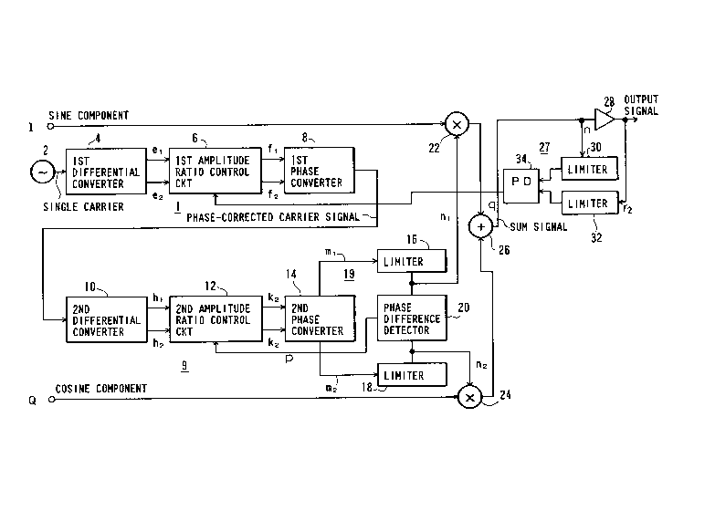
As shown in FIG. 1, a quadrature modulator, as a
first embodiment according to the present invention,
includes a first phase controller 1, serving as a phase
-- 6
2120216
difference correcting means for controlling the phase of a
single carrier outputted from the first phase controller 1
including a carrier oscillator 2, based on a phase
difference produced by an amplifier circuit 27 which
amplifies a modulated output signal. A second phase
controller 9 generates two carriers that are substantially
90 out of phase with each other, with the single carrier
whose phase has been controlled by the first phase
controller 1. The difference between 90 and the phase
difference between the two carriers is eliminated by a
carrier generator 19. Two multipliers 22, 24 multiply the
carriers, the phase difference between which has been
controlled so as to be 90 by the carrier generator 19, by
respective sine and cosine components of a baseband signal.
An in-phase adder 26 adds the product output signals from
the respective multipliers 22, 24.
The output signal from the in-phase adder 26 is
amplified by the amplifier circuit 27, which outputs the
amplified signal as a quadrature-modulated signal.
The phase controller 1 comprises a first differen-
tial converter 4 for differentially converting the output
carrier from the carrier oscillator 2 into positive- and
negative-phase carriers e1, e2 that are 180 out of phase
with each other, a first amplitude ratio control circuit 6
for controlling the amplitude ratio of the positive- and
negative-phase carriers e1, e2 outputted from the first
differential converter 4 based on the phase difference from
2120216
the amplifier circuit 27, and a first phase converter 8 for
converting positive- and negative-phase carriers f1 and f2
whose amplitude ratio has been controlled by the first
amplitude ratio control circuit 6 into the single carrier g
with its phase based on the amplitude ratio of the positive-
and negative-phase carriers f1 and f2.
As shown in FIG. 2, the first differential con-
verter 4 comprises a differential amplifier including tran-
sistors Q41 and Q42, a constant-current supply circuit 43,
and a constant-voltage supply 44. The carrier outputted
from the carrier oscillator 2 is applied to the base of the
transistor Q41, whereas the voltage from the constant-
voltage supply 44 is applied to the base of the transistor
Q42. The positive- and negative-phase carriers e1, e2 are
produced from the respective collectors of the transistors
Q41 and Q42.
As shown in FIG. 3, the first amplitude ratio con-
trol circuit 6 comprises a double-balanced differential am-
plifier including transistors Q61 - Q66 and a constant-cur-
rent supply circuit 61. The positive-phase carrier e1 is
applied to the bases of the transistors Q61 and Q64, whereas
the negative-phase carrier e2 is applied to the bases of the
transistors Q62 and Q63. To the bases of the transistors
Q65 and Q66, there is applied an output signal s from a
phase comparator 34 of the amplifier circuit 27. Output
signals produced from the collectors of the transistors Q61
and Q63 are supplied as the positive- and negative-phase
2120216
carriers f1 and f2 whose amplitude ratio has been controlled
to the first phase converter 8.
As shown in FIG. 4, the first phase converter 8
comprises a buffer amplifier 81 for being supplied with the
positive-phase carrier f1, a buffer amplifier 82 for being
supplied with the negative-phase carrier f2, and a phase
shifter 85 composed of a capacitor 83 and a resistor 84 that
are connected in series with each other. The positive-phase
carrier f1 that has passed through the buffer amplifier 81
and the negative-phase carrier f2 that has passed through
the buffer amplifier 82 are applied to the respective
opposite terminals of the phase shifter 85, and the phase-
controlled single carrier g is outputted from the junction
between the capacitor 83 and the resistor 84.
The second phase controller 9 comprises a second
differential converter 10 for differentially converting the
carrier g from the first phase converter 8 into positive-
and negative-phase carriers h1 and h2, a second amplitude
ratio control circuit 12 for controlling the amplitude ratio
of the positive- and negative-phase carriers h1 and h2
outputted from the second differential converter 10 based on
a detected phase difference signal p outputted from a phase
difference detector 20, and a second phase converter 14 for
converting positive- and negative-phase carriers k1 and k2
whose amplitude ratio has been controlled by the second
amplitude ratio control circuit 12 into two carriers m1 and
m2 the phase difference between which is based on the
2120216
amplitude ratio of the positive- and negative-phase carriers
k1 and k2.
The second differential converter 10 is identical
in structure to the first differential converter 4, and the
second amplitude ratio control circuit 12 is identical in
structure to the first amplitude ratio control circuit 6.
The carrier generator 19 comprises the second
phase controller 9, a pair of limiters 16 and 18 for
limiting the respective amplitudes of the carriers m1 and
m2 outputted from the second phase controller 9, and the
phase difference detector 20. The phase difference detector
20 detects the difference between 90 and the phase
difference between a carrier n1 whose amplitude has been
limited by the limiter 16 and a carrier n2 whose amplitude
has been limited by the limiter 18, and outputs the detected
difference as the detected phase difference signal p to the
second amplitude ratio control circuit 12. The carrier n1
is also supplied to the multiplier 22, and the carrier n2 is
also supplied to the multiplier 24.
As shown in FIG. 5, the second phase converter 14
comprises a buffer amplifier 141 for being supplied with the
positive-phase carrier k1, a buffer amplifier 142 for being
supplied with the negative-phase carrier k2, a phase shifter
145 composed of a capacitor 143 and a resistor 144 that are
connected in series with each other, and a phase shifter 148
composed of a resistor 146 and a capacitor 147 that are con-
nected in series with each other. The positive-phase
-- 10 --
2120216
-
carrier k1 that has passed through the buffer amplifier 141
and the negative-phase carrier k2 that has passed through
the buffer amplifier 142 are applied to the respective
opposite terminals of each of the phase shifters 145, 148.
The phase-controlled carrier m1 is outputted from the
junction between the capacitor 143 and the resistor 144, and
the phase-controlled carrier m2 is outputted from the
junction between the resistor 146 and the capacitor 147.
As shown in FIG. 6, the phase difference detector
20 comprises a balanced modulator circuit composed of tran-
sistors Q201 - Q206, constant-voltage supplies 207 and 208,
and a constant-current supply circuit 209, and an integrator
2010 for integrating an output signal from the balanced
modulator circuit. The amplitude-limited carrier n1 is
applied to the bases of the transistors Q201 and Q204. The
voltage from the constant-voltage supply 207 is applied to
the bases of the transistors Q202 and Q203. The amplitude-
limited carrier n2 is applied to the base of the transistor
Q205. The voltage from the constant-voltage supply 208 is
applied to the base of the transistor Q206. An output
signal from the collector of the transistor Q204 is
integrated by the integrator 2010, which outputs an
integrated signal as the detected phase difference signal p.
The balanced modulator circuit delivers an output signal x
representing the product of the carriers n1 and n2.
Depending on a shift from 90 of the phase difference
between the carriers n1 and n2, the detected phase
2120216
difference signal p is of a value reduced or increased from
the output signal at the time the phase difference between
the carriers n1 and n2 is 90.
The output signals from the respective multipliers
22, 24 are added in phase by the in-phase adder 26, which
supplies a sum output signal q, i.e., a quadrature-modulated
output signal to the amplifier circuit 27. The amplifier
circuit 27 comprises an amplifier 28 for amplifying the sum
output signal q, two limiters 30 and 32 for limiting the
amplitudes of the sum output signal q, i.e., an input signal
r1 applied to the amplifier 28, and an output signal r2 from
the amplifier 28, and a phase comparator 34 for comparing
the phase of the sum output signal q that has been limited
in amplitude by the limiter 30 and the phase of the output
signal rz that has been limited in amplitude by the limiter
32, and outputting a compared phase output signal s to the
first amplitude ratio control circuit 6.
Operation of the quadrature modulator according to
the present invention will be described below. The carrier
outputted from the carrier oscillator 2 is differentially
converted by the first differential converter 4 into the
positive- and negative-phase carriers e1, e2 which are 180
out of phase with each other that are outputted from the
respective collectors of the transistors Q41, Q42. The
amplitude ratio of the positive- and negative-phase carriers
e1, e2 is controlled by the first amplitude ratio control
circuit 6 based on the compared phase output signal s. The
- 12 -
2120216
positive- and negative-phase carriers f1 and fz whose
amplitude ratio has been controlled are converted by the
first phase converter 8 into the carrier g whose phase is
based on the amplitude ratio. Thus, the carrier g has its
phase based on the compared phase output signal s.
In the first amplitude ratio control circuit 6
shown in FIG. 3, the potentials at the bases of the transis-
tors Q65 and Q66 vary depending on the compared phase output
signal s, the balanced conditions of currents flowing
through the differential pairs of the transistors Q61 and
Q62 and the transistors Q63 and Q64 are controlled by the
amplitudes of the carriers e1 and e2, and the balanced
conditions of the amplitudes of output signals from these
differential pairs of the transistors Q61 and Q62 and the
transistors Q63 and Q64. The collectors of the transistors
Q61 and Q63 output the amplitude-controlled positive- and
negative-phase carriers f1 and f2, and supply them to the
first phase converter 8.
The positive- and negative-phase carriers f1 and
f2 outputted from the first amplitude ratio control circuit
6 are applied through the respective buffer amplifiers 81,
82 to the phase shifter 85. It is assumed that a current i
flows through the phase shifter 85, the capacitor 83 has an
electrostatic capacitance C, and the resistor 84 has a
resistance R. If the applied positive- and negative-phase
carriers f1 and f2 have the same amplitude, then the carrier
g outputted from the phase shifter 85 has a phase ~ as shown
2120216
in FIG. 7. If the applied positive- and negative-phase
carriers f1, f2 have different amplitudes, then the carrier
g outputted from the phase shifter 85 has a phase ~' as
shown in FIG. 8. Therefore, the phase ~ of the carrier g
varies based on the applied compared phase output signal s,
and hence becomes a phase ~0 which is corrected out of a
phase distortion caused by the amplifier circuit 27.
In FIGS. 7 through lO, the angular frequency of
the carriers is indicated by ~.
The carrier g is differentially converted by the
second differential converter 10 into positive- and
negative-phase carriers h1, h2 which are in phase and 180
out of phase with the carrier g. The amplitude ratio of the
positive- and negative-phase carriers h1 and h2 is
controlled by the second amplitude ratio control circuit 12
based on the detected phase difference signal p. Positive-
and negative-phase carriers k1 and k2 whose amplitude ratio
has been controlled are then converted by the second phase
converter 14 into respective carriers m1 and m2 whose phases
are based on the amplitude ratio. Therefore, the carriers
m1 and m2 have a phase difference that has been corrected
based on the detected phase difference signal p.
The second differential converter 10 operates in
the same manner as the first differential converter 4, and
the second amplitude ratio control circuit 12 operates in
the same manner as the first amplitude ratio control circuit
6.
- 14 -
2120216
The positive- and negative-phase carriers k1 and
k2 outputted from the second amplitude ratio control circuit
12 are applied through the respective buffer amplifiers 141
and 142 to the phase shifters 145 and 148. It is assumed
that a current i1 flows through the phase shifter 145, a
current i2 flows through the phase shifter 148, the
capacitors 143 and 147 have respective electrostatic
capacitances C1 and C2, and the resistors 144 and 146 have
respective resistances R1 and R2. If the applied positive-
and negative-phase carriers k1 and k2 have the same
amplitude, then the carriers m1 and m2 outputted from the
respective phase shifters 145 and 148 have a phase
difference ~1 as shown in FIG. 9. If the amplitudes of the
applied positive- and negative-phase carriers k1 and k2 are
brought out of balance, and hence the applied positive- and
negative-phase carriers k1 and k2 have different amplitudes
(the amplitude of the carrier k1 > the amplitude of the
carrier k2), then the carriers m1 and m2 have a phase
difference ~2 as shown in FIG. 10, so that the phase
difference ~ between the carriers m1 and m2 is varied based
on the detected phase difference signal p. The amplitude
ratio of the carriers k1 and k2 is thus controlled to
achieve a phase difference ~ (= 90) which eliminate the
detected phase difference signal p.
The amplitudes of the carriers m1 and m2 outputted
from the second phase converter 14 are limited respectively
by the limiters 16 and 18. Carriers n1 and n2 whose
- 15 -
2120216
amplitudes have been limited by the limiters 16 and 18 are
supplied to the phase difference detector 20 which detects
the difference between 90 and the phase difference between
the carriers n1 and n2. The phase difference detector 20
supplies a detected output signal as the detected phase
difference signal p to the second amplitude ratio control
circuit 12. Therefore, the phase difference ~ between the
carriers n1 and n2 is controlled into 90.
The carrier n1 is also supplied to the multiplier
22 which multiplies the carrier n1 by a sine component of
the baseband signal, and the carrier n2 is also supplied to
the multiplier 24 which multiplies the carrier n2 by a
cosine component of the baseband signal. Product output
signals from the multipliers 22, 24 are added by the in-
phase adder 26, whose sum output signal is amplified by the
amplifier 28. The amplified signal is outputted as a
quadrature-modulated signal.
The amplitudes of the signals inputted to and out-
putted from the amplifier 28 are limited by the limiters 30,
32, respectively. The phases of limited output signals from
the limiters 30, 32 are compared by the phase comparator 34,
which supplies a compared phase output signal to the first
amplitude ratio control circuit 6. The first amplitude
ratio control circuit 6 controls the amplitude ratio to
correct a phase distortion caused by the amplifier 28.
The first phase controller 1 composed of the first
differential converter 4, the first amplitude ratio control
- 16 -
2120216
circuit 6, and the first phase converter 8 is inserted be-
tween the carrier oscillator 2 and the second differential
converter 10. However, the first phase controller 1 may be
connected between the in-phase adder 26 and the amplifier 28
to control the phase difference between the carriers
supplied to the multipliers 22, 24 into 90 for outputting a
quadrature-modulated signal that has been corrected out of a
phase distortion caused by the amplifier 28.
As shown in FIG. 11, in a quadrature modulator as
a second embodiment according to the present invention, the
arrangement of the first phase controller 1 and the second
phase controller 9 is inverted from that of the first
embodiment described above. The first and second phase
controllers 1 and 2 comprise respectively the same
components as those in the first embodiment. Therefore, a
detailed description of the second embodiment is omitted.
Although certain preferred embodiments of the pre-
sent invention have been shown, it should be understood that
various changes and modifications may be made therein
without departing from the scope of the appended claims.