Note: Descriptions are shown in the official language in which they were submitted.
ENGLISH TRANSLATION OF ~'YENDED
_
DISCLOSURE PAGES 1 TO 12 AND
Ar5ENDED CLAIMS 1 TO 22 SUBMITTED
OCTOBER 20, 1993.
2 1 2 0 3 2 6 ~i
SUBSTITUTE SHEETS
Apparatus Assembly of an Electrotechnical Apparatus
Technical Field
The invention relates to an apparatus assembly of an
electrotechnical apparatus
(a) the housing wall of which consists of plate-
shaped elements,
(b) at least part of the plate-shaped elements being
synthetic plastic plates
(c) which are metal-coated on one side,
(d) the metal-coated surfaces being interconnected
electrically conductively.
Background Art
Housings for electrotechnical apparatus are known in
numerous forms. In the following, electrotechnical
apparatus designate apparatus which are composed of
mechanical, electromechanical and/or electronical
elements. Among other things, the housings serve for
protection of the elements arranged in the housing
against external influences. The extrenal influences
can be mechanical effects and also atmospheric
influences or similar external influences. If the
housing is made of metal, it can also protect the
elements arranged in the housing against influences of
electrical or electromagentic fields (EMV-protection,
high-voltage protection and the like). Elements can be
arranged on the inner walls of the housing or on
2 0 3 2 ~
plates or walls arranged within the housing, which
elements serve for accommodation and guiding of
printed circuit boards or boards, on which mechanical,
electrical, electromechanical or electronical elements
are arranged. In the housings printed circuit boards
or boards can be arranged, which are provided with
card plugs and are located one below the other for
connection of the individual printed circuit boards or
cards. The individual elements can be arranged on the
printed circuit boards or cards by means of the SMD-
technique. Apertures can be provided in the outer
walls of the housing, which apertures serve for
accommodation of appartus plugs and/or test plugs. The
housing walls can consist of interconnected plate-
shaped elements. Thereby, the size and shape of the
housing can easily be adapted to the respective
requirements and the manufacturing costs are
considerably reduced with small and medium piece
numbers. By the use of flexible connections in the
SMD-technique it is no longer necessary to use cable
trees for connection of individual assemblies, which
cable trees are costly in manufacturing, the layout of
which requires apertures and supports and with which
connection errors cannot always be avioded. Without
large efforts and expensive preparations, it is
possible to test individual assemblies or a plurality
of assemblies, without total assembly of the apparatus
being required. This results in reduction of the
working time required for assembling the apparatus and
of the numbers of elements, and in a reduction of the
time for checking. Nevertheless, the individual
elements and assemblies remain easily available.
From DE-OS 34 17 451 a cuboid push-in housing for
electronical apparatus is known, into which housing
insert card type modular push-in units and the like
can be inserted, the cover plate, the bottom plate,
the side plates and bars of which housing consist of
3 ~120~26~
an integral moulded synthetic plastic part, the
housing being provided with an electrically conductive
or ferromagnetic layer on the inside and/or outside.
This coating is preferrably provided on all sides.
However, with this housing it is not provided to
design the housing wall itself as printed circuit
boards.
From US-A-4 758 459 a housing is known, the outer
surfaces of which can be metal-coated, if required.
Within the housing printed circuit boards are
arranged, which can be mechanically connected to the
housing walls. The interconnection of the printed
circuit boards and the lead-out conductors thereof are
effected by a wiring arranged centrally in the
housing.
The component assembly of printed circuit boards by
means of the SMD-technique using adehesive connections
is known from Miszak Jerzy "Der Einsatz von
Klebstoffen in Mikroelektronik, Mikrotechnik und
Telekommunikation", Technische Rundschau, 20/86, p.
50-53, and the connection of a flex band to a printed
circuit board is known from DE-OS 35 00 411.
Furthermore, from DE-OS 39 28 461 an assembly support
having two metallic side walls is known, between
which, at the four edges thereof, profile bars of
metal extend, which are attached to the side walls and
carry guiding supports, which are designated for
accommodation of assemblies.
From DE-PS 32 11 758 a housing for the electrical
communication technology is known, which has a sheet
metal frame of the housing and the individual mutually
screened plug-in units of which consist of boat-shaped
sheet metal elements.
4 ~20~2~
Disclosure of Invention
It is the object of the invention to provide an
apparatus assembly of an electrotechnical apparatus,
the housing walls of which consist of plate-shaped
elements and the dimensions and weight of which are
considerably reduced as compared to the known
constructions. This reduction is highly desirable and
of great advantage in almost all applications,
particularly in the aircraft and space technology.
With the apparatus assembly, according to the
invention, these advantages are to be achieved without
affecting other important properties, particularly as
far as the protection of the apparatus against
mechanical influences such as shock, vibration,
influences of temperature, humidity and the like and
also the protection against electrical and
electromagnetic fields (EMV-protection, high-voltage
protection and the like) is conserned. Finally, is
shall be possible to assemble the apparatus assembly
without substantial expenditure of work and at low
costs.
According to the invention this object is achieved by
an apparatus assembly according to the preamble, in
which
(e) one or several of the metal-coated synthetic
plastic plates are designed as printed circuit
boards in such a manner that they are provided
with electrical and/or mechanical elements on the
side which is not metal-coated and, as the case
may be, provided with strip conductors,
CA 02120326 1998-09-22
(f) and plate-shaped elements of metal, if present,
are electrically conductively connected to the metal-
coated surface of the synthetic plastic plates.
In a further aspect, the present invention provides an
electrotechnical apparatus assembly comprising a
housing having plural walls, housing plates having
first and second opposite surfaces forming said walls,
at least portions of said housing plates being of
synthetic plastic material, each housing plate having a
continuous metal coated area on the first surface, said
metal coated areas of interconnected walls being
electrically conductive, at least one of said housing
plates being printed circuit boards, wherein components
of the printed circuit board are on the second surface,
plural metal plates being in electrical conductive
connection with the metal coated surface areas of said
housing plates.
Modifications of the invention are subject matter of
the sub-claims.
An embodiment of the invention will now be described in
greater detail with reference to the accompanying
drawings.
Brief Description of the Drawings
Fig. 1 shows a plan view of the apparatus assembly
with the top cover removed.
Fig. 2 shows a section through the apparatus
assembly taken along the line II-II in Fig.
1.
CA 02120326 1998-09-22
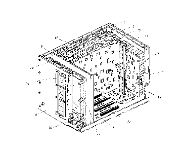
Fig. 3 is a perspective opened view of the apparatus
assembly according to the Figs. 1 and 2.
Fig. 4 shows the apparatus assembly according to
Fig. 3 after further printed circuit boards
and the front and back wall have been
removed.
Fig. 5 shows a part of a side wall with angle
brackets arranged thereon.
Fig. 6 shows the electrically conductive connection
of a side wall to an angle bracket.
Fig. 7 shows the arrangement of a card plug on a
bottom plate.
6 ~1~0~2~-~
~ig. 8 shows, in simplified perspective plan view,
the connection of a rigid printed circuit
board to strip conductors arranged on a
flexible support.
Fig. 9 shows, as detail from Fig. 8, partial sections
of a rigid printed circuit board and a
flexible part before the connection has been
established.
Preferred Embodiment of the Invention
In Figs. 1 and 2 the side walls are designated by
numerals 1 and 2, and in Fig. 2 the bottom is
designated by numeral 3. Side walls and bottom consist
of synthetic plastic material reinforced by glass
fibers or carbon fibers and are metal-coated over the
total surface or laminated with a metal layer,
particularly of copper, on their outsides. The metal
coating also extends on the intersection edges of
these plate-shaped elements 1, 2, and 3. Thereby, the
metal coatings on the outside of the plate-shaped
elements 1, 2, and 3 are conductively interconnected,
although also further conductive connections not
illustrated in the drawing can be present. The top
cover designated by numeral 4 in Fig. 2 consist of
aluminum, and also the front wall 5 and back wall 6
visible in Fig. 1. The walls 5 and 6 are conductively
connected to the metal-coated surfaces of the side
walls 1 and 2 and of the bottom 3. Angle brackets 7
serve for mechanical connection, which angle brackets
can consist of extruded aluminum.
As can be seen from Figs. 1 and 3, partitions 8 and 9
extend between the side walls 1 and 2 parallelly to
the front wall 5 and to the back wall 6, respectively,
and spaced therefrom. These partitions 8 and 9 consist
of aluminum. They extend vertically from the bottom 3
f ~ ~! Q 3 2 ~
to the top cover 4. A printed circuit board 10 is
located in the space between the back wall 6 and the
partition 9, and in the same way a printed circuit
board 11 is located between the front wall 5 and the
partition 8. The printed circuit boards 10 and 11 are
mechanically connected to the front wall 5 and the
back wall 6, respectively, through spacers 12 and 13,
respectively. Particularly when apertures for
apparatus plugs 14 and test plugs, respectively, are
provided in the front wall and/or the back wall 6, the
spaces, in which the printed circuit boards 10 and 11
are located, are not as completely protected against
the influence of magnetical or electromagnetic fields
as the space between the partitions 8 and 9. Elements
can be arranged on the printed circuit boards 10 and
11, which elements, in this respect, do not require
the best protection as possible as, for example,
filter assemblies, high-voltage protectors and the
like. The printed circuit boards 10 and 11 can also be
provided with the apparatus plugs 14 and the test
plugs, respectively. Apart from that, the component
assembly of the printed circuit boards 10 and 11 can
also be effected on both sides. The electrical
connection of the printed circuit boards 10 and 11 to
the bottom plate 3 is effected by flexible connecting
strips 16. These are strips and tapes, respectively,
of a flexible non-conductive foil material, on which a
plurality of strip conductors are provided. These
flexible connecting strips 16 and the connection of
their strip conductors to the strip conductors of
those printed circuit boards, on which they are
arranged, are described below in further detail.
Guiding devices 17 for printed circuit boards 18 are
provided on the inner sides of the partitions 8 and 9.
The guiding devices 17 and the associated locking
deices 19 are only schematicly illustrated in the
drawings. The printed circuit boards 18 are equipped
8 ~ ~ ~ Q 3 2 B
with components on both sides, at least partly. There
is a large freedom in the choice of the component
assembly technique, the connection can be effected by
means of the wire ends of the components or the
components can be mounted on the printed circuit
boards by means of the SMD-technique; the printed
circuit boards can be provided with bores and/or be
through-connected or, in particular when the SMD-
technique is used, can be provided without bores or
through-connections.
The connection of the printed circuit boards 18 to the
bottom plate 3 is effected through card plugs 20, 21.
The parts 20 thereof are attached to the printed
circuit boards 18, while the parts 21 thereof are
arranged on the bottom 3. As can be seen from Fig. 7,
the arrangement of the plug parts 21 on the bottom 3
is effected in such a manner that an electrical
connection of the electrically conductive elements
provided in the plug portion 21 indeed exists with the
strip conductors arranged on the upper side of the
bottom plate 3, but not with the metal coating 22
located on the underside of the bottom plate 3.
Fig. 4 shows, in the same illustration as Fig. 3, a
similar apparatus assembly, in which, however, the
printed circuit boards 18 and the partitions 8 and 9
are omitted. The angle bracket serving to attach the
partitions 8 is designated by numeral 23. The outside
of the side wall 1 not visible in Figs. 3 and 4 is
metal-coated over all of the surface. As can be seen
in particular from Fig. 4, the side of the side wall 1
facing the interior of the apparatus is designed as
printed circuit board and, to this end, provided with
strip conductors and equipped with elements 24 in SMD-
technique. As can be seen from Fig. 5, the side wall 2
is designed correspondingly. Whith this design of the
side walls 1 and 2, their sides of the printed circuit
3 ~
board directed to the interior of the apparatus and
their continuous metal-coated outside surfaces are
electrically independent of each other. The electrical
connection of the sides of the printed circuit boards
of the side walls 1 and 2 to the bottom plate 5 is
effected through flexible connecting strips 16.
By the above described design of the side walls 1 and
2 as printed circuit boards on one side, a
considerable reduction of the volume and the weight of
the apparatus assembly is effected. The reduction of
weight corresponds to the weight of two printed
circuit boards (equipped on one side) or one printed
circuit board (equipped on both sides) and the
required space is reduced correspondingly. A further
reduction of weight is achieved in that aluminum is
not used for the side walls 1 and 2 but a specifically
substantially lighter synthetic plastic material
reinforced by glass fibers or carbon fibers, the
mechanical properties of which are at least equal to
those of aluminum. The same also holds true for the
bottom 3 consisting of metal-coated synthetic plastic
material.
Care is taken that the metal-coated or metal laminated
outer surfaces of the side walls 1 and 2 and the
bottom 3 are in reliable electrically conductive
connection with the structure elements of the
apparatus assembly consisting of metal, as, for
example, the top cover 4, the front wall 5, the back
wall 6, the partitions 8 and 9 and the angle brackets
7 and 23.
An example of a direct electrically conductive
connection is illustrated by means of Fig. 6. Therein,
a section of one of the angle brackets 7 visible in
Fig. 4 is designated by numeral 27. A grounding spring
strap 28 is arranged, electriclly conductively
CA 02120326 1998-09-22
connected, on the leg which the side wall 1 (or 2)is
to engage. The side wall 1 is metal-coated over all of
its surface on its top surface as viewed in the plane
of the drawing. The metal coating also extends over
the intersection edges 29 and 30 and, not visible in
the drawing, over the edge area of the side of the
side wall 1 which is not metal-coated over all of its
surface. All of these metal coatings are conductively
interconnected. In order to establich the conductive
connection between the angle brackets 27 and the side
part 1, the side part 1 is pressed with its metal-
coated edge area, not visible in the drawing, against
the grounded spring strap 28.
A flexible connecting strip 16 with the strip
conductors 31 located thereon and their electrically
conductive connection, not shown in the drawing, with
strip conductors on the bottom plate 3 are shown in
the Figs. 8 and 9. Instead of the bottom plate 3 the
connection can also be with one of the side walls 1, 2
or of another printed circuit board as, for example,
10 or 11. A connection generally designated by numeral
32 is illustrated in detail by means of Fig.9. The
rigid bottom plate 3 consists of non-conductive
synthetic plastic material reinforced by glass fibers
or carbon fibers. It can also consist of a non-
conductive ceramic material. The flexible connecting
strip 16, which also is called "flex", can be a foil
consisting of a thermostable polyimide, for example
Kapton of Du Pont. In the graphical illustration of
Fig. 8, the strip conductors 31 are located on the
underside of the flexible strip 16. The strip
conductors located on the rigid printed circuit board
3 are not illustrated in Fig.8. The individual
connections generally designated by numeral 32 are
further described in the following by means of Fig.9.
*Trade Mark
CA 02120326 1998-09-22
In the lower part of Fig. 9 a strip conductor 33 is
located on the rigid printed circuit board 3
illustrated sectionally, which strip conductor 33
communicates with a solder plate 34 electrically
connected thereto. The strip conductor 33 and the
solder plate 34 are manufactured in known manner, for
example by etching, and can have different thicknesses
if desired. At least the solder surface 34 is tinned
or coated by a solder paste known from the SMD-
technique.
A cover foil 35 preventing the solder flux is located
on the upper surface of the rigid printed circuit
board 3. The cover foil 35 is shaped such that the
soldering surface 34 is freely accessible from the top
while it can cover the strip conductor 33. Instead of
the cover foil also a correpondingly formed coating of
a solder stop lacquer can be used. The surface of the
soldering surface 34 is located slightly deeper as the
surface of the cover foil 35 preventing the solder
flux.
A strip conductor 31 consisting of copper is located
in the upper part of Fig.9 below the foil 16 serving
as flexible printed circuit board, which strip
conductor 31 can be narrower than illustrated in the
drawing. A soldering surface 36 is located below the
strip conductor 31 and is connected thereto. The
soldering surface 36 has a hollow cylindrical shape
and has larger hight and thickness than the strip
conductor 31. Its lower annular surface facing the
soldering surface 34 is tinned or coated by a solder
paste containing tin. The outer diameter of the
annular surface is smaller than the side length of the
square soldering surface 34 or the section formed in
the cover foil 35, respectively. A cover foil 37
preventing the solder flux is located on the underside
of the strip conductor 31, which cover foil 37,
CA 02120326 1998-09-22
however, does not cover the annular soldering surface
36 facing the soldering surface 34. Instead of the
cover foil preventing the solder flux also a layer of
solder stop lacquer can be used.
In the area of the soldering surface 36 and through
it, a check bore 38 extends through the flexible foil
16 and the strip conductor 31. The underside of the
cover foil 37 preventing the solder flux is coated by
a heat curable plastic adhesive.
In order to join the connections, the printed circuit
boards 3 and 16 are fittedly pressed one upon the
other and heated on both sides, at least, however, on
the outside of the printed circuit board 16. The
heating can, for example, be effected by means of a
correspondingly large plane surface of an instrument
similar to a soldering bit. Thereby, the tin located
on the soldering surfaces 34 and 36 is melted and
connects the soldering surfaces with each other. At
the same time the adhesive layer 39 is hardened and
establishes a reliable mechanical connection between
the printed circuit boards 3 and 16. The quality of
the solder connections can be checked optically
through the check bores 38.
By the connection described above, a metal coating or
metallic lamination located on the side of the printed
circuit board 3 opposite the connections is completely
unspoiled and unaffected.