Note: Descriptions are shown in the official language in which they were submitted.
2121~10
,
INSUL~TED CONL~U~:1Ok PAIRS AND ME1~IOD
AND APP~RATUS OF M~KING SAME
Field of the Invention
The present invention relates to conductors and, more
particularly, to insulated conductor pairs.
Backqround and SummarY of the Invention
The use of conductors arranged in palrs is well known
from the use of such conductor pairs in telephone circuitry
and other high-frequency applications. Such conduc~or pairs,
and conductors generally, are used in situations where, for
example, it is necessary to extend large quantities of
conductors between two points. To avoid checking each
conductor of a large number of conductors for conductivity at
each end of a plurality of conductors, various means ~or
identifying the individual conductors of the plurality of
conductors have been devised. Among the more popular means of
identifying individual conductors is through the use of a
color code system, whereby individual conductors are coated
with differently colored insulating material for purposes of
identification. other techniques for identifying individual
conductors include the printing of markings such as stripes or
words on the insulating material.
The great need for conductor pairs in applications such -
as those noted above has been a motivating factor in the
development of a highly competitive industry in manufacturing
such conductor pairs, and has led to a variety of techniques
for manufacturing such conductor pairs. According to one
technique, individual conductors are coated with an insulating
material and subsequently bonded together by, for example, an
~c:\specs\506xO07\dv~ 1
2121110
adhesive (herein referred to as a "bonded pair"). According
to another technique, lndividual, substantially parallel
conductors are guided through an extruder apparatus in which
they are both covered with insulating material in a single
coating operation so that they are extruded t:ogether in an
attached form or are forced together so that they attach to
one another shortly after being extruded (herein referred to
as an "attached pair"). The individual conductors of an
bonded or attached pair are preferably separable by breaking a
web or attachment point between them so that their ends can be
connected to desired connectors.
It is particularly useful to be able to identify
conductors as part of a conductor pair. Earlier methods of
identifying conductors as part of a conductor pair included
simply twisting a pair of wires together. More advantageous
methods of identifying conductors as part of a conductor pair
include the above-mentioned techniques for forming bonded
pairs or attached pairs to avoid the likelihood of separation
of conductor pairs that are not physically joined. Further,
it has been found to be desirable to provide color code
markings on individual ones of the conductor pairs to
facilitate identification of the conductor pairs.
Industry standards such as those of the National
Electrical Code Tm and the Insulated Cable Engineers
Association, Inc., (ICEA) have standardized color code schemes
and established guidelines for identifying conductor pairs.
For example, ICEA has promulgated Standards for Communications
Wire and Cable for Wiring of Premises setting out standards
~c:\specs\506xO07\dv~ 2
~, ~ , ~, ' !,,: ' '; ! ' ' ,., ' . .
2121110
for insulating material color combination9 for so-called "tip"
and "ring" conductors of a pair. In Section 4.4 it is stated
that, "positive identification of the associated 'tip' and
Iring' conductors of a pair shall be accomplished by marking
or striping each insulated conductor of a pair with the color
of its mate". The ICEA's Standards further note that, in
cables with five or less pairs, the marking of the ring
conductor may be omitted. It is desirable to comply with this
standard by forming a first insulated conductor that is
primarily a first color and a second insulated conductor that
is primarily a second color, and providing identification on
one or both of the conductors, in the form of a marking or
stripe of the color of the mate, so that the there is less of
the colored identification on the particular conductor than
there is of the primary color of the particular conductor.
Various difficulties are presented in marking or striping
of tip and ring conductors in conductor pairs so that they
meet industry standards. For example, conductor pairs formed
as attached pairs are typically insulated with a single
i~sulating material 50 that it is necessary to mark at least
one conductor of the pair so that it has a mark or stripe of
the color of its mate. While it is possible to provide ink
markings on each conductor of the pair, beside being subject
to smearing of the ink, as seem in FIG. lA, ink markings in
the form of stripes 21 are typically only applied over less
than half of the conductors 23, 25 so that each conductor is
more properly described as being the same color with a stripe
of a different color. Ink markings in the form of bands 27
~c: \~ipec~\506xO07\dv> 3
.
.:; , :
.. ~ :. . . ::
,
2~ 21~10
.
are shown in FIG. lB are also typically applied over less than
half of the conductors 23, 25 so that each conductor is
properly described as being the same color with a stripe of a
different color. Further, band marking of conductors is
preferably performed on a single insulated conductor prior to
forming a bonded pair or an attached pair, rather than in
applications involving attached pairs that are extruded as
attached pairs.
Another technique for applying color coding stripes is
the coextrusion technique described ln U.S. Patent Nos.
2,521,123, 3,288,895, and 4,248,824. In U.S. Patent No.
3,2~8,895, in which a pair of conductors is produced, a main
extruder feeds the main insulating material into a main
extruder die and stripes of colored material are fed into the
main extruder die from auxiliary extruders to form stripes on
a pair formed of another color. However, the thickness of the
colored material materially alters the unit capacitance of the
conductor and maintaining capacitance balance in the pair
requires optimization of the depth of the stripes. Further,
.
as shown herein at FIG. lC, the pair of insulated conductors
23, 25 does not produce two conductors that are primarily
different colors but, rather, includes two conductors that are
both primarily one color, with a stripe 29 along the length of
at least one of the conductors.
U.S. Patent No. 3,720,747 to Anderson et al. describes
yet another technique for color coding multiple conductors in
which insulating material of desired colors is arranged in a ~ -
preform, and the preform is placed in an extruder. While the ~-
~c:\spec~\506xO07\dv~ 4
' . : ~ ..: .",::.. .':: :-,,,.:- :: ::: :., : :, :
: ~ : ' ' ,: ~:
21211~0
technique described therein is adapted to produce pairs of
conductors having primarily different colors, the technique is
complicated in that it includes a number of steps, such as
arranging the insulating material in the preform prior to
coating of the conductor with the insulating material.
In addition to the desirability of color coding conductor
pairs, it is desirable to minimize crosstalk in conductor
cables. In our co-pending U.S. application, it is noted that
it is known that twisting conductor pairs can be performed to
minimize electrical coupling between paired conductors. In
that application, the inventors recognize the benefits of
controlling center-to-center distances ln a twisted conductor
pair ~or purposes of stabilizing capacitance within a cable.
Further, the inventors recognize the benefits of controlling
center-to-center conductor spacing on all cables used in a
particular design so that impedances in the design are
matched, thereby minimizing problems with signal 105s and
tracking error (jitter). The inventors propose controlling
center-to-center spacing in twisted pair cables so that a
twisted pair cable has a center-to-center distance measured
between the centers of adjacent conductors that is +/- 0.03
times the statistical average of that distance as measured in
at least twenty measurements of each 1000 ft. of cable with
each measurement taken at least twenty feet apart.
~lternatively, or in combination, the inventors propose
providing conductors and corresponding dielectric layers
twisted along the length of a cable having, over any 1000 ft.
length of the cable, an average impedance of approximately 90
cc: \Bpec9\so6xoo7\dv~ 5
, - . ....
. . :
..
..
. : . - : . :
.. ~ ,: . . ~ , .
.. , . . : ~ :: .. .
:: , : :
,
, :. :
. , :
2121110
to 110 ohms when measured at high frequencie9 of approximately
10 MHz to approximately 200 MHz with a tolerance of +/- 5~
from an average measured from a randomly selected 1000 feet of
twisted cable. It is desirable to provide a conductor pair
combining the advantages of controlled center-to-center
distances between conductors and/or controlled impedance
characteristics proposed by Kenny and Siekierka with the
simplicity of use available in color coded conductor pairs.
Obiects and Summary.
It is an ob~ect of the present invention to provide a
conductor palr that complies with applicable industry standard
for color coding conductor pairs.
It is further an object of the present invention to -
provide a conductor pair that complies with applicable
industry standards for color coding conductor pairs and in -
which center-to-center distances between conductors in a
conductor pair are maintained within a predetermined range.
It is further an object of the present invention to
provide a conductor pair that complies with applicable -
industry standards for color coding conductor pairs and in
which impedance characteristics of the conductor palr ls
maintained within a predetermined range.
In accordance with one aspect of the present invention, a -~
conductor pair is provided including a first insulated
conductor that is primarily coated with a first insulating
material and a second insulated conductor that is primarily
coated with a second insulating material. Identification is
<c: \specs\506xO07\dv, 6
. , .
- : ~:
2l2lllo
provided on one or both of the conductors, in the form of a
marking or stripe of the color of the mate, 90 that the there
is less of the colored identification on the particular
insulated conductor than there is of the primary color of the
particular insulated conductor.
In accordance with another aspect of the invention, a
method for making an insulated conductor pair is described.
In accordance with the method, a first insulating material is
applied around a first conductor such that the first
insulating material forms more than half OLC an exterior
surface of a first insulated conductor. A second insulating
material is applied around a second conductor such that the
second insulating material forms more than hal~ of an exterior
surface of a second insulated conductor. A center--to-center
distance between the first and second conductors is maintained '
within a predetermined range.
In accordance with yet another aspect of the present
invention, in an apparatus for making an insulated conductor
pair a first insulating material and a second insulating
material are combined in an extruder apparatus. A first and a
second parallel conductor are guided by a guiding assembly
through the extruder apparatus so that the first and second
insulating materials surround at least portions of the first
and second conductors, respectively. Exterior surfaces are
formed on the first and second conductors as they are drawn
through a forming die such that the first and second
conductors having exterior surfaces form a pair of insulated
conductors. The first insulating material is formed around at
.:c: \!ipecq\506xO07\dv, 7
2121110
least half of the first conductor and the 9econd insulating
material is formed around at least half of the second
conductor.
3escri~tion of the Drawinqs
The present invention can be further understood with :
reference to the following description in conjunction with the :
appended drawings, wherein like elements are provided with the ~ ;~
same reference numerals.
FIGS. lA-lC are perspective, partially cross-sectional
views of conductor pairs including two insulated conductors :
formed primarily of the same color ln9ulation and including a . : .
longitudinal ink stripe applied to one of the conductors, a
series of circumferential bands of ink applied to one of the
conductors, and a coextruded stripe applied to one of the
conductors, respectively;
FIG. 2 is a schematic, partially cross-sectional view of - :~
an apparatus for forming a conductor pair according to an
embodiment of the present invention; : :~
FIG. 3 is a perspective, partially cross-sectional view
of a conductor pair according to a first embodiment of the
present invention; ~: :
FIG. 4 is a perspective, partially cross-sectional view
of a conductor pair according to a second embodiment of the :
present invention;
FIG. 5 is a perspective, partially cross-sectional view
of a conductor pair according to a third embodiment of the
present invention;
cc: \9p~c9\506x007\dv~ 8
21211~V
FIG. 6 is a perspective, partially cross-sectional
view of a conductor pair according to a fourth embo~;m~nt
of the present invention;
FIG. 7 is a perspective, partially cros,~-sectional view
of a conductor pair according to a fifth embodiment of the
present invention;
FIG. 8 is a perspective, partially cross-sectional view
of a conductor pair according to a sixth embodiment of the
present invention; and
FIG. 9 is a front view of an extruder apparatus arranged
for manufacturing the conductor pair shown in FIG. 8.
Detailed Description
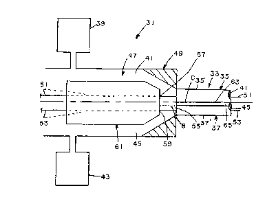
With reference to FIG. 2, an apparatus 31 for forming an
insulated conductor pair 33 including an insulated conductor
35 and a insulated conductor 37 is shown. The apparatus 31
includes a primary extruder 39 for extruding a first
insulating material 41 and a secondary extruder 43 for
extruding a second insulating material 45. The first and
second insulating materials 41, 45 may each be the same one of
any suitable material normally used in the insulation of
cables, such as polyvinylchloride, polyethylene,
polypropylene, or fluoro-copolymers (such as Teflon, which is
a registered trademark of DuPont), crosslinked polyethylene,
rubber, etc. In accordance with the preferred embodiment, the
first and second insulating materials are different colors and
are selected from the standard color combinations set forth in
the ICEA Standards at, e.g., Table 4-3.
<c: \specs\506xO07\dv, 9
.. . .. .
2121110
The primary extruder 39 and the secondary extruder 43
deliver the first and second insulating materials 41, 45,
respectively, to a chamber 47 in a die 49. The first and
second insulating materials 41, 45 are combi~ed in a ~-
controlled fashion so that they form a single insulating
material. However, the combination of the first and second
insulating materials 41, 45 is controlled so that there is
substantially no turbulence or intermingling of the first and
second insulating materials, and a well defined boundary s
between the first and second insulating materials is -
maintained.
A first conductor 51 and a second conductor 53 are guided
through the chamber 47 of the die 49, through the combined
first and second insulating material9 41, 45, and through an
opening 55 in the die in a known fashion. Preferably, the
first and second conductors S1, 53 are guided by means such as
side by .side openings 57, 59, respectively, in a guide tip 61.
The first and second conductors 51, 53 are preferably guided
so that the center-to-center distance from the first conductor
to the second conductor is ~/- 0.03 times the statistical
average of that distance in at least twenty measurements of
each 1000 ft. of cable with each measurement taken at least
twenty feet apart. The first and second conductors 51, 53 may
be constructed of any suitable material, in solid or stranded
form, including copper, metal coated substrate, silver,
aluminum, steel, alloys, or a combination thereof.
As the first and second conductors 51, 53 are guided
through the chamber 47 in the die 49, they are coated with the
~c: \specs\506xO07\dv~ 10
2121110
first and second insulating materials 41, 45. As the first
and second conductors 51, 53 are drawn through the opening 55
in the die 49 and first and second insulating materials 41, 45
on the first and second conductors ls extruded through the
opening with the first and second conductors, the first and
second insulated conductors 35, 37 having exterior surfaces
35', 37' are formed, the first and second insulated conductors
35, 37 forming the insulated conductor pair 33. As is known,
depending upon whether the insulated conductors 35, 37 are
extruded as an attached pair or are joined to one another
subsequent to exiting the die 49, such as by being forced
together or bonded together by an adhesive, the opening 55 is
a single opening of a desired, preferably figure 11811 shape,
or, preferably, two separate openings of desixed shapes,
preferably circular, respectively. The exterior surfaces 35',
37' of the first and second insulated conductors 35, 37 are
preferably substantially circular, as a result of the
peripheral shape of the opening 55 being substantially
circular or in the form of a figure 11811, and meet at a web
or attachment point 63 formed by one or both of the first and
second insulating materials 41, 45. The web or attachment
point 63 is preferably thin and weaker than the adjacent first
and second insulated conductors and thereby facilitates
separation of the first and second insulated conductors by
being easily broken. The force necessary to separate the
first and second insulated conductors 35, 37 by breaking the
web or attachment point between them is usually between 0.1
and 5 lbs force and preferably between 0.25 and 2.5 lbs force.
~c:\specs\506xoo7\dv~ 11
2l2lIf g
By controlling the rate at which the primary and
secondary extruders 39, 43 deliver first and second insulating
materials to the chamber 47 of the die 49 and controlling the
combination of the first and second insulating materials in
the chamber, it is possible to form various embodiments of the
insulated conductor pair of the present invention. For
example, when the primary extruder 39 extrudes first
insulating material 41 at a faster rate than the secondary ~'
extruder 43 extrudes second insulating material 45, the first
insulating material flows over a centerline C of the chamber
and the first and second conductors 51, 53. The insulated
conductor pair 33 that is formed has a first insulated
conductor 35 formed of the first conductor 51 having an
exterior surface 35' formed entirely of first insulating
material 41, a second insulated conductor 37 having an
exterior surface 37' formed of both first insulating material
and second insulating material 45, and a web or attachment
point 63 formed of the first insulating material. Following
extrusion of the insulated conductor pair 33 through the
opening 55, the insulated conductor pair is ordinarily
quenched, such as by immersion in a liquid such as water.
other known operations subsequent to extrusion of the
conductors include providing printed band markings on
individual conductors, usually prior to immersion in a
quenching liquid, providing printed stripes on conductors, and
providing conductor pairs with a desired twist. The insulated
conductor pair 33 preferably possesses the characteristics,
including low crosstalk and average impedance of approximately
~c: \spec3\sO6xoo7\dv:. 12
21 21110
90 to 110 ohms when measured at high frequencies of
approximately 10 MHz to approximately 200 MHz with a tolerance
of +/- 5~ from an average measured from a randomly selected
1000 feet of twisted cable, of the twisted parallel cable
described in our copending U.S. application.
By setting up the primary and secondary extruders 39, 43
to deliver first insulating material 41 and second insulating
material 45 in appropriate quantities, it is possible, through
use of the apparatus 31, to form an insulated conductor pair
33 having a first insulated conductor 35 having an exterior
surface 35' formed entirely of first insulating material ~1
and a second insulated conductor 37 having an exterior surface
37' formed primarily of second insulating material 45 and
secondarily of first insulating material. By coloring the
first and second insulating materials 41, 45 appropriately in
accordance with industry standards, the insulated conductor
pair 33 complies with those standards in that a longitudinal
stripe 65 having the coior of the exterior surface 35' of the
first insulated conductor 35 is formed on the exterior surface
37' of the second insulated conductor 37. The stripe 65 thus
formed is resistant to smearing, unlike printed stripes or
bands, and does not result in disadvantageous electrical
characteristics of the insulated conductor pair 33 in that the
stripe is formed of th~ same material as the remainder of the
insulation on the second conductor 53.
Further, insulated conductor pairs having desired
characteristics may be formed according to any desired method
whereby the first insulating material 41 is applied around the
cc: \specs\506xO07\dv~ 13
21~1110
first conductor 51 such that the first insulating material
preferably forms more than half of the exterior surface 35' of
the first insulated conductor 35. The second insulating
material 45 is applied around the second conductor 53 such
that the second insulating material preferab:Ly forms more than
half of the exterior surface 37' of the second insulated
conductor 37. The first and second insulated conductors 35,
37 are extruded through the opening 55 of a die 49 as the
insulated pair 3 3 .
At least one of the first and second insulated conductors ~ ~
35, 37 are preferably identified as corresponding to the -
conductor pair 33 including the first and second insulated
conductors. While the identification of the first and second
insulated conductors 35, 37 may be in a form such as a printed
marking, described further below, the identification of the
first and second insulated conductors is preferably performed
as a result of the ~flow over~ of at least one of the first
and second insulating materials 41, 45 to form a portion of :
the exterior 35', 37' of the first and second insulated
conductors 35, 37. ~ :
If desired, such as for purposes of identification of one
or both of the first and second insulated conductors 35, 37 or
for purposes of forming a desired thickness insulation layer
on the conductors 51, 53, the first and second insulating
materials 41, 45 is applied over an already-formed insulating
layer 67, as seen in FIG. 6, and discussed further below. The :
insulating layer 67 is formed of one of the first or second
insulating materials 41, 45, or of any desired insulating
~c:\speca\506xoo7\dv, 14
:
212~ 110
material. The insulating layer 67 is applied, as desired,
either in an entirely separate coating operation or with a
coextrusion arrangement of the type that is well known.
FIG. 3 shows a first embodiment of an insulated conductor
pair 33a. The insulated conductor palr 33a include5 a first
insulated conductor 35a and a second insulated conductor 37a.
The exterior surface 37a' of the second insulated conductor
37a is at least partially formed by first insulation material
41. The first insulation material 41 preferably forms a
longitudinal stripe along the length of the second insulated
conductor 37a for purposes of identification of that insulated
conductor as one of the pair 33a.
FIG. 4 shows a second embodiment of an insulated
conductor pair 33b. The insulated conductor pair 33b includes
a first insulated conductor 35b and a second insulated
conductor 37b. The exterior surface 37b' of the second
insulated conductor 37b is at least partially formed by first
insulating material 41. The first insulating material 41 - -
contacts the second conductor 53b. The first insulation
material 41 preferably forms a longitudinal stripe along the
length of the second insulated conductor 37b for purposes of
identification of that insulated conductor as one of the pair
33b.
FIG. 5 shows a third embodiment of an insulated conductor
pair 33c. The insulated conductor pair 33c includes a first
insulated conductor 35c and a second insulated conductor 37c.
The exterior surface 37c~ of the second insulated conductor
37c is at least partially formed by first insulating material
~c:\9pecg\506xoo7\~V~ 15
~ '
.- , , -. . .
2121110
41. The first insulating material 41 surrounds the second
conductor 53c. The first insulation material 41 preferably
forms a longitudinal stripe along the length of the second
insulated conductor 37c for purposes of identification of that
insulated conductor as one of the pair 33c.
The insulated conductor pairs 33a, 33b, :33c shown in
FIGS. 3, 4, and 5, respectively, are all preferably formed by ~ -
the previously described flow over method and apparatus
whereby the amount of first insulating material 41 delivered
to the chamber 47 of the die is larger than the amount of
second insulating material 45 delivered to the chamber so that
the controlled combination of the two insulating materials
results in desir0d amounts of first insulating material
forming the insulation around the second conductor 53.
Similarly, the web or attachment point 63 is formed by the
first insulating material 41.
FIG. 6 shows a fourth embodiment of an insulated
conductor pair 33d, such as was briefly discussed above. The
insulated conductor pair 33d includes a first insulated
conductor 35d and a second insulated conductor 37d. The first
conductor 51d is at least partially in contact with second ~ ;~
insulating material 45, or some other insulating material.
The second insulating material 45 preferably surrounds the
first conductor 51d and is applied by means of a known
coextrusion process. The second insulating material 45
preferably aids in identifying the first insulated conductor ~ ;
35d as one of the pair 33d. The second insulating material 41
may also aid in increasing the overall thickness of the first
cc:\9pec9\506xOO7\dv~ 16
': , ... . ..
' 1 . : ,,
2121110
insulated conductor. The exterior sur~ace 37d' of the second
insulated conductor 37d is preferably provided with
identifying markings such as a narrow stripe or repeating band
69. The band 69 is preferably of the same color as the first
insulating material 41. Further, the band 69 is preferably
printed on, e.g., the e~terior surface 37d' of the second
insulated conductor 37d in ink, prior to joining of the
insulated conductors 35d and 37d by bonding or otherwise
attaching them.
FIG. 7 shows a fifth embodiment of an insulated conductor
pair 33e. The insulated conductor pair 33e includes a first
insulated conductor 35e and a second insulated conductor 37e.
The exterior surface 35e' and 37e' of the first and second
insulated conductors 35e and 37e are formed entirely by first
and second insulating materials 41 and 45, respectively. As
with the insulated conductor pair 33d, at least one of the
exterior surfaces 35e' or 37e' of the first or second
insulated conductors 35e or 37e is preferably provided with -~
identifying markings such as a narrow stripe or repeating band
69. The band 69 is preferably of the same color as the
insulating material of the insulated conductor that does not
have the narrow stripe or repeating band printed thereon.
Further, the band 69 is preferably printed in ink. The web or
attachment point 63 is preferably formed by one or both of the
first and second insulating materials 41, 45.
The insulated conductor pairs 33d and 33e shown in FIGS.
6 and 7, respectively, are all shown as having no portions of
the exterior surfaces of their respec~ive first and second
~c: \spec9\506xoo7\dv:. 17
2121110
insulated conductors formed by second or fir9t insulating
material, respectively. It is understood that, if desired, as
with the insulated conductor pairs 33a, 33b, and 33c, a
portion of the exterior surfaces of one or both of the
insulated conductors of the insulated conductor pairs 33d and
33e may be formed by insulating material of the other
insulated conductor. Like the insulated conductor pairs 33a,
33b, and 33c, the insulated conductor pairs 33d and 33e are
preferably formed by the flow over method and apparatus
described above. :-
FIG. 8 shows a sixth embodiment of an insulated conductor
pair 33f. In this embodiment, the exterior surface 35f' of
the first lns~lated conductor 35~ is primarily formed by first
insulating material 41 with a smaller portion of the e~terior
surface being formed by second insulating material 45.
Likewise, the exterior surface 37f' of the second insulated
conductor 37f is primarily formed by second insulating
material 45 with a smaller portion of the exterior surface
being formed by first insulating material 41. Like the
insulated conductor pairs 33a-33e, the insulated conductor
pair 33f is preferably formed by the flow over method and ~ ~ :
apparatus 31 described above. Formation of the desired ~ :
combinations of insulating material 41, 45 on the exterior :
surfaces 35f~ and 37f' of the first and second insulated
conductors 35 and 37 is preferably accomplished by rotating
the first and second conductors 51f and 53f through a desired
angle 9 around a point at the centerline C of the apparatus
and the point of contact at the boundary B between the first
~c:\specs\506xO07\dv~ 18
:, ,
~ : ....
, h . ' . i'. ~ ~
'.~:, ' ' ' ' ' ,~, " ' ' ' ', ' , ' ' . :
' ' ' " . ' . ' I
2~2~110
and second insulating materials as shown in FIG. 9. The
opening 55, shown as a figure 11811, is also rotated through
the desired angle 9.
While this invention has been illustrated and described
in accordance with a preferred embodiment, it is recognized
that variations and changes may be made therein without
departing from the invention as set forth in the claims.
!
~c: \spec3\506xOO7\dv~ 1 9
" ':': ' ,' '~ :