Note: Descriptions are shown in the official language in which they were submitted.
t
WO 93/08464PCI/USg2/08940
2~2:~797
. ~ .
"
', ?~
..,
~ ,
;';.
'~ METHOD AND DEVICE FOR BIOCHEMICAL SENSING
; i RELATIONSH~P TO EARLIER FILED APPLICATION
. : This application claims priority from United States patent application serial number
i~ 07/781,479, filed on October 21, 1991.
FIELD QF THE INVENTION
This invention relates to sensin~ and measurin~, chemicals in general, and more particularly tO
me2hods and apparatus for sensinG and mcasurin~ chemicals, biochemicals, molecules and sub-
molecular components includin~ ions, usin~ semiconductor sensors.
~ACKGROUND OF THE INVENTlON
10 Semiconductor sensors for deSectin~ biochemical reactions are known in the art, as exemplified
by U.S. patent no. 4,180,771 to Guckel (1979). Fi~ure 1 depicts a typical such prior art
:~ sensor 2 used to rneasure the attachment to a solid substrate surface 4 of a desired chemisal
~: compound 6 in a solution 8.
:.
. Sensor 2 typically is fabricated like a metal oxide silicon I~MOS~) field effect transistor, where-
in re~ion 10 functions like a channel between souree ~nd drain regions 12, 14, and re~ion 16
functions like a ~ste, but without metalization. Usin~ receptor-type mechanisms 18, re~ion
4 is made sensitive to ~and encoura~es adhesion or attraction with~ a desired tar~et substance
6. Alternatively, receptor-like mechanisms 18 may be attached to the device ~ate 16.
Althou~h re~ion 4 should be relatively insensi~ive and non-reactive to other chemicals, such
as 20, but in practice re~ion 4 can respond non-specifically and sttach with other than desired
tar~et substance 6. For example, solution 8 may also include char~ed particles 22 ot varyin~
size, includin~ positive and ne~ative ions. In biochemical sensin~ applications, a suitable
biochemical environment tor the receptor 18 and bio-tar~et 6 dictates that test solution 8 have
a relatively lar~e ionic concentration. Unfortunately, rslatively lar~e ion concentration for the
test solution 8 can adversely affect biochemical measurement due to ionic shieldin~.
.
WO g3/08464 2 1 2 1 7 9 ~ PCI`~US92/08940
--2--
Prior art measurements use a reference electrode to obtain stable and reproducible measure-
;, ments, which electrode may be attached tO sensor 2, e.~., electrode 24, or not attached, e.~.,
electrode 24~ ishown in phantom). The reference electrode is coupled to a reference potential
V" ~e.~., ground) and completes an electrical circuit, apparently tO provide proper sensor
5 biasin~ and to eliminate drift. Various bias potentials V." Vc, and Vd, are coupled to the
', sensor, typically referenced to V,. One or more measurin~ devices, indicated ~enerically by 26,
are also coupled to the sensor 2. , ~
If the tar~et substance 6 is present in solution 8, it should attach or bind to receptor 18,
¦ brin~in~ electrical char~es associated with the tar~et substance. Tar~et 6 attachment also
10 brin~s mass to receptor 18, and can alter receptor 18's contact poten~ial as well.
Thus, durin~ bindin~ or attachment, these electrical char~es associated with receptor 18influence char~e present at re~ion 4 ~or ~ate 16, alternatively) and can measurably alter
device
2 's su bstrate bias, which can atfect device 2's operatin~ characteristics, includin~ conductance
and threshold voltaQe. By monitorin~ sensor 2 with detection and msasurement equipment 26,
15 these characteristic chan~es may be detected, indicatin~ a binding of the tar~et substance 6.
Further, char~es at re~ion 4 can also manifest a contact potential that tends to vaty somswhat
lo~arithmically with the char~e concentration, a phanomenon sometimes used in sensin~ pH.
It is characteristic of the prior art that measurements are made when bindin~ of the tar~et
substance occurs, e.~., while sensor 2 is still immetsed in solution 8.
20 Unfortunately such prior art sensors and sensin~ techniques have several deficiencies, includin~
the use of reference electrodes, the inability to meanin~fully directly measure char~ed particles
includin~ biochemicals (especially where the test solution is rich in ions), relative device insen-
sitivity and drift, rel2tively hi~h sensor production cost, and the perceived necessity to make
"wet~ measurements, i.e., while the sonsor is in solution.
25 Prior art device reference electrode 24 or 24' untortunately can contaminate the solution 8,
and corrupt measurements. Further, the reference electrode bias V, can interact unfavorably
, with any ions 22 present in the solution, resultin~ in ionic char~e separation and polarization.
Because even rninute movement or a~itation of solution 8 circulates these ions, potential
disturbances are created that can affect measurement accuracy.
30 Further, sensin~ devices and procedures such as depicted in Fi~ure 1 do not provide
meanin0ful detection and direct measurement of char~ed particles, especially such particles
exceedin~ a few an~strom in size, where the test solution has hi~h ion concentration. In some
.. ! ' '
WO 93/08464 2 1 2 1 7 ~ 7 PCI`/US92/08940
. --3--
applications, the tar~et to be detected is a char~ed particle 28 that may be several tens of an~-
~, stroms or ~reater in size
.~¢
, l)nfortunately in Fi~ure 1, ions 22, 30 in solution 8 can screen out and thus mask or shield the
tar~et char~ed particles. Thus, charnes associated with the receptors and/or tar~ets may be
5 neutralized (in whole or part), thus masking the desired attachment si~nal.
, _
To better appreciate the adverse effects of ionic shieldin~, assume that receptor 18 in Fi~ure
1 has been char~ed positively le.~., as a result of pH bufferina of the solution 8), and that
tar~et material 6 is not yet introduced into the solution. Since solution 8 may includes ions
28, 30 of either polarity, mobile ne~ative ions ~assume 30) are attracted to receptor 18, and
10 mobile positive ions (assume 28) are repelled. The polarized ne~ative ions 30 shield s~r nullify
the receptor 18 char~e, causin~ a net char~e of zero to be seen somewhat below the substrate
surface 4. At the interface between the receptors 18 and substrate surface 4 the electric tield
is substantially zero, and thus the underlyin~ FET is not influenced.
..
. When added to the solution, target material 6 binds selectively to the matin~ receptor 18. But
t 15 any material 6 char~e experiences shieldin~ due to ions in the solution, ~nd produces net zero
.J
,~ char~e somewhat below the substrate surface 4, as indicated by the associated electric field.
Thus, althou~h a char~ed taroet material 6 has bound to the receptor 18, shieldin~ prevents
meaninaful detection by device 2. Device 2's failure to sense attachment is a chronic problem
with prior art devices, and may result in a false ne~ative report. But to support certain medical
and biochemical reactions of interest (e.~., rnany antibody-anti~en reactions), the solution must
have a relatively hi~h ionic concentration that can result in a shieldin~ len~th substantially
maskin~, reducing or interferin~ with detection of the bindin~-charge induced si~nal of interest.
This apparent resultant low sensitivity assocbted with prior art FET type sensors (e.~., sensor
2) has caused such devices to be disfavored as sensors for the direct detection in solution of
char~ed molecules, especially biochemicals.
, Prior art sensor insensitivisy is especially troublesome where relatively small chan~es ~S) in
a sionsl (S) are to be measured. Rather than beino able to provide a direct measurement of
~S, such prior art devices sense lo~S + ~S) and provide a si~nal proportional to lo~S ~ I~S) -
lo~S), at best a relatively insensitive indirect measurement of ~S. Lo~arithmic dependent
30 measurements ~re believed to account tor the low sensitivity ot typical prior art pH sensors.
; ~;
^' WO 93~08464 2 1 2 :~ 7 9 7 PCI`/US92/08940
lonic shieldin~ is not the only disadvanta~e with prior art in-solution sensor measurements.
`~ Wet testin~ can subject the measurements to drif~ resultin~, for example, from ion movement
,
., within the solution, and from reference electrode contamination.
! Further, in a ~iven application 2he measurement and detection equipment 26 may require
5 sophisticated and expensive components. Under such circumstance, havin~ to "wet test~
requires that the test and detection/measurements occur essentially at tt~e same time and place
', as the tar~et bindin~. This restriction can preclude ~he use of sensors if sophisticated
- ~ equipment is not readily available in the region where the testin~ ~that possibly leads to
l bindina) occurs.
.1
10 It would be advanta~eous if after possible bindin~, the sensor could be sent, preferably dry,
to a remote facility for detection and measurement of any tar~et substance attachment usin~
:I sophisticated equipment not available at the testin~/bindin~ re~ion. Unfortunately, such rdry
testin~" is not practiced with prior art devices and procedures such as depicted in Fi~ure 1.
: i
:, Fabricatin~ many prior art sansor devices is sufficiently expensive as to preclude "use once and
. 15 discard" practice. Similarly, often the receptor material is scarce or very expensive. Clearly
it would be advanta~eous if devices and/or their receptor materials could be used more than
, once. In addition, sufficiently inexpensively fabricated devices could be provided ~n arrays to
~ permit simultaneous testin~, included automated testin~ for multiple tar~et materials
r simultaneously (e.~., multiple disease anti~ens~, included automated testin6.
~;!
20 Many prior art sensors have limited sensitivity, limited sensor ~ain, and/or device drift,
unfortunate limitations since in many clinical applications, a tarQet biolo~ical analyte may exist
in a minute concentr2tion, i.e., a few n~/ml for proteins in blood serum. Substantially more
sensitive devices would permit the simultaneous use of several different dedicated receptors
to provide more rapid ~and thus less expensive) testin~, includin~ diffarential analysis testinG.
25 In short, there is a need for an inexpensive immunosansor, preferably a IC-compatible
(preferably inte~rated with si~nal enhar~cin~, control and other environmental sensors, all on-
. chip), FET-type device that can be inexpensively mass produced usin~ standard semiconductor
tabrication technolo~y. Such device should reliably measure biochemical information with hiph
sensitivity, and be substantially free of si~nal drift.
. 30 Further such devices should include multiple receptors, some of which may be dedicated to
~ bindin~ different tar~et materials, and should further include a mechanism for discernin~ which
,~, of several tar~et materials have in fact bound. Further, there is a need for devices that may
r be fabricated and used in arrays, includin~ arrays cnntainino sensors with multiple types of
-
WO 93/08464 2 ~ 2 1 7 ~ 7 PCI'/VS92/08940
--5--
receptors. Such arrays would proms~te rapid and relatively inexpensive testina, includin~
difterential and confirmational analysis testing, includinu self-testin~ of the devices themselves,
end testin~ ~ha~ environmental feature such as ~emperature and pH are appropriate to ir sure
j that valid testina has occurred.
5 Prcferably such device, and a methodolo~y usin~ such device, should not require a reference
:~ electrode, and should be capable of makin~ measurements under~et or dry conditions.
Further such device and method should enable detection of a contact potential resultin~ from
the binding of a tar~et material and a receptot, and should include mechanisms to e~iminate
:, false positive and false ne~ative measurements resultinQ from non-unique pH~o values.
~1 10 Further, such device and rnethodoloay should provide mechanisms for enhancin~ the sensitivity
:, of the device per se, for enhancin~ ~he effective amount of char~e bindin~ to ~he device, and
for amplifyina the si~nal detected by the device. Preferably such mechanisms should be usable
and reusable under wet or dry measurement conditions.
Finally, such device and methodolo~y should be useful in a wide spectrum o~ applications
15 includin~ biochemical sensin~ and measurement, DNA research, pH and hydro~en sensin~,
pollution sensing, optical and photodetector sensin~, pyroelectric sensin~, ma~netic and force
sensin~ includin~ pi0zoelectric sensin~.
The present invention provides such devices and methodolo~ies.
SUMMARY OF THE INVENTION
20 In a first aspect, ~he present invention provides a ~ield effect type device that can be used for
wet or dry detection and measurement of a bindina target material, without requirin~ a
reference electrode. 'In a first embodiment, the device includes 3 semiconductor material
whose upper surface is covered by an insulator iayer supportin~ a top ~ate, and a lower
surface ~hat supports a bottom ~ate. When coupled to a power source, the device creates a
25 field effect re~ion, and includes a channel capable of conduction as a function of electrical
activity at the top gate andlor bottom ~ate. The top ~ate preferably is covered by a bindin~
layer that selscti~ely p-ovides a chemical reacticn function in the presence of a predetermined
class of tar~et, such as charaed particles, bio-particles, chemicals, etc. In a second
embodiment, a distributed channel bipolar device havin~ bipolar and MOS device characteristics
30 is employed as a sensor.
Such devices~may be implemented in a variety of ways usina field effect device phenomena,
such associated with 8 junction field effect transistor ~"FET"), an exposed insulator FET
I~EIFET"), a non-metalized aate metal-oxide-silicon field effect transistor ("MOSFEr), a non-
metalized aate metal-insulator field effect transistor I~MISFET"), a heterojunction device, and
WO 93/08~64 PCI`/US~2/08940
21~17~7 -6-
. .
.~ a field e~fect oapacitor. Further, the field effect re~ion of the device may be operated in a vari-
ety of modes, such as enhancement, depletion, inversion or accumulation. In the first
embodiment, the bottom ~ate may be implemented in several ways, includin~ as a PN junction,
a PIN re~ion, and an inversion channel/substrate. Preferably the bo~tom ~ate structure is
5 relatively li~htly doped such that a volsa~e applied thereto is dropped primarily away frorn the
channel, to enhance sensitivity r f the device.
In use, the device is exposed to a solution containing 3 tar~et material with which the bindin~
.. Iayer will attach. I~ attachment occursi the resultant chan~e in attachment char~e and/or
. l contact potential will alter the device's quiescent state. Such induced char~e effects may be
used with a FET-type sensor staticaliy, sequentially, or transiently. Suitable monitorin~ equ~p-
h ment coupled to the device can detect this chan~e, confirmin~ that the tar~et substance is
indeed present, and providin~ an quantitative measurement. Various amplifyin~ means and
feedback features rnay be to enhance sensitivity and performance.
: I In a second aspect, the present invention provides measurement of the device to occur in a
dry, or at leas~ quasi-dry state. Measurements may also be made in the conventional wet
. state. In dry/quasi-dry testina, the device is exposed to a test solution wherein bindin~ with
a tar~et substance may occur. The device is then dried such that attached or bound tar~et
7 substance remains attached to the device. The device is then measured dry ~or re-we~ed), at
a later time and different iocation, if desired.
The present invention's ability So dry measure avoids the ionic shieldin~ problems and resultant
low sensitivity associated with prior art wet measurement techniques. As a result, the present
invention perrnits meanin~ful direct measurements of charQed matter, includin~ particles, ions,
; many biochemicals, nucleic ~cid chains and components such as DNA and DNA se~ments, and
so forth.
In further contrast to the prior art, the present invention requires no reference electrode, and
thus avoids reference electrode contamination of the tsst solution, si~nal drift, and ionic distur-
bances. Mechanisms are disclosed for selectively ~ttachin~ receptors to desired re~ions of the
sensor, to enhance performance and to protect any other components on the substrate from
delsterious attachment effects.
In yet another aspect, the present invention provides various mechanisms, suitable for wet or
dry measurements, for enhancino the attachment of target material to the device, tor
enhancino sensitivity of the device to attached tar~et material, for providin~ confirmational
data includin~ confirmation that the devices themselves are functionin~, and for processin~
sianals from the device representin~ attachment.
. ............ .. ...... . ....
:" 21217~7
. WO 93/08464 PCI/llS92/08940
.~
Other features and advan~a~es of the invention will appear from the followin~ fi~ures and from
the followin~ description, wherein the preferred embodiments are set forth in detail.
BRIEF DESCRIPTION OF THE DRAWINGS
FIGURE 1 depicts a ~eneralized sensor and sensor measurement, accordin~ to the prior art;
5 FIGURE ZA is a perspective depiction of an EIFET sensor, accordin~o the present invention;
, FIGURE 2B is a side view of an EIFET sensor, accordin~ to the present invention;
FIGUP~E 3A depicts a sensor and ~eneralized sensor measurement accordin~ to a first
embodiment of the present invention;
FIGURE 3B depicts a sensor and ~enerali~ed sensor measurement aceordin~ to a second
10 embodiment of the present invention;
FIGURE 4 depicts an alternative embodiment for a sensor, usin~ a distributed channel bipolar
device;
FIGURE 5 depicts an embodiment for a sensor array that includes sensors havin~ multiple
receptors includin~ neutral receptors, and sensors with on-chip memory;
15 FltiURE 6A depicts a cascode arran~ernent for si~nal enhancement, accordin~ to the present
invention;
FIGURE 6B depicts an embodiment wherein device current is constant and back bias is
modulated and s0nsed;
FIGURE 7A depicts sequential use of a blockin~ a~ent, accordin~ to the present invention;
20 FIGURE 7B depicts the use of sandwich-like structures and con~lomerates to enhance
detection, accordin~ to the presen~ inven~ion;
FIGURE 7C depicts the use of beads to enhance detection, accordin~ to the present invention;
FIGURE 7D depicts the use of conju~ates to enhance detection, accordin~ to the present
invention;
:
~r
WO 93/08464 2 ~L 2 1 7 9 7 PCI`/US92/0~9~0
--8--
FIGURE 8A depicts chanaes in the characteristics of a device accordin~ to ~he present
invention, in response to different attachment phenomena;
:
' FIGURE 8B is a bar ~raph conductivity depiction of the slope of the data shown in FIGURE 7A;
,~
~' FIGURE 8C is a bar graph depiction of conductivity chan~e in a device accordin~ to the present
invention, in response to exposin~ the device ~o various solutiorl's includinp a denaturin~
3 solution.
~'
D~rAlLED DESCRIPTION OF THE PREFERRED EM80DIMENTS
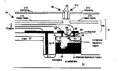
Fi~ures 2A and 2B depict a sensor 50 impiemented as a semiconductor field effect device,
such as an FET. Device 50 may be fabricated in a variety of confi~urations, includin~ a
3 10 junction FET l"JFET"~, a metal-oxide-silicon FET ~"MOSFET"~, a metal-insulator-silicon FET
~"MISFET"), an exposed insulator FET I~EIFET"), an ion sensitive FET (~ISFET"), a distributed
channel bipolar device l"DCBD~), a heterojunction device and a capacitor. Further,
semiconductor device 50 may be operated in enhancement mode, depletion mode, or inversion
mode. It is siQnificant to note that no reference electrode is depicted or required accordin~ to
the present invention.
Device 50 includes a semiconductor substrate bulk 51 havin~ a source 53, a drain 55, an FET
channel 56 capable of electrical conduction, ~n insulation layer 58 such as SiO2, Si3N4, etc.,
an exposed insulator top~ate 60, and a bottom or lower ~ate 62. Accordin~ to the present
invention, the conductivity of channel 56 may be modulated by electrical si~nals and/or char~e
present at top~ate 60 and/or bottom ~ate 62. Preferably device 50 is an expose~ insulator
FET, or "EIFET", with a relatively deep channel 56 lunder no back~ate bbs) to increase device
detection sensitivity.
The uppermost surface 59 of insulator layu 58 is preferably covered with a protective moisture
blocking film 90 that is relatively inert chemicslly, impervious to any corrosive components in
solu~ion 52, will not contaminate the test solution, and provides an outer surface with many
sites for bindin~ with target specific rflcèptor substances 66. Applir ant has found parlyene to
function especially well as film 90, althou~h other materials could also be used. Further, this
structure allows the topQate to float at the potential of the test solution, thus avoidin~ a
top~ate bias that could influence the bindin~ reactions at the top~ate and introduce erroneous
si~nals. As a result, the surface of film 90 can be made selectively reactive without
contamination risk.
Applicant's depletion mode EIFET device IFi~ures 2A and 2B) had a 92.5 nm thickness for
layer 58, an approximately 100 nm parylene film layer 90, an n-epitaxial layer channel 56 with
93~08464 2 1 2 1 7 9 7 PCl/US92/08940
_g _
4.6 microns thickness, doped at about 1 015/cc Icalculated to be 3.4 rnicrons absent back bias),
with WIL ~ 1432 and source-drain dis~ance L= 20 microns. As shown by Fi~ure 2A, the ~ate
60 was fabricated with a meanderline pattern to provide a lar~e W/L usin~ the laboratory
equipment at hand, to thus enhance device sensitivity. In Fi~ure 2A, back~ate 62 is the pn
:~ 5 junction between substrate 51 (p material) and channel 56 ~n-epi re~ion 57~. Of course other
polarity dopants could be used.
, _.
It was not feasible to fully deplete throu~h the device channel due to leaka~e current
~eneration problems associated with the prototype. However, even with partial depletion of
the epi che ~nel, lar~e receptor and tar~et attachment si~nals were observed. These si~nals
10 would be even lar~er for the near total channel depletion condition, 1 ~ drain-sour~e
dimensions Ithus increasin~ W/L) that a commercially fabricated device should produce. A
commercially fabricated device would further permit very hi~h back~ate amplifiration, with
further sensitivity enhancement.
Accordin~ to the present invention, attached char~e influences an underlying channel re~ion
15 in a measurable fashion. It is therefore desired that rec¢ptors 66 be affixed to the present
invention 50 over the top~ate re~ion 60, but not elsewhere. In a conventional inte~rated
circuit, the overlying field oxide layer is of no use in protectin~ underlyinp re~ions apainst
attached surface cl:ar~e. ~Ith reference to Fi~ure 2B, selective receptor attachment can occur
in several ways. In a first method, the uppermost sutfsce of device 50 is masked with an inert
20 a~ent or blockinp a0ent 210 that blocks attachment to material 66 such that only the re~ion
212 over the topgate 60 remains unmasked and thus receptive. The device is then exposed
to a solution containin~ the desired receptor material 66, which attaches over the top~ate
re~ion 212, but not elsewhere due to ~he blockin~ material mask 210.
Alternatively, mask 210 may be a pr~selected blockin~ chemical with a predetermined char~e
25 polarity, chosen such that underlyino r~gions (e.~., devices or circuits) are not unduly
influenced by char~e attached to mask surface 210. Where a specific masking chemical byer
210 has been patterned to protect underlyin~ reoions, post tar~et attachment treatment can
be used, such as preparation with a buffered pH solution correspondin~ to the layer 210's
isoelectronic point.
,
In a second method, the device includes m0talization patterns 214 that preferably shield all of
the device save for the desired top~ate re~ion 212. Preferably the metal mask 214 is covered
by a layer of a material 90, e.~. parylene, to minimi2e possible test solution contamination by
the mask. The device is then exposed to a solution containin~ the desired receptor material
66. Receptors 66 attachin~ over the top~ate re~ion 212 will be in field communication with
the underlyin~ channel re~ion 56, whereas receptors attachin~ elsewhere will have their char~e
, _.~. ,.,., ~ ,. . ...
WO 93/08464 ~ 1 2 1 7 ~ 7 PCr/US92/089~
--10--
~and indeed any subsequently attached tar~et material char~e) shielded from intluencin~
re~ions outside of the top~ate re~ion 212 by the metal mask 214, which is coupled to a DC
potential or ~round.
~ . ,
The potential is selected so underlyin~ re~ions are not unduly influenced by char~e carryin~
~,i 5 chemicals attached above the shield re~ion 214. Thus, shieldin0, includin~ buried metal
;` rnaskin~, is especially desired where the substrate 51 includes o~fier components, such as
. depicted in Fi~ure 5. But for the desired shieldin~ action provided by the mask 214,
performance of other components (e.~., 100, 102, 104) disposed beneath receptor material
66 could undesirably be influenced ~y the resultant electric field chan~es produced by ~he
,10 receptors and/or any tar~ets attached thereto.
A selected primaty receptor 66 is selectively attached to the outer surface of film 90, durin~
or after fabrication of device 50. Essentially primary receptor 66 dedicates device 50 to
'~I bindin~ly detectin~ a matin~ tar~et substance 64, but not other substances 68, 70, 72 that
may be present in the solution ~see Fi~ures 3A, 3B), which other substances may include
char~ed materials and positive and ne~ative ions. As depicted in Fi~ures 5A and 5B, device
50 may in fact include two or more receptor types 66, 6~3', each of which is dedicated to bind
with a different tar~et material.
Alternatively, where simultaneous testin~ for multiple target materials is desired, an array of
sensors incorporatina one or more specific receptors, may be used ~see Fi~ure 5l. Such sensor
arrays may be prepared for sensin~ multiple tar~et substances usin~ photo-patternin~ known
to those skilled in the relevant art. An additional advanta~e of an embodiment such as Fi~ure
5 is that degradation of device sensitivity due to lon~ lead and contact resistance can be
j~ reduced by inte~ratin~ associated circuitry 1100, 102, 104j on a common substrate with on-
chip interconnects. Such on-chip interconnects further minimize test solution contamination
associated with iead contacts and electrodes.
While ~enerally the particle or, target substance, 64 will be a chemical or biochemical, the
I present invention can also test for the presence of photons, the eftects of force, ma~netic
fields, electric fields, and the like. As used herein, ~chemicals" includes not only solutions,
molecules, ions, and atoms, but also subatomic particles, such as electrons. As used herein,
rbiochemicals~ includes not only biochemical compounds such as su~ars, fats, proteins, etc.
but also polymers such as proteins, nucleic acids, ~Iycosamino~lycans, and the like, and
encompasses microorsanisms and fraGments thereof, such as bactorb, viruses, and protozoa
... .. . . ... . . .
WO 93/08'~64 2 1 2 1 7 ~ 7 PCI'/US92/08940
With reference to Figure 2B, preferably, applicant~s depletion mode EIFET structure includes
a li~htly doped n-epi layer 57 te.~., the built-in channel) fabricated on a low resistivity p
substrate 51, wherein N + regions 53, 55 form the device ~ource and drain re~ions. The ~ate
.~' 60 structure is somewhat similar to a JFET with a MOS 0ate, but without rne~alization. Like
a JFET, the device has a built-in channel 56 that, operating in depletion mode, is normally on,
~rl with the depth of the built-in channel land thus channel conductance~ controllable via a reverse
bias coupled between source 53 and substrate 51.
While the present device 50 provides ~ood sensitivity, sensitivity enhancement strcutres can
provide yet additional sensitivity. Typically the top~ate bias causes depletion or accumulation
of the channei re~ion 56 immediateh~ under the top~ate 60. ~AIternatively, if the device 50
^, incorporates an inversinn c hannel, top~ate bias influences the extent of the inversion, e.~.,
channel conductance.) The back~ate is preferably reverse biased to permit the device to
; 1 operate in a hi~hly sensitive re~ime under pre-attachrnent conditions. A relatively small chan~e
,' in a ~ate attached char~e modulates channel depletion width 56 and channel conductance.
This c ondition also requires the lar~est restoration back~ate potential 74, 234 ~Figures 3A, 6A)
to reset the device 50 ts the pre-attachment condition.
,3
~^~ With reference to Fi~ures 3A and 6A, preferably a device accordln~ to the present Inventlon
ulses back~ate bias 74, 234 to restore device operatin~ characteristics to a preattachment
3 condition, where a device operatin~ parameter is selected as a reference value. For example,
the reference parameter ran bé source-drain current, pinch-off volta~e, transconductance
characterized by AC si~nals, source-drain volta~e for constant source-drain current, etc.
~.~
In this operation mode, the device back~ate 62, 270 is biased to restore the preattachment
reference characteristic. Thus if attachment increases channel depletion 62, 271 in the
- depletion mode, a preattachment reverse back~ate bias would require reduction to restore
preattachment operatin~ drain current, where source-drain volta~e was held constant. The
shift in back~ate bias to restore the preattachment condition provides a measure of attach-
ment. In depletion mode operation, the back~ate volta~e preferably slmost pinches off the
channel 56 before attachment ot char~e to the top~ate. This bias re~ime permits the lar~est
percenta~e chan~e of channel resistance and current to be determined, and advanta~eously
requires the lar~est restorin~ back bias volta~e.
,
The use of a measurable back~ate bias to a restore preattachment condition permits
automation usin~ circuits and components known to those skilled in the relevant art. For
example, a volta~e divider providin~ a controllable output volta~e coupled to the backgate
cauld be used with a simple feedback circuit 240 to reestablish drain-source current, the
amount of restoration voltage providing a measure of the attachment condition.
,1~
, , . . ~. . -. , - ~ -
.WO 93/08464 2 1 2 1 7 9 7 PCI'/US92/0894~
--12--
A reference pulsed drain-source current 240 could also be maintained with a pulsed back~ate
: volta~e 234. The resultant pulsed current could be detected and used to adjust, via feedback,
. ~j
the pulsed back~ate volta~e to restore the current ~o the pre-attachrnent value. Alternatively,
a pulsed AC drain-source current dependent upon device transconductance could be used. The
.~ 5 use of AC si~nals such as time dependent back~ate pulse volta~es advanta~eously permits DC
blockin~ capacitors 27 to be used, AC amplification 212 to be incorporated free from DC drift
!~. influences, and allowin~ AC filters to rsject noise to enhance devic~ sensitivity.
. ', .
Sensitivity enhancement is attained because for PN junctions ~e.~., a backE~ate pn junction
270, or a reverse biased channel-substrate 270), the amount of depletion resultin~ from a small
10 reverse bias volta~e chanse is ~enerally dependent upon the initial reverse volta~e ma~nitude.
~' For example, tor a one-sided abrupt junction whose n-side is doped at 1 0t5/cm3, the depletion
'~ width is approximately 5 ,um at 20 V reverse bias, and is about 6 ~m at 40 V reverse bias. It
is this nonlinearity that may be used to increase measurement sensitivity in a device employing
a suitabie back~ate.
Thus, substantially reverse biasin~ the back~ate requires a relatively larQe incremental chanpe
in reverse bias ~compared to an initial lower reverse bias potential) to provide a ~iven chan~e
; in depletion width necessary to reset or reestablish preattachment channel conductance.
Where source-drain output currsnt is to be maintained, the back~ate potential is modulated to
restore the conducting channel to 8 preattachment conductance. Whether an increase or
20 deerease in back~ate reverse bias 74, 234 is rqquired will Jepend on whether attachment
3 increases or decreases depletion or accumulation beneath the ~ate re~ion 60. The ma~nitude
,¦ of volta~e chan~e 74, 234 to restore preattachment channel condition increases with
: increasin~ initial backnate bias, thus enhancin~ device detection sensitivity to attachment.
If this incremental backgate bias chan~e 74, 234 is then coupled to the ~ate of another FET
25 device ~FET 2), a much lar~er output si~nal 212 is available from FET 2 than would have
. initially been present in the first device 50 due to attachment induced conductance modulation
effects. In this fashion, device attachment sensitivity is increased. If the back~ate 62, 270
. is operated in AC pulsed mode, AC amplifiration ot the si~nal delivered to the second device
can yet turther enhance sensitivity.
30 Device 50 can be desi~ned to enhance sensitivity by selection of dopant and dopin~ protiles
. for the pn junction cornprisin~ the back~ate re~ion 62, 270. Where both re~ions are
homo~eneously doped, depletion extent will be the same on either side of the junction. If
however one re~ion 273 is more heavily doped than side 274, then 273's side side will
experience a shallower depletion extent, depletion bein~ inversely proportional to the
35 homo~eneous dopin~ ratio. For example, if the junction's n side is 10~4 more heavily doped
'~3
. ~V~ 93/08464 2 3 2 ~ 7 9 7 P(~/US92/08940
--13--
than the p side, applyin~ a ~iven incremental reverse backaate bias results in about 104 of the
q incremen 3ias fallin~ across, and modulatin~, the n re~ion. Statsd differently, a substantially
,'!~,~ lar~er incremental volta~e must be applied to the back0ate 62, 270 to restore a preattachment
state than would be the case it the two sides of the junction were equally doped. In essence,
5 the two sides ot the pn junction perforrn a volta~e division function, providin~ a small fraction
~, of the total back0ate bias chan~e to the channel side o~ the back~ate junction. Non-linear
junction dopin~ can a~so enhance this desirable sensitivity enhancem~nt fea~ure of a back~ate,
;, accordin~ to the present invention.
~,i
,,.
Other back ~ate junctions may be used with the present invention to enhance tar~et detection
;l 10 sensitivity. A P-l-N back~ate substantially enhances sensitivity usin~ a lar~e intrinsic re~ion,
'~ and droppin~ a lar~e fraction of applied back~ate restorin~ potential across the I re~ion. Thus,
,~ a very srnall fraetion of the back~ate bias modulates the n-channel width, leadin~ to especially
lar~e sensitivity enhancement.
',
Fi~ure 3A depicts a first preferred ~wet" measurement embodiment wherein a device 50
15 contacts a test solution 52 within a container 54, such as a microtiter plate. In operation, film
90 and receptor 66 portion of device 50 are exposed to the test solution 52, allowin~ any
tar~et substance 64 present to bind or attach. Because substance 64 has an associated
electrioal char~e, post-attachment electrical char~es will be present at receptors 66 that can
~-~ affect the performance of device 50.
;~ 20 As noted, semicon~uctor device 50 will ~enerally include at teast one field effect re~ion
wherein the conductivity of a channel 56 is modulated is response to ¢lectrical or char~e activi-
ty on one or more ~ates 60, 62. Such char~e (from bound tar~et 64, for example) creates an
electric field that operates throu~h the thickness ~t of a typically dielectric insulatin~ layer 58
~e.~., SiO2) and terminates on char~es within the semiconductor, ~hareby alterin~ the
25 semiconductor channel reaion 56. The ma~nitude and quantity of such bound charqes alters
the resistance of the conductinD channel.
Alternatively, the device may not emplo~ a conductin~ channel. A sensor field effect device
could be implemented 8s a capacitor device that senses chemical associated char~e
anachment by modulatin~ capacitance chan~e, which change could be sensed by includin~ the
30 capacitor in an appropriate electronic circuit, an RC oscillator, for example.
For a field effect transistor l"FET") device, the resultant electric field modulation of the channel
conductance ~nr resistance) alters the typically drain-source current flow in the channel.
Char0e bindin~ thus alters one or more otherwise quiescent characteristics of device 50, which
alteration may be sensed and measured, qualitatively and/or quantitatively, usin~ equipment
: ` WO 93/08464 2 1 2 1 7 9 7 P~/US92~08940
--14--
70. The rneasurable characteristics may include, without limitation, drain current, chan~e in
, ! threshold volta~e, pinchoff volta~e, ~ate-source volta~e, transconductance, conductance, ~ate-
source capacitance, ~ate to substrate capaci~ance, back gate capacitance, transconductance
threshold volta~e ~DCBI)", and ~ated bipolar devices), bipolar current ~ain (DCBD),
5 transconductance ~DCBD), and chan~e in source volta~e ~or constant drain current.
For example, the attachment of a tar~et-ori~inatin~ char~e sheet,resO-lts in an associated
electric field ~enerated across a thickness of insulator material, which results in a threshold
3 volta~e shift in an insulator pate field effect device. The resultant incremental threshold
voltage chan~e alters the device's operatin6 characteristics, which characteristics may be used
, 10 to influence an associated circuit to provide an enhanced measurement si~nal representin~
attached char~e. Such measurement may represent, for example, channel resistance,
~'~ switchin~ time, oscillator frequency lwhere the device is incorporated in an oscillator circuit),
` ! channel ~ransconductance, output current into a bipolar transistor base, etc. Further details
regardin~ field effect theory and modellin~ may be found in a number of standard treatises,
15 includinp "Device Electronics for Inte~rated Circuits", 2nd ed., by Muller and Kamins, published
, I by John Wiley.
.~
In the confi~uration ot Fi~ure 3A, attachment measurements are made while device 50 is still
in the solution 52, typically at the time of attachment, or in some other solution (here shown
as 52 also) whose ptl, temperature, chemical composition, etc. may differ from test solution
20 52. As shown, durin~ measurement device 50 is coupled to measurement equipment 70,
which preferably includes one or more measuring instruments 72 such as an oscilloscope,
current probe, semiconductor parameter analyzer or curve tracer, capacitance measurin~
instrument, specially designed instruments sensitive to the sensor parameters of interest, and
the like. Equipment 70 also includes a varbble power source 74 that is preferably coupled to
25 device 50's bottom ~ate 62. Optionaily, cquipment 70 can inciude an additional power source
76, coupled to device 50, for establishing a pre-binding quiescent state.
When a tar~et substance 64 binds to a receptor 66, the associated substance char~e and/or
contact potentbl will alter device 50's conductance state. For example, depending upon the
, mode of device 50, a binding condition can be associated with an increase or decrease in
30 channel conductance, a chan~e in drain current or pinch-off voltage or threshold voltage, a
chan~e in transconductance, in channel width or depletion, and so on. One or more such
characteristic chan~es may be measured by equipment 70 to provide a signal corresponding
to attachment.
Preferably the variable power source 74 is adjusted, post-attachment, to restore whatever pre-
35 attachment quiescent condition existed for device 50. Equipment 70 can measure the amount
_~
WO ~3/08464 2 ~ 9 7 PCr/US92/08940
~. --15--
',;` of restoration bias required from power source 74 to provide an increased measure of the
attachmsnt. The compensatin~ or restoration bias can be amplified, e.~., by ampiifier 78, and
. ~ the amplified si~nal coupled to one or rnore additional components 80. Component 80, in turn,
could include a second device 200, coupled to perform a cascode amplification function upon
-i, S the amplified restora~ion bias sinnal. If desired, the compensation bias si~nal from potential
source 74 may be coupled to a feedback circuit 82 to automatically provide and maintain
ii proper restoration bias Isee also Fi~ures 6A and 6B). The desi0n of-such feedback circuitry
is well known ~o those skilled in the relevant art, and thus detailed information is not here
presented.
, .
With further reterence to Fi~ure 3A, as indicated by capacitor 82, the restorative bias from
potential source 74 could in fact be an AC coupled pulse train, wherein one level corresponds
to rpre-bindin~" and a second level ot the pulse train corresponds to "post-bindin~". Because
~ such pulse train si~nal is AC, capacitor 82 can decouple undesired effects of power source.
;.3 This facil tates AC amplification of the detected si~nal, reducin~ susceptibility to problems
associated with drift in DC amplifiers, power sources, etc. Further, rapacitor 82, coupled in
~3 series with the bottom ~ate 62 as shown, determines the ex~ent an applied AC compensatin~
reverse bias from power source 74 affects device 50's channel conductan~e, or other
operatin~ characteristics. Volta~e division, e.~., with a capacitor voltage div;r-~., can also
provide a "sensed~ volta~e ~ain, wherein a srnall traction of the power source is used as a
2Q restorative potential, with the total power supply potential beinu measured to indicate the
amount of ~ate char~e attachment to be sensed.
The embodiment of Fi~ure 3B is similar to what has been de~cribed except that while bindin~
occurs in solution ~as in Fi~ure 3A), dry measurements are made. In practice, device 50 is
;
exposed to ~he test solution 52 potentially containin~ the tar~et substance 64. It is understood
25 that in this embodiment, equipment 70 need not be present when or where device 50 is
exposed ~o the target substance.
¦ Materials n0eded for measurement enhancement and any confirmational testinQ need not exist
; at the time and place that testin~ occurred lonly at the measurement site). This is
advanta~eous, especially if the testin~-bindina site is in a remote location, or a location not
, ~0 amenable to storin~ enhancement materials under controlled conditions.
Applicant has discovered that such dry rneasurement advanta~eously eliminates the ion
shieldin~ problem so prevalent in the prior art. Accordin~ to the present invention, removin~
the device 50 frorn an ionic solution 8 before testin~ facilitates elimination of the external
reference elec~rode and attendant ~ate bias problems, dritt and potential chemical
35 contamination so prevalent in the prior art. In the present invention, attached surface char~e
is sensed directly.
,~
WO 93/O~ 2 1 7 9 7 PCI`/VS92/08940
. --16--
Once a sensor 50 with bound tar~e~ matter 64 is remo~ed from an ionic test solution 52, the
char~es associated with the bound matter are no lon~er shielded by ions in the no lon~er
present solution. As a result, a net char~e is manifested at layer 60 generatin~ an associated
electric field across the underlying insulator layer 58. This char~e and the attendant electric
; 5 field attract oppositely charged free carrier char~es from the semiconductor substrate 56 ~or
repel like polarity free carrier charyes), resultin~ in opposite charges at or near the surface of
, ~he substrate 56. It is ~o be noted that ~he effects of contact poten~ia~at the sensor ~ate are
- ~eneraily different than the effects of bound charges.
Contact potential and char~e attachment influences on a sensor, arising from tar~et material
10 attachment, may be separated by comparin~ the influence of target material attachment on the
top~ate re~ion 66 of two sensor devices 50, 50' identical except for their insulator thickness
91. Separatin~ the effects of these two phenomena occurs because while the attached charge
~enerates an electric field across an insulator independent of insulator thickness, the contact
potential induced electric field is inversely dependent upon insulator thickness. Thus, makin~
15 two independent measurements of two unknowns permits identifyin~ charge attachment
effects, and contact potential eftects upon sensor device 50.
Where the desired information is a direct measurement of tar~et material concentration, binding
rate of the tar~et material to a receptor, dissociation rate, binding ener~y, etc., the test may
be interrupted before steady state is achieved.
,1
20 Accordin~ to a pleferred embodiment depicted in Fi~ure 5, substrate 56 can include an on-chip
pH sensor 100 and stora~e mechanism 102 for memorializinn the test solution's pH value. The
on-chip pH sensor 100 itself may be implemented as a device, according to the present
invention, and may include the various enhancement techniques described herein.
Further, various confirmational devices, devices for measuring cofactors, and devices for
25 measurin~ other chemicals of interest and for measurin~ chip receptor condition and integrity
can be included on the same semiconductor chip. Preferably the sensor system further
includes an on-chip mechanism 104 for measuring and storin~ the pre-attachment quiescent
conditions of one or more devices ~e.~., 50A, 50B, etc.) Sabricated on the same substrate. For
ease of illustration, Fiaure 5 does not depict the couplinas between device 104 and the various
3() sensors.
As depicted by Fiaure 5, the sensor system 106 can include measurement circuitry, e.g., 104,
for each sensor device, and circuitry providino error alerts where, for example, receptor
inte~rity, storage conditions, etc., are in question. Such on-chip circuitry can include a
temperature sensor to monitor incubation conditions present during the chemical reaction of
' WO 93/08464 2 1 2 1 ~ 9 7 PCr/USg2/0894~
,
--17--
.. ; .
interest (including attaehment and dissociation), as well as a clock measurin~ reaction or
dissociation prociss times. Thus, system 106 can measure physicai parameters includina
reaction temperature, reaction time, solution pH, and ionic conc~ntration.
~'
In the ~eneralized embodiment of Fi~ure 5, note that it is not necessary that each sensor be
. .
5 identical, either in size, or in the densit~ and/or number of receptor types 66, 66~. For
example, sensor 50F includes no receptors and may be coated with'anrnert material, and may
; ~ be used as a calibration sensor in that the ~betore~ and ~after" bindin~ characteristics of sensor
. .,
i~JI 50F should be the same. Confirmational testin~ excludin0 a non-specific reaction with device
il
50F's inert meterial could be achieved by providin~ another sensor whose outer film should
10 also be non-reactive with the test solution contents. ~Before~ bindin~ data from sensor 50F
may be stored in device 104 for comparison to the sensor's "after~ bindin~ data. If the two
~; sets of data do not a~ree, a user would know to suspect the inte~rity of data from sensors
50A-50E. For example, the array 106 of sensors may have been dama~ed at some time.
;~
The ernbodiment of Figure 5 also promotes confirmatory testin~ not merely of the devices
15 themselves, but of various tar~et materials. For example, device 50B has a ~reater density of
the same type of receptors than does device 50A. Therefore confirmation of bindin~ the
appropriate taraet material for receptors 66 would be indicated by a proportionally ~reater
bindin~ effect upon device 50B contrasted with device 50A.
Further, by providin~ some devices with only a first type of receptor le.~., device 50A), and
20 some devices with only a second type of receptor (e.a., device 50C), a differential analysis of
a bindin~ event may be made. For example, a tar~et substance suitable for bindin~ only with
receptors 66 should produce a measurable chande in device 50A, but not in device 50C.
Further, a device such as dovice SOE may include both sensor types to provide still further
confirmatory information as to thç nature of what the bindinq substance is. Additional
25 confirmatiQnal data may be acquired by re-exposure of a previously exposed test device to a
different temperature, different pH, differont chemicals, etc., providin~ known results for the
tar~et material. For example, dissssociation rate of nucleic acid components with
temperature, dissociation with pH chan~e, char~e chan~e with pH chan~e, char~e si~n chan~e
, with pH chan~e, disassociation as a function of different receptor bindin~ sites, etc., provide
30 useful informa~ion, especially as to whether what bound to the receptor of interest was in fact
the desired tar~et material.
Differential anal~sis could also be performed by exposin~ two identical sensors to a tar~et
material for two different time len~ths, each shorter than the time known to be required for the
tar~e~-receptor reaction to complete. Char~e measurement for each device provides dsta for
`: W0 93/08464 2 1 2 1 7 ~ 7 PCr/US92/08940
.. . . .
--18--
tar8et material reaction lor attachment) rate, and concentration in the test solution, data useful
:` to provide species identification.
Whether measurements are conducted wet las depicted in Fi~ure 3A1 or dry/quasi-dry ~as
depicted in Fi~ure 3B~, the bound char~es result in an elactric field that can modulate the
5 conductance of the device semiconductor channel ~if not neutralized by shieldin~, etc.). This
modulation permits detection usin~ suitable equipment 70, accordin~toth2 present invention.
While the description thus far has been with respect to a sensor 50 such as depicted in Fi~ures
3A and 3B, accordin~ to the present invention, o~her semiconductor field effect sensors
. .~
includin~ the embodiment of Fi~ure 4 ~and devices functionaliy similar thereto) could also be
10 used.
.,1
;:~ The present invention also facilitates obtainin~ sequence information of polymeric molecules
f,.~ such as DNA, RNA, ~Iycoconju~ates, polypeptides, and so forth. Another preferred sensor
ernbodiment that is very well suited for detectin~ binding attachment in a sensor application
,,1 is depicted in Fi~ure 4. Device 50~ is a so-called distributed channel bipolar device (~DCBD"),
15 similar to what is disclosed in U.S. Patent No. 4,885,623 to James Holm-Kennedy, et. al.
1989). The DCBD structure of device 50' includes FET components gate oxide insulation
layer 58~! an appropriate moisture biockin~ layer 90', ~ate 60', drain 100, channel re~ion 56',
as well as bipolar cornponents base 104 and emitter 106. While Fi~ure 4 depicts a DCBD
device with vertical architecture, alternatively, a DCBD device could be fabricated with bteral
25) architecture, or a combination of vertical and lateral architecture. Similar to what was set forth
above with refer~nce to device 60 of Figures 3A and 3B, in sensor applications, the pate 60'
supports an moisture blocktng protective film 90' to whose outer surface primary receptors 66'
are attached.
As described in detail in said U.S. Patent No. 4,885,623, dependin~ upon mode of operation,
25 the DCBD may be treated as an FET device with a bipolar sourc~ or drain that may be distrib-
uted. The DCBD may also be treated as a bipolar device with an FET emitter or collector that
may be distributed, or as a ~ated bipolar device. The DCBD may be operated in enhanced or
depletion mode. Further, vertical and lateral bipolar devices can be incorporated in a DC8D
device. The FET portion of a DCBD device may incorporate a MESFET, JFET, or IGFET
30 structure.
DCBD devices are especiallY well suited for sensor wet and dry testin~, accordin~ to the
present invention. DCBD devices exhibit hi~h transconductance and current ~ain sensitivity
to relatively small chan~es in ~ate volta~e or char~e, resultin~ from the bindin~ of a taroet
substance to the device. DCBD devices are also very sensitive to small chan~es in base
35 curren~, under certain operatin~ conditions. Further, techniques may be employed to enhance
WO 93/û~464 2 ~ 2 1 7 9 7 P~/US92/08940
. .
--19--
various DCBD ,oarameters in response to tar~et binding. Such enhanceable parameters include
bipolar ~ain, ~at~ and base current dependent current Uain, hetero~eneous channel behavior,
effective gate area and ~ate shape, and transconductance threshold volta~e effect.
Transconductance measurements with device 50' are especially advanta~eous because a null
5 may be detected usin~ alternatin~ current ~"AC"~ ampiifiers, operatin~ at hi~h ~ain.
Electrophoresis applications are also applicable to sensor devices such as the present invention .
~! With reference to Fi~ures 6A and 6B, two embodiments of feedback for sensor reset and
~i~i sensitivity enhancement measurement approaches are shown. In Fi~ure 6A, sensor 50 is
: .1
., biased by a pulsed back~ate bias supply 234, to reset or restore device 50 to its preattachment
~, 10 condition, while measurement system 230 monitors a device operating parameter sensitive to
i char~ed tar~et attachment. For ease of illustration, parameter measurement system 230 is
indicated ~enerally, without a specific coupling 232 to the device to illustrate that the chosen
~,1 parameter(s) may be varied, and can include current, voltage, transconductance, etc. The
j sensed parameter provides a feedback signal to feedback system 240 ~hat, in response, adjusts
the back~ate operating voltage to restore the preattachment conditions.
'`'1
In Fi~ure 6A, the reset voltape from supply 234 is coupled to the input of a second device, FET
2, selected for hi~h aain le.~., a thin ~ate oxide device). In this cascode circuit, output current
Id 212 from sensor device 50 is amplified by FET 2, whose FET 2 output may be used to de~ect
, the target attachment event. Further, this output si~nal 212 may be processed with circuit
214 to provide additional information, and/or may be coupled to a feedback circuit 240 Ishown
in phantom) for restorin~ preattachmsnt device 50 conditions. If desired, FET 2 may be a
: - component in a circuit whose performance is affected by FET 2's change in channel resistance
respondin~ to attacned char~e at device 50. For example, if FET 2 affects the frequency of
an oscillator 210, attachment at device 50 may be sensed by monitoring frequency change at
oscillatcr 210.
. In Fi~ure 6B, a constant current is maintained in device 50, whereupon a certain voltage is
: seen across device back~ate 270. Char~e attaching to the top~ate 272 of device 50 will
induce a backgate volt3~e chan0e, which chanae provides a measure of the attached char~e.
, The current Id may be AC pulsed, which allows AC amplification 237 without problems
associated with DC amplifier drift.
In this example, the net charge upon device 50 from target 64 has been increased, including
char~e effects from the additional attachment of receptors to the "sandwich~ . Numerous other
means of enhancing or amplifyin~ the si~nal generated by target binding are available to those
skilled in the relevant art. For example, as depicted in the rioht-hand portion of Figure 7B, a
con~lomerate may be used in the third sequence, wherein device 50 could be exposed to
material havin~ substantially more charge than target 64. For example, such material might
WO 93~0&~64 2 ~ 2 :1 7 9 7 PCI`/US92/08940
--20--
include a DNA chain ~or fra~ment) 112 attached to a tar~et substance 64X that will bind to
the receptor 66X. In this tashion, a subs~antially lar~er net charpe attaches to the field effect
sensor device, resultin0 in a lar~er si~nal. It is understood that char~e associated with receptor
66 and tar~et 64 may be additive or subtractive, as may also be the case with material 66X,
. 5 64X and 112.
. ~ . .
~l Fi~ure 7C depicts the use of beads as an alternativ& lor additio,nalt--method of passively
.. ;, enhancing device sensitivity. Beads 114 may have a variety of shapes, are commercially
., available in sizes ran~in~ from about 0.1~ to several ~1, and are ~lass or polymer, e.~., materials
'~, affordin~ many bindin~ sites for a plurality of secondary receptors 66'. Receptors 66' have
10 similar selective reactivity characteristics as the primary receptors 66, and may in fact be
:~ identical thereto. Beads, like conjugates, are commercially available and are frequently made
from ~old, biotin, ferritin, and the like, and may be made from other chemicals such as nucleic
.~ acid chains and antibody chains. In a second sequence, after tar0et 64 has bound to primary
receptor 66, the device 50 is exposed to a typical solution containin~ conjugated receptors
~j 15 116.
. With reference ~o Fi~ures 8A-8C, the drain cu~rent ~Ids~ and drain-source volta~e (Vds) for
. sensor 50 was measured after the application of various biolayers. For the data shown in
`~1 these fi~ures, incubation was 27C with a 1ûmM MOPS buffer employed to maintain pH ~
~3 7. With reference to Fi~ure 8B, for example, the device was tested before and after
20 application of a parylene film 90 Ibar ~raphs a and b~. After stabilizin~ the device in a MOPS
buffer solution measurement~ were aqain taken (bar qraph c). A receptor layer Ireceptor:l~G)
was applied, and measurements taken Ibar ~raph dt, after which the device was exposed to
a BSA blockin~ a~ent and measured ~bar ~raph e~. The utility of the BSA blocking layer is
shown by bar ~raph f IFi~ure 8B), wherein the device was exposed to a non-specific antibody.
25 As shown by bar ~raphs e and f, there was relatively little chan~e in char~e from non-specific
bindin~s, which indicates BSA suppression of non-specific bindin~. Next the device was
exposed to a desired tarGet substance (anti~en: Goat anti-l~G), and a chan~e in char~e (~Q)
, was noted (bar ~raph ~). Finally, the device was reexposed to receptor material (l~i), which
resulted in essentially the same charge change (AQ). It is noted from Fi~ures 8B and 8C that
, 30 different chemical exposure and reactions can result in char~e attachment of different
polarities, as indicated by the direction of the bar shift after exposure to subsequent chemical
exposure .
The data for bar ~raph a in Fioure 8C depicts a denatured device 50. After denaturina, the
device was exposed to a buffered MOPS solution Ibar ~raph b), which altered the effective
35 char~e on the device. Thereafter in a suitable incubation environment, receptors were attached
~bar ~raph c), which in this case altered the ~ate attached char~e. Exposure to a BSA
WO 93/0&~64 2 1 2 1 7 9 7 Pcr/usgt/o894o
--21--
environrnent ~bar ~raph d) sli~htly chan~ed the char~e, and exposure to the tar~et material ~bar
~raph f~ resulted in a desired perceptible char~e chan~e l\Q.
Automated testin~ is readily implemented usinç the invention, which can include on-chip
testin~ circuitry ~see Fi~ure 5). Dry ~estin~ particularly promotes automated procedures, where
r 5 the bound sensors may be automatically delivered to a test fixture (e.~., a test probe), where
~-~ test information is read and the test results stored for au~omatic cgmputer processin~.
.- While the present invention has been described with reference to a few specific embodiments,
the description is illustrative of the invention and is not to be construed as limitina the
invention. Various modifications may occur to those skilled in the art without departin~ from
the true spirit and scope of the invention as defined by the appended claims. 4
,.,
.1
i
~' ' .