Note: Descriptions are shown in the official language in which they were submitted.
_ 21222'4
_1_
LIQUID CRYSTAL DISPLAY APPARATUS AND DRIVE METHOD
FIELD OF THE INVENTION AND RELATED ART
The present invention relates to a liquid
crystal apparatus suitably used as a display apparatus
for computer terminals, television receivers, word
processors, typewriters, etc., inclusive of a light
valve for projectors, a view finder for video camera
recorders, etc., particularly such a liquid crystal
?0 apparatus using a ferroelectric liquid crystal
(hereinafter sometimes abbreviated as "FLC") and a
driving method therefor.
Clark and Lagerwall have disclosed a bistable
FLC device using a surface-stabilized ferroelectric
liquid crystal in, e.g., Applied Physics Letters, Vol.
36, No. 11 tJune 1, 1984), p.p. 899 - 901; Japanese
Laid-Open Patent Application ~JP-A) 56-107216, U.S.
Patent Nos. 4,367,924 and 4,563,059. Such a bistable
ferroelectric liquid crystal device has been realized
2Q by disposing a liquid crystal between a pair of
substrates disposed with a spacing small enough to
suppress the formation of a helical structure inherent
to liquid crystal molecules in chiral smectic C phase
(SmC'~} or H phase (SmH~} of bulk state and align
vertical (smectic) molecular layers each comprising a
plurality of liquid crystal molecules in one
direction.
21222'4
-2-
Further, as a display device using such a
ferroelectric liquid crystal (FLC), there is known one
wherein a pair of transparent substrates respectively
having thereon a transparent electrode and subjected
to an aligning treatment are disposed to be apposite
to each other with a cell gap of about 1 - 3 um
therebetween so that their transparent electrodes are
disposed on the inner sides to form a blank cell,
which is ther_ filled with a ferroelectric liquid
crystal, as disclosed in U.S. Patent No. 4,639,0$9;
4,655,561; and 4,681,404.
The above-type of liquid crystal display
device using a ferroelectric liquid crystal has two
advantages. One is that a ferroelectric liquid
crystal has a spontaneous polarization so that a
coupling force between the spontaneous polarization
and ar_ external electric field can be utilized for
switching. Another is that the long axis direction of
a ferroelectric liquid crystal molecule corresponds to
2~ the direction of the spontaneous polarization in a
one-to-or_e relationship so that the sv~:itching is
effected by the polarity of the external electric
field. More specifically, the ferroelectric liquid
crystal in its chiral smectic phase show bistability,
i.e., a property of assuming either one of a first and
a second optically stable state depending on the
polarity of an applied voltage and maintaining the
212227
-3-
resultant state in the absence of an electric field.
Further, the ferroelectric liquid crystal shows a
quick response to a change in applied electric field.
Accordingly, the device is expected to be widely used
in the field of e.g., a high-speed and memory-type
display apparatus.
A ferroelectric liquid crystal generally
comprises a chiral smectic liquid crystal (SmC'~ or
SmH'~), of which molecular long axes form helixes in
1Q the bulk state of the liquid crystal. if the chiral
smectic liquid crystal is disposed within a cell
having a small gap of about 1 - 3 ~: as described
above, the helixes of liquid crystal molecular long
axes are unwo~.:nd ~N.A. Clark, et al., MCLC (1983),
~5 Zlol. 94, p.p. 213 - 234).
A liquid crystal display apparatus having a
display panel constituted by such a ferroelectric
liquid crystal device may be driven by a multiplexing
drive scheme as described in U.S. Patent No.
2p 4,55~,~~1, isslzed to Kanbe et al to form a picture
with a large capacity of pixels. The liquid crystal
display apparatus may be utilized for constituting a
display panel suitable for, e.g., a cWOrd processor, a
personal computer, a micro-printer, and a television
2~ set .
A ferroelectric liquid crystal has been
principally used in a binary (bright-dark; display
212274
device in which two stable states of the liquid
crystal are used as a light-transmitting state and a
light-interrupting state but can be used to effect a
mufti-value display, i.e., a halftone display. In a
halftone display method, the cereal ratio between
bistable states (light transmitting state and light-
interrupting state) within a pixel is controlled to
realize an intermediate light-transmitting state. The
gradational display method of this type (hereinafter
y referred to as an "cereal modulation" method) will now
be described in detail.
Figure 1 is a graph schematically
representing a relationship between a transmitted
light quantity I through a ferroelectric liquid
crystal cell and a switching pulse voltage tl. More
specifically, Figure lA shows plots of transmitted
light quantities I given by a pixel versus voltages V
when the pixel initially placed in a complete light-
interrupting (dark) state is supplied cFith single
2~ pulses of various voltages V and one polarity as shown
in Figure 1B. then a pulse voltage V is beloisT
threshold Vth (V < Vth), the transmitted light
quantity does not change and the pixel state is as
shown in Figure 2B which is not different from the
state shown in Figure 2A before the application of the
pulse voltage. If the pulse voltage V exceeds the
threshold Vth ~Vth < V < Vsat), a portion of the pixel
z~zz2~4
-5-
is switched to the other stable state, thus being
transitioned to a pixel state as shown in Figure 2C
showing an intermediate transmitted light quantity as
a whole. If the pulse voltage V is further increased
to exceed a saturation value Vsat (Vsat < V), the
entire pixel is switched to a light-transmitting state
as shown in Figure 2D so that the transmitted light
quantity reaches a constant value (i.e., is
saturated). What is, according to the areal
l~ modulation method, the pulse voltage V applied to a
pixel is controlled within a range of tlth < V < trsat
to display a halftone corresponding to the pulse
voltage.
However, actually, the voltage (V) -
transmitted light quantity (I) relationship shown ir_
Figure 1 depends on the cell thickness and
temperature. Accordingly, if a display panel is
accompanied with an unintended cell thickness
distribution or a temperature distribution, the
2~ display panel can display different gradation levels
in response to a pulse voltage having a constant
voltage.
Figure 3 is a graph for illustrating the
above phenomenon which is a graph shoeing a
?5 relationship between pulse voltage (V) and transmitted
light quantity (I} similar to that shown in Figure 1
but showing two curves including a curve H
21222~~
_s_
representing a relationship at a high temperature and
a curve L at a low temperature. In a display panel
having a large display size, it is rather common that
the panel is accompanied with a temperature
distribution. In such a case, however, even if a
certain halftone level is intended to be displayed by
application of a certain drive voltage Vap, the
resultant halftone levels can be fluctuated within the
range of Il to I2 as shown in Figure 3 within the same
Ip panel, thus failing to provide a uniform gradational
display state.
In order to solve the above-mentioned
problem, our research and development group has
already proposed a drive method (hereinafter referred
to as the four pulse method"} as disclosed in Japanese
Laid-Open Patent Application (JP-A) 4-21$022. In the
four pulse method, as illustrated in Figures 4 and 5,
all pixels having mutually different thresholds on a
common scanning line in a panel are supplied with
2~ plural pulses (corresponding to pulses (A) - (D) in
Figure 4} to sho:~ consequently identical transmitted
quantities as shown at Figure 4(D). In Figure 5, T1,
T2 and Tz denote selection periods set in synchronism
with the pulses (B), (C} and (D), respectively.
Further, Q~, Qn', Q1, Q2 and Q~ in Figure 4 represent
gradation levels of a pixel, inclusive of QQ
representing black (~ °} and Q~' representing white
_.,_
(100 -°s}. Each pixel in Figure 4 is provided with a
threshold distribution within the pixel increasing
from the leftside toward the right side as represented
by a cell thickness increase.
Our research and development group has also
proposed a drive method (a so-called "pixel shift
method", as disclosed in European Patent Appln. 0 545 400,
entitled "LIQUID CRYSTAL DISPLAY APPARATUS"), requiring a
shorter writing time than in the four pulse method. In the
Fixel shift method, plural scanning lines are
simultaneously supplied with different scanning
signals for selection to provide an electric field
intensity distribution spanning the plural scanning
lines, thereby effecting a gradational display.
~5 According to this method, a variation in threshold due
to a temperature variation can be absorbed by shifting
a writing region over plural scanning lines. A
similar concept is also disclosed in JP-A 63-29733.
An outline of the pixel shift method will now
be described below.
A liquid crystal cell (panel) suitably used may be
one having a threshold distribution within one pixel. Such a
liquid crystal cell may for example have a sectional struct-
ure as shown in Figure 6. The cell shown in Figure 6 has an
FLC layer 55 disposed between an upper glass substrate 53a
and a lower glass substrate 53b, the upper substrate 53a
r
_8_
having thereon transparent stripe electrodes 51a consti-
tuting data lines and an alignment film 54a and the lower
substrate 53b having thereon a ripple-shaped film 52 of,
e.g., an insulating resin, providing a saw-teeth shape
cross section, transparent stripe electrodes 51b
constituting scanning lines and an alignment film 54b.
In the liquid crystal cell, the FLC layer 55 between
the electrodes has a gradient in thickness within one
gixel so that the switching threshold of FLC is also
lp caused to have a distribution. When such a pixel is
supglied with an increasing voltage, the pixel is
gradually switched from a smaller thickness portion to
a larger thickness portion.
The switching behavior is illustrated with
reference to Figure 7A. Referring to Figure 7A, a
panel in consideration is assumed to have portions
having temperatures Tl, T2 and T3. The switching
threshold voltage of FLC is lowered at a higher
temperature. Figure 7A shows three curves each
2p representing a relationshig between agglied voltage
and resultant transmittance at temperature Tl, T2 or
T3.
Incidentally, the threshold change can be
caused by a factor other than a temperature change,
25 such as a layer thickness fluctuation, but an
embodiment of the gresent invention will be described
while referring to a threshold change caused by a
a
mz~~~4
temperature change, for convenience of explanation.
As is understood from Figure 7A, when a
pixel at a temperature T1 is supplied with a voltage
Vi, a transmittance of R °s results at the pixel. If,
however, the temperature of the pixel is increased to
T2 or T3, a pixel supplied with the same voltage Vi is
caused to show a transmittance of 100 ~, thus failing
to perform a normal gradational display. Figure 7C
shows inversion states of pixels after writing. Under
such conditions, v,=ritten gradation data is lost due to
a temperature change, so that the panel is applicable
to only a limited use of display device.
In contrast thereto, it becomes possible to
effect a gradational display stable against a
temperature change by display data for one pixel on
two scanning lines S1 and S2 as shown in Figure 7D.
The drive scheme will be described in further
detai 1 hereinbelocs=.
(1) A ferroelectric liquid crystal cell as shown
in Figure 12 having a continuous threshold
distribution within each pixel is provided. It is
also possible to use a cell structure providing a
potential gradient within each pixel as proposed by
our research and development group in TJ.S. Patent No.
4,815,823 or a cell structure having a capacitance
gradient. In any way, by providing a continuous
threshold distribution within each cell, it is
2122274
-10-
possible to form a domain corresponding to a bright
state and a domain corresponding to a dark state in
mixture a=ithin one pixel, so that a gradational
display becomes possible by controlling the areal
ratio between the domains.
The method is applicable to a stepwise
transmittance modulatior_ (e.g., at 16 levels} but a
continuous transmittance modulation is required for an
analog gradational display.
(2) Two scanning lines are selected
simultaneously. The operation is described with
reference to Figure 8. Figure 8A shows an overall
transmittance - applied voltage characteristic for
combined pixels on two scanning lines. In Figure 8A,
a transmittance of 0 - 100 % is allotted to be
displayed by a pixel B on a scanning line 2 and a
transmittance of 100 - 200 % is allotted to be
displayed by a pixel A on a scanning line 1. More
specifically, as one pixel is constituted by one
scanning line, a transmittance of 200 % is displayed
when both the pixels A and B are wholly in a
transparent state by scanning two scanning lines
simultaneously. Herein, t~:o scanr_ing 1 i nes are
selected for displaying one gradation data but a
region having an area of one pixel is allotted to
displaying one gradation data. This is explained with
reference to Fig~~rp 8B.
2122274
_11_
At temperature T1, inputted gradation data is
written in a region corresponding to 0 % at an applied
voltage VO and in a region corresponding to 100 % at
V100- As shown in Figure $B, at temperature Tl, the
range (pixel region) is wholly on the scanning line 2
(as denoted by a hatched region in Figure $B). When
the temperature is raised from Tl to T2, however, the
threshold voltage of the liguid crystal is lowered
correspondingly, the same amplitude of voltage causes
an inversion in a larger region in the pixel than at
temperature Tl.
For correcting the deviation, a pixel region
at temperature T2 is set to span on scanning lines 1
and 2 (a hatched portion at T~ in Figure $B).
~5 Then, when the temperature is further raised
to temperature T~, a pixel region corresponding to an
applied voltage in the range of VO - V100 is set to be
on only the scanning line ? (a hatched portion at T$
in Figure $B).
2Q By shifting the pixel region for a
gradational display on two scanning lines depending on
the temperature, it becomes possible to retain a
normal gradation display in the temperature regior_ of
T1 _ T3.
25 (3) Different scanning signals are applied to the
two scanning lines selected simultaneously. As
described at (2) above, in order to compensate far the
-12-
change in threshold of liquid crystal inversion due to
a temperature range by selecting two scanning lines
simultaneously, it is necessary to apply different
scanning signals to the two selected scanning lines.
This point is explained with reference to Figure 7.
Scanning signals applied to scanning lines 1
and 2 are set so that the threshold of a pixel B on
the scanning line 2 and the threshold of a pixel A on
the scanning line 1 varies continuously. Referring to
Figure 7B, a transmittance-voltage curve at
temperature Tlindicates that a trans~ittance up to 100
is displayed in a region on the scanning line 2 and
a transmittance thereabove~and ug to 200 ~ is
displayed in a region on the scanning line 1. It is
necessary to set the transmittance curve so that it is
continuous and has an equal slope spanning from the
pixel B to the pixel A.
As a result, even if the pixel A on the
scanning line 1 and the pixel B on the scanning line 2
are set to have identical cell shapes as shown in
FIgure 9B, it becomes gossible to effect a display
substantially similar to that in the case where the
pixel A and the pixel B are provided with a continuous
threshold characteristic (cell at the right side of
Figure ?B).
In the above-described known pixel shift
method, pixels on an N-th scanning-line and pixels on
A
212224
-I3-
a preceding and adjacent (N-1)-th scanning line are
written by simultaneously receiving different
selection signals, so that data on the N-th scanning
line is shifted to the (N-1)-th scanning line
corresponding to a threshold change in associated
pixels due to a temperature change, etc., thereby
correcting the threshold change due to a temperature
change, etc.
In such a driving scheme, however, the
IO scanning lines have to be selected consecutively and
line-sequentially, so that the scheme is not
compatible with an interlaced scanning scheme ~s=herein
physically adjacent scanning lines are selected non-
Continuously.
On the other hand, in an FLC device, one
picture-writing time (one frame scanning period)
amounts to 102.8 cosec if it is assumed that one line-
scanning time is 100 usec and one picture is
constituted by 1028 scanning lines. This corresponds
2Q to a dricre frequency of 9.73 H~, i.e., 9.73 times of
picture writing in one second.
if a brightness irregularity on a display
picture is caused as a regular movement, the state is
noticeable as flickering on the picture to human eyes.
In order to remove the flickering, it is required to
raise the dricre frequency to about 40 Hz or adopt an
interlaced scanning (thinning out or jump scanning)
-14-
scheme.
In order to raise the drive frequency to 40
Hz, it is necessary to set the one line-scanning
period to 24 usec in the above-mentioned case of
driving 1028 scanning lines. This is difficult to be
accomplished (A) in view of the presence of a delay in
transmission of an applied voltage waveform along a
liquid crystal panel and (B) if the gradation signal
is constituted by pulse width modulation. Thus, this
is difficult to be applied to a display panel of a
large area and a high resolution.
In order to prevent the flicker by providing
an apparently increased drive frequency, a method of
applying a so-called dummy scanning signal has been
proposed by our research and development group as
disclosed in JP-A 4-105285
However, this method is accompanied with a difficulty
that a decrease in contrast is inevitably caused.
Several interlaced scanning schemes are
present in order to prevent the flicker. Among these,
it is most desirable to use a scheme wherein the
interlacing is performed at a weak regularity. For
example, a first scanning line is first selected and
subsequent scanning is performed with skipping of 8
lines in a first vertical scanning; a fifth scanning
line instead of a second scanning line is first
212227
selected and subsequent scanning is performed with
skipping of $ lines in a second vertical scanning; a
second scanning line is first selected and subsequent
scanning is performed with skipping of 8 lines; and so
on. That is a so-called random interlaced scanning
scheme, which however is not compatible with the
above-mentioned pixel shift method essentially
requiring consecutive line-sequential scanning.
The above is an explanation of a groblem to
be solved according to one aspect of the present
invention.
A liquid crystal apparatus is also
accompanied with another groblem as described below.
The liquid crystal layer in an FLC device has
a very small thickness on the order of ? - 3 ~~..m so as
to assume a non-helical structure and, accordingly, a
spacing between a pair of opposing electrodes for
applying a voltage to the liquid crystal layer so that
it is necessary to provide an insulating layer for
?p preventing short circuitry between the opposing
electrodes and also an alignment layer for aligning
ferroelectric liquid crystal molecules in a certain
dlreCtlon.
These layers are ordinarily composed of an
electrically insulating material. On the other hand,
in the case of an FLC, the liquid crystal layer per se
has a spontaneous polarization, so that an internal
_ 212~2'~4
_l~_
electric field is developed within the liquid crystal
layer and positive and negative charges are generated
so as to sandwich the liquid crystal layer and cancel
the internal electric field. The generation of an
electric field counter-acting the internal electric
field caused by the spontaneous polarization is
performed in most cases by movement of an ionic
substance within the liquid crystal layer, the
alignment film and the insulating film. Such an ionic
substance generally has a certain mobility and
requires a certain geriod for its movement in a
certain distance through a medium such as the liquid
crystal layer under a certain electric field.
FLC molecules may be oriented in an UP state
(the spontar_eous polarization being directed from an
upper substrate to a lower substrate) and a DOWN STATE
(the spontaneous golarization being directed from the
lower substrate to the upper substrate). In case
where liquid crystal molecules in a pixel uniformly
oriented in the UP state are switched into the DOWN
state by application of an electric field therefor,
the counter electric field (or charges) present so as
to sandwich the liq=mid crystal layer for canceling the
internal electric field in the UP state is not
simultaneously removed but remains for a certain
period. The magnitude of the counter electric field
may be different depending on the magnitude of the
21222'4
_1~_
spontaneous polarization and the capacity of the
insulating layers (including the alignment layer).
The remaining electric field is caused to
disappear with time, and then an internal electric
field due to the spontaneous polarization in the DOWN
state and a counter electric field for canceling the
internal electric field are formed. However, in the
period until the disappearance of the counter electric
field, the liquid crystal molecules are in a very
unstable state that, while they are in the DOWN state,
they are liable to be returned to the UP state due to
the remaining counter electric field. Particularly,
liquid crystal molecules inverted into the DOWN state
close to a domain wall, i.e., a boundary between the
l~ DOWN state and the UP state, are in a state that they
are liable to be returned to the UP state.
Accordingly, if a voltage of the same polarity as an
inversion voltage for switching to the UP state is
applied to the liquid crystal molecules before the
2fl disappearance of the remaining electric field, the
liquid crystal molecules can be returned to the UP
state if the voltage is below the prescribed inversion
L=ol t app .
The inversion of FLC due to application of a
25 voltage is generally governed by a relationship of
(pulse v,=idth) x (voltage)A - constant (wherein A is an
experimentally determined value in the range.of 1 < A
21222'~~
_lg_
< 3). Accordingly, even if the voltage is very low
(1 - 2 volts), a re-inversion from DOWN to UP can
occur when the voltage is applied to the liquid
crystal layer for a long period.
The presence of the counter electric field
may be particularly problematic in case of gradational
(halftone) display wherein a pixel is provided with an
inversion threshold distribution and a plurality of
domain walls are present in a pixel. For example, it
1Q may be problematic in case of writing in a pixel
already having domain walls ~i. e., a pixel after first
writing) in a drive system, such as the above-
mentioned pixel shift method, wherein a threshold
change due to, e.g., a temperature change, is
15 corrected by application of plural pulses.
In such a drive method, a temperature change
is compensated for according to the principle that a
pixel subjected to overwriting in the first writing is
subjected to return-writing in the second writing.
2U This process inherently requires the co-presence of
plural domain walls in a pixel.
In effecting temperature compensation, it is
necessary to effect a second writing without being
affected by a first written state. This is explained
25 with reference to Figure 1~. Figures 1C~(a) ar_d 10(b)
show states satisfying the condition. Pixels at (a)
and (b) after the clearing are v.=ritten with different
2122~~~
_I9_
data in a first writing and then subjected to a second
writing. In this case, if the pixels at (a) and (b)
are subjected to an identical temperature change,
identical areas of black domain must be written in the
second writing. In Figure 1Q, the conditior_ of A = B
is satisfied. On the other hand, in view of pixels at
(c) and (d), the pixel at (c) as a result of the
second writing is subjected to writing of black
domain C and also movement of the domain wall farmed
1Q in the first writing to C'. Similarly, a pixel at (d)
as a result of the second ::=ruing is subjected to not
only the formation of D but also to movement of the
domain wall formed in the first cs=riting to D' and
connections betcaeen D and D'. These phenomena at the
pixels (c) and (d) are caused by agglication of an
inversion voltage while liquid crystal molecules in
the vicinity of the domain ca=all are in an unstable of
being susceptible of re-inversion, so that even
unstable liquid crystal molecules not expected to be
2Q re-inverted are re-inverted.
If such movement of domain ~=cells to C' and D'
and connection of domains occur, a required additivity
of the first and second ~=ritings (i.e., the
requirement of the second writing not being affected
by the first written state) is not satisfied, so that
an accurate temperature compensation is not effected.
Such movement of or connection between domain walls
2122274
are also dependent on the amount of the first writing
(i.e., the electric field intensity at the time of the
first v~=ruing) and it is generally difficult to
satisfy the required additivity when the domain walls
are required to be set csTith a small spacing
therebetween_
For example, in case where a cell having a
structure as shown in Figure 5 was prepared by forming
300 A-thick alignment films 54 from a polyimide
I~ precursor liquid ~"h~-1802" available from Hitachi
Kasei K.K.), a layer 55 of a liquid crystal material
the same as the one used in an Example appearing
hereinafter and 2000 ~-thick insulating layers (not
sho~:n; of Ta~Q5 belo:~ the al ignment films 54, an exact
additivity could not be satisfied when the domain wall
spacing was reduced to 20 - 30 um or less.
As described above, in an FLC device, a
certain period is required because of a counter
electric field corresponding to the internal electric
2p field until inverted liquid crystal molecules are
stabilized. Accordingly, in case of effecting a
display through application of plural pulses, it has
been necessary to place a certain period between
v,=ritings to use a longer period of s~rriting in a pixel
or to effect a certain degree of excessive writing.
Particularly in case of gradational display through
formation of plural domain walls, a connection is
212224
-21-
liable to be farmed between the domain walls, sa that
a higher degree of temperature compensation has been
prevented. This is a problem to be salved by a second
aspect of the present invention.
SUMMARY OF THE INDENTION
An object of the present invention is to
provide a driving method far a ferroelectric liquid
crystal device capable of effecting a gradational
1Q display with more accurate compensation for a
threshold change as caused by a temperature change,
and also an liquid crystal apparatus allowing such a
gradational display.
According to a first aspect of the present
invention, there is provided a dric=ing method for a
liquid crystal device of the type comprising a pair of
appositely disposed electrode plates having thereon a
group of scanning lines and a group of data lines,
respectively, and a ferroelectric liquid crystal
2~ disposed between the pair of electrode plates so as to
form a pixel at each intersection of the scanning
lines and data lines; said driving method comprising:
applying a prescribed scanning signal to a
selected scanning line and applying prescribed data
signals to the data lines in synchronism with the
scanning signal, so that
(a; a first voltage signal is applied to a
21222r~ 4
-22-
pixel on a selected scanning line, the first voltage
signal including a clear pulse, a writing pulse of a
polarity opposite to that of the clear pulse and a
correction pulse of a polarity opposite to that of the
writing pulse,
(b} a second voltage signal is applied to an
associated pixel on a subsequently selected scanning
line, the second voltage signal including a clear
pulse, a writing pulse and a correction pulse of which
polarities are respectively opposite to corresponding
pulses of the first voltage signal, and
(c) the correction pulse applied to the pixel
on the selected scanning line is determined based on
gradation data for the associated pixel on the
subsequently selected scanning line, and the v.=citing
pulse applied to the pixel on the selected scanning
line is determined based on gradation data for the
pixel on the selected scanning line and the above-
determined correction pulse.
2Q According to a second aspect of the present
invention, there is provided a liquid crystal
apparatus, comprising a liquid crystal device of the
type comprising a pair of appositely disposed
electrode plates having thereon a group of scanning
electrodes and a group of data electrodes,
respectively, and a ferroelectric liquid crystal layer
disposed between the gain of electrode plates so as to
2122274
-23-
form a pixel at each intersection of the scanning
electrodes and data electrodes; and drive means
including scanning signal application means and data
signal application means for writing plural times in
each pixel to form a domain wall separating regions of
different optical states in the pixel to effect a
desired gradational display,
wherein a film layer having a volume
resistivity of at most 10~ ohm. cm is disposed between
the ferroelectric liquid crystal layer and at least
one of the scanning electrodes and the data
electrodes.
The film having a volume resistivity of at
most 10~ ohm.cm may preferably comprise at least two
~5 layers including an organic layer disposed on the
liquid crystal side for alignment control of the
liquid crystal and an inorganic layer disposed on the
electrode side.
The lower resistivity film between the
2Q electrode and the liquid crystal layer is effective in
accelerating the moment of charges occurring in
response to the spontaneous polarization to the
electrode side, so that domain walls formed in a pixel
are stabilized between successive ~:ritings among a
25 plurality of writings in a pixel to increase the
additivity in temperat~~re-compensating drive scheme,
thereby providing an improved stability of. display
2122274
-24-
level during gradational display.
These and other objects, features and
advantages of the present invention will become more
apparent upon a consideration of the following
description of the preferred embodiments of the
present invention taken in conjunction with the
accompanying drawings.
IEF DESCRIPTION OF THE DRA6aINGS
Figures lA and 1B are graphs illustrating a
relationship between switching pulse voltage and a
transmitted light quantity contemplated in a
conventional areal modulation method.
Figures 2A - 2D illustrate pixels showing
various transmittance levels depending on applied
pulse voltages.
Figure 3 is a graph for describing a
deviation in threshold characteristic due to a
temperature distribution.
2~ Figure 4 is an illustration of pixels shoc,,=ing
various transmittance levels given in the conventional
four-pl:lse method.
Figure 5 is a time chart for descrihing the
four-pulse method.
Figure 6 is a schematic sectional view of a
liquid crystal cell applicable to the ir_vention.
Figures 7A - 7D are views for illustrating a
212224
-25-
pixel shift method.
Figures 8A, 8B, 9A and 9B are other views for
illustrating a pixel shift method.
Figure 10 is an illustration of instability
of domain walls observed.
Figure 11 is a waveform diagram showing a set
of drive signals according to an embodiment of the
present invention.
Figures 12A and 12B show waveforms for
~Q illustrating a function of the present invention.
Figure 13 is a graph for illustrating an
inversion threshold change.
Figure 14 is a graph having normalized scales
for illustrating a threshold change corresponding to
that shown in Figure 13.
Figures 1~ - 1? are schematic illustrations
for describing gradation data shift by successive
pulses according to the present inventior_.
Figure 18 is a block diagram of a liquid
2fl crystal display apparatus according to an embodimeT~t
of the present invention.
Fig~~re 19 is a block diagram of a liquid
crystal display apparatus according to another
embodiment of the present invention.
Figure 20 is a time chart for controlled
drive of the apparatus showr_ ir. Figure 19.
Figure 21 is a graph showing the results of
212227
-26-
Example 1 of the present invention appearing
hereinafter.
Figure 22 is a sectional view of a liquid
crystal device used in Example 2.
Figure 23 is an illustration of a display
state obtained in Example 2.
Figure 24 is an illustration of conditions
adopted in Example 3.
Figure 25 is a waveform diagram showing a set
of drive signals used in an embodiment of the present
invention.
Figures 26A and 26B illustrate a manner of
constituting data signals in the waveform shown ir_
Figure 25.
Figure 27A shows plots of a relationship
between transmittance and a modulation parameter, and
Figure 27B illustrates voltage signals involved in the
waveform shown in Figure 25.
Figure 28 is a sectional view showing a
2Q structure of liquid crystal device according to
angther embodiment of the present invention.
DESCRIPTION OF THE PREFERRED EMBODIMENTS
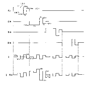
Figure 11 shows a set of drive signal
waveforms according to an embodiment of the present
invention.
At Sl - S4 are shown scanning selection
-27-
signals applied to mutually adjacent first to fourth
scanning lines Sl - S4 and at I is shown a succession
of data signals applied to a data line I in
synchronism with the scanning selection signals to
determine the display states of pixels on the data
line I. for example, a voltage at I-Sl is applied to
a pixel I-S2 at the intersection of the scanning line
S2 and the data line I.
A scanning selection signal includes a clear
pulse (A}, a first selection pulse (B) and a second
selection poise (C}. The clear pulse (A) is a pulse
for resetting the pixels on a scanning line to either
one of bright and dark states regardless of the
content of data signals synchronized therewith and has
a pulse width tl and a peak height VsQ.
The first selection pulse (writing pulse) (B)
is a pulse for inverting a 0 - 1Q0 °~ region of a reset
pixel in cooperation with a data pulse (Vil} applied
to a data line in syr_chronism therewith arid has a pulse
2Q width t~ and a peak height Vsl.
The second selection pulse (C) is a pulse for
causing at a pixel on a scanning line concerned (Si} a
display State corresponding to a data pulse (~i~)
determined based on a display state expected to be
displayed at a pixel on a subsequent scanning line
(S2}. It is to be noted that the pulse (C) is
different from a~known auxiliary signal.for canceling
212~.~2 7 4
the DC component on the scanning line. Such a known
auxiliary signal is set to have a pulse width and a
peak height determined so as not to change an already
formed display state of pixels concerned.
In contrast thereto, the second selection
pulse (C) in the present invention is set to have a
pulse width which are determined to change a display
state of a pixel on a scanning line concerned
depending on a display data for a pixel an a next
adjacent scanning line so as to compensate for a
possible threshold change at the pixel on the scanning
line concerned due to a temperature change, etc.
the second selection pulse (C) is applied in
succession to the first selection pulse (B) in
contrast with a pulse (C) shocrn in Figure ~ v~=hick is
applied after lapse of a certain period after a pulse
(B), in which period a pulse (B) for another scanning
line is also applied. In other words, a succession of
the clear pulse (A} and selection pulses ~B) and (C)
2fl are applied to an n-th scanning line and thereafter an
identical succession of the pulses (A), (B) and (C} is
applied to a subsequent (n+1)-th scanning line.
Accordingly, after the writing into pixels on
an n-th scanning line is completed inclusive of a
compensation for a threshold change, a subsequent
scanning line is selected, so that the subsequent
scanning line need ngt be a physically adjacent
-29- ~ ,~' 2 ~' e~%
(n+1)-th scanning line but can be an arbitrary
scanning line, such as an (n+10)th scanning line or an
(n+10~)th scanning line.
The scanning selection signal including the
pulses (A), (B} and (C} in Figure 11 may preferably be
adopted in an interlaced scanning scheme so as to
suppress a flicker on a panel which may be driven at a
low frequency according to the pixel shift method.
Alternatively, the scanning selection signal
may also be adopted in a partial rewrite scheme
wherein a part of scanning lines, e.g., m-th to
(m+1)th scanning lines, among all the scanning lines
are selected (repetitively) to partially rewrite a
part of the displayed picture, so as to effect a
~,5 mufti-window display at a high display quality free
from flicker.
In the above-mentioned pixel shift method,
before a pulse (C) for a pixel on an n-th scanning
line is applied, pulses (A) and (B) for a subsequently
2p selected scanning line are apglied, so that a
disturbance of a displayed picture is caused, if
skipping of scanning li,ne~ is performed as in an
interlaced scanning scheme or a random access as in a
partial rewrite.
25 The driving method according to the present
invention may be called a "random pixel shift method"
if the possibility of random access of scanning lines
2~2227r~
-3fl-
in the pixel shift method is noted.
Now, the driving method using the signal
waveforms shown in Figure 11 will be described in
further detail. When a succession of pulses shown in
Figure 12A (similar to a scanning selection signal
shown at S2 in Figure 11} is applied to a liquid
crystal layer at a pixel in an FhC device, the
orientation of the liquid crystal is reset to one
state (referred to as "DOWN"} by application of a
voltage pulse V~ (reset state}. Then, the liquid
crystal can be re-inverted from DOWN state to the
other orientation state (referred to as "UP"} by
application of a voltage pulse Vl. At this time, if a
pixel is grovided with a threshold distribution, e.g.,
by a cell thickness distrihution, it is possible to
effect a gradational display.
Nov.=, it is assumed that a pixel having no
threshold distribution is reset by application of
pulse V~y, then written ir_ UP by application of pulse
2Q Vl and further written in DOWN by application of pulse
V2. At this time, the magnitude of the voltage pulse
V2 required for uniformly orienting the pixel to DOWN
largely depends on the magnitude of the voltage pulse
V~ .
In a specific case wherein a liquid crystal
device cell identical to the one used in Examgle 1
described hereinafter was prepared and subjected to
212227
-31-
refresh-v,Triting by application of signals as shown in
Figure 12B (free from DC component as an average
voltage within one cycle} at a cycle of about 30 Hz
~t = 40 uses}. Figure 13 summarizes a relationship of
re-inversion voltage pulses V~ required for re-
inversion after application of tll pulses with varying
magnitude.
In Figure 13, the voltage V1 of the writing
pulse is taken on the abscissa, and the ordinate
lfl represents the peak height of the pulse V2 required
for re-inversion when applied subsequent to the pulse
V1 having a peak height indicated on the abscissa.
The results obtained at 30 oC and 40 oC are
respectively shown in Figure 13.
When the drive waveform shown in Figure 12B
is applied, the liquid crystal is reset to DOWN state
by application of the V~ pulse and then re-written to
UP state by application of the V1 pulse. According to
the data at 3~ oC in Figure 13, if the V1 pulse had a
2~ voltage value of 1.08 volts (pulse width = 4Q uses},
the orientation state could be re-inverted to DOWN
state by application of a V2 Pulse having a voltage
value of 2.fl volts. ~Iowever, if the V~ pulse had a
voltage of 11 volts, the Ll2 pulse required a voltage
Val'.le Of ~ VOl tS .
In this way, the voltage value required for
re-inversion by applicatior_ of the V2 pulse varied
-32-
depending on the tll pulse and was saturated above a
certain V1 pulse as shown in figure 13. In either
case of V1 - 10.0$ volts or 12 volts, the pixel was
entirely written in UP when the V2 pulse was 0 volt.
Accordingly, it is also understood that, even if two
pulses equally forming UP state are applied and then a
re-inversion pulse for writing DOWN is applied, the
magnitude of the re-inversion pulse required for the
reinversion varies depending on the magnitude of the
preceding pulse for forming UP state. The UP states
formed by application of two tll pulses having
different magnitudes appear to be optically identical
to each other but can have different molecular
alignment states. In other words, it may be said that
the threshold for re-inversion by the V2 pulse varies
depending on the state of liquid crystal molecules
subjected to application of the V2 pulse.
The phenomenon that the re-inversion
threshold voltage by application of the V2 pulse
2p varies depending on the magnitude of the preceding tll
pulse and is saturated above a certain V1 voltage, is
equally obsercred at different temperatures (Figure
13}.
Further examination of the relationship
betcNeen testy pul se and the V2 pulse has al so shown
the folloir:ing fact.
If voltages V1 and V2 are normalized so as to
f
212224
-33-
provide "1" at the saturation of the re-inversion
voltage t12, a relationship shown in Figure 14 is
obtained. Figure 14 shows that the above-mentioned
characteristic shows little dependence on temperature.
That is, with reference to the V1 and V2 values at the
saturation of the re-inversion voltage V2 versus V1,
if V1 causes a certain proportion of change, V2 also
causes a corresponding proportional change. More
specifically, if V1 reduces to 0.$ with respect to a
reference value (i.e., Vl at the saturation of V2), V2
uniformly reduces to about 0.2 with respect to a
reference value (i.e., tl2 at the saturation of tl2 ar
maximum V2) regardless of the temperature being at 30
aC or 40 aC.
Fram the characteristics shaven in Figures 13
and 14, in the case where a driving voltage wavefarm
as shown in Figure 12A or Figure 12B is applied to a
liquid crystal layer in an FLC device having a
threshold distribution in a pixel, it is possible to
estimate the quantity of re-inversion by application
of a V~ pulse after writing by application of V1
pulse. According to Figure 14 showing results
obtained by a decTice having a cell thickness gradient
in a pixel, it is understood that, when a pixel is
written to a cell thickness dl and then supplied with
pulses of V3 = 1 (normalized value) and V2 = 0.6, the
domain walls can be reinvented in the range of 1 - 0.$5
_34_
up to a cell thickness position of dl; d2 = 0.$5.
The phenomenon is further described with
reference to Figure 15. At a low temperature T1, a
pixel is written in W1 ~ by application of a V1 pulse
and returned by WW1 °~ by application of a tl2 pulse.
At a high temperature T2, a pixel is written in W2 ~
(W2 > W1) by application of the tll pulse and returned
by SW2 ~ by application of the VZ pulse. At this
time, WW1 =bW2. This means that the change in written
amount (8W1 and bW2) by a succession of the V1 and V2
pulses is constant regardless of the temperature.
Accordingly, a data quantity ~Q obtained by removing a
writing change 6W2'caused by a temperature change does
not depend on the temperature. Accordingly, if a
writing quantity change (&W2' in the above) can be
corrected separately, a gradation data can be written
by a succession of pulses Vl and V2.
Figure 16 illustrates functions of the V1 and
tT2 pl~lses. Referring to Figure ?~, both a high
24 temperature pixel and a low temperature pixel are
reset to a v.=holly black state by application of a VQ
pulse and then written into "white" by application of
a Vl pulse. The white-writing quantity by the V1
pulse differs at a high temperature and a low
temperature, and the difference is corrected by a V2
pulses. More specifically, by application. of the V~
pulse subsequent to the Vl pulse, (a} the written
2~2~2'~~
-35-
state formed by the Vl pulse is corrected, and (b} the
temperature-dependent different or deviation is
corrected. The voltage value for the V2 pulse is
determined first for fib} the temperature-dependent
deviation, and then the Vl voltage is determined so as
to obtain a desired written quantity when followed by
the V2 voltage guise.
According to Figure 14, it is possible to
know a re-inversion quantity by application of the
l~ determined V2 voltage pulse depending on the magnitude
of the Vl voltage pulse, so that a desired gradation
can be written by determining the V1 voltage while
taking the re-inversion quantity into consideration.
The above driving principle is applicable not
only to a device having a cell thickness gradient
(electric field intensity distribution} in a pixel a
shown in Figure 6 but generally to a device having an
inversion threshold distribution in a pixel.
In the above, it has been described possible
2~ to display a certain data by removing a succession of
Vl and V? gul ses kTh~l a rer.~oving the temperature-
dependent deviation. Now, a temperature-compensation
function of a V~ Pulse will be described with
reference to Fig~,~ra 1 ? .
In Figure 1?, the abscissa represents a
transmittance I~ ~~}. A device is assumed to have a
monotonous threshold distribution in a pixel as shown
21222' ~~
-36-
in Figure 6 so as to satisfy a linear relationship
between the transmittance W and the logarithm of a
voltage (ln ~l} at constant pulse width. It is
actually possible to design such a cell thickness
gradient.
In case of writing in a pixel on a scanning
line (N) which is assumed to be subjected to a
sequence of "black" reset and "whit" writing, a
correction pulse Zl2 is set in a direction of writing
I~ "black". Correspondingly, a subsequently selected
(N+1}-th line may be subjected to a sequence of white
reset, black writing and white correction. This is
because the data on the tN+1)th line is shifted toward
the N-th line corresponding to a temperature
deviation, the data carried by V2 is naturally in the
black writing direction in order to enter the N-th
line and the expected gradational display on the (N-
th}-th line by X11 is in the direction of writing
bl ack .
In the present invention, a temperature range
T~ _ T2 allo~:ing a temperature comgensatior_ is such a
temperature range that the threshold change of FLC due
to the temperature change amounts to l;x whereir_ x
denotes a threshold ratio in a pixel. This means a
temperature range such that the locaer limit of the
threshold distribution at Tl is equal to the upper
limit of the threshold distribution at T2. V~ assumes
21222'4
-37-
a voltage range of Lj21 - Z'22 allowing gradational
display of 0 - 100 ~ corresponding to the threshold at
T2 (before being affected by Vl).
In Figure 17, a horizontal line i represents
a threshold of inversion after resetting at a low
temperature T1. Accordingly, if a voltage in excess
of i is applied, FLC causes a state inversion thereof.
Herein, the V1 pulse and the V2 pulse have symmetrical
thresholds while their polarities are different and,
1Q in Figure 17, the voltages are indicated with an
identical sign.
Next, the setting of V2 and V1 based on
expected gradation data will be described. In
consideration of the inversion threshold change due to
V1 described with reference to Figures 13 and 14, V11
is assumed to represent a value of VI by ~.~hich the
resultant state is returned to 0 ~ display by
application of V21, and V12 is assumed represent a
value of VI capable of retaining 100 s display even
after application of V~2, so that V1 can assume a
voltage range of V11 - V1~. Solid lines a - d in
Figure 17 represent V12, V11, V22 and V2I,
respectively, and actually have slopes because of an
electric field intensity gradient due to a threshold
distribution in a pixel.
Referring to Figure 17, vthpn V~1 is applied,
a pixel is caused to have a gradation of Q1 (~) at
-38-
which a domain wall (hereinafter called a "wave plane
Q1") is formed. By the application of V11, the
inversion threshold is changed from i to a dashed line
e. The inversion threshold change ratio is constant
as described before. With respect to the wave plane
Q1, any voltage of V21 - V22 exceeds the above-
mentioned e, so that the pixel is returned to 0 %
display by the application of V2. Further, in case
where Vq slightly higher than V11 is applied as V1, a
lp pixel is caused to display a gradation of Q2 (%)
higher than Q1 and the inversion threshold is changed
to a dashed line f. With respect to the line f, V22
is always not below the line so that the wave glane
Q1 is inverted to 0 % display by application of V22
but V21 is partly below f, so that the inversion
cannot be effected at the part. The part is denoted
by Q3 in Figure l~. Accordingly, in case where a
gradation of 0 % is expected to be displayed, V11 may
be apglied as Vl even if V2 determined based on
2fl gradation data is any of ~T21 - V22- In case where a
gradation of Q3 is exgected to be displayed, Vq may be
applied as V1 for V21, and a voltage higher than Vq
may be applied for V22 since 0 % display results if V1
- Vq. For displaying a gradation of 100 %, a value of
V1 providing Q4 is applied for V2 = ~~21 and a value of
V1 providing Q5 is applied for ZT22- More
specifically, V.1 providing Q5 is V12-
y,
39
Incidentally, the gradation display upper limit
is 100 %, Q4 and Q5 actually mean 100 o display
but, as the inversion threshold change depending
on Vl is present, Q4 and Q5 are indicated in
excess of 100 o so as to cover such cases. Dashed
lines g and h represent the respective threshold
changes.
A temperature change in Figure 17 is assumed
to correspond to an increase in applied voltage V1 and
V2 relative to the inversion threshold of the liquid
crystal and is regarded as identical to parallel
movement of 0 ~ position and 100 ~ position toward a
K-axis. This corresponds to parallel movement of a
[0, 100] region to a [-100, 0~ region in Figure 17.
In case of a temperature increase, writing by
a V2 pulse occurs in a 0 ~ side. This is because VZ
for an N-th line is determined by gradation data for
an (N+1)-th line. Thus, the threshold is lowered due
to the temperature increase and, corresponding to the
threshold change, the gradation data for the (N+1)-th
line is written on the N-th line. On the N-th line;
V2 and V1 are of mutually opposite polarities. The
writing directions on the N-th and (N+1)-th lines are
mutually opposite. Accordingly, the shift of
gradation data for the (N+1)-th line by V2 is effected
in black-ceriting if the N-th line is subjected to
white writing. Gradation data for the N-th line is
A
212224
-40-
shifted to an (N-1)-th line by tl2 corresponding to the
shift of gradation data for the (N+1}-th line thereto.
Accordingly, gradation data are displayed while being
sequentially shifted to adjacent lines. For example,
in case where the gradation data for the (N+1)-th line
is 50 %, a pixel is inverted to 50 % black by black
writing with V1 at T1 and, even if 50 % of gradation
data is shifted to the N-th iine due to a temperature
increase, the gradation data shifted to the N-th line
is the remaining white (50 %), so that no black
~=citing by ~l2 is caused on the N-th line. In the case
of the same 50 % shift, however, if the gradation data
on the (N+1}-th line is 80 % black, the remaining 20 %
white and 30 % black are shifted to the N-th line, so
that 30 % black writing is effected by ~I2. If the
gradation on the (N+1}-th line is 100 % black, 50
black writing is effected by ~2 on the N-th line.
The above point will be further described
with reference to Figure 17, wherein an intersection
of a dot-and-dash line I and a solid line i provided a
projection Q~ on the abscissa which is at an exactly
mid point in the range [-100, 0], so that the line i
exceeds the incrersion threshold in the range ~-100,
Q5) and is below the inversion threshold in the range
[QS, 0]. Accordingly, in case of the V~ pulse having
a voltage of ~2j, writing on the 0 % side does not
occur unless the threshold change due to a temperature
..a 212227
-41-
change requires a rewriting of 5C~ ~ or higher.
A necessary condition for effectW g a drive
in combination with temperature compensation by
applying a succession of V1 and V2 pulses according to
the present invention is that the liquid crystal
threshold distribution after writing with the V1 pulse
is steeper than the electric field intensity
distribution applied to the pixel.
According to the above-described driving
principle, as shown in strips at the lower part of
Figure 17, data (indicated as a hatched part}
displayed on scanning lines are continuously changed
from a low temperature ~T1} to a high temperature (TZ}
so that data expected to be displayed on an ;N~?}-th
line at T1 is displayed on an N-th line at T2.
According to the driving method of the
present invention, when an entire liquid crystal panel
is at a temperature of, e.g., T1, all the pixels
effect expected gradational display of their own
2Q scanning liens and, when the entire liquid crystal
panel is at a temperatl.:re T~, all the pixels display
gradation data or. respectively subsequent scanning
lines. Accordingly, in the latter case, the display
is deviated by one line but the one-line deviation can
be substantially ignored since an actual liquid
crystal panel includes a large number of scanning
lines. Further, in case where a temperature gradient
21~227~~
-42-
from a side of Tl to an opposite side of T1 is
developed along a panel, the expected display is
performed on the T1 side but the shift of gradation
data is gradually increased toward the T2 side. As
described above, however, one-line shift can be
substantially negligible and adjacent two scanning
lines can be regarded as at the same temperature, so
that substantially no problem is caused by such a
temperature distribution.
Figure 18 is a block diagram of a liquid
crystal apparatus including a drive circuit for
supplying a drive signal waveform as shown in Figure
11 to a liquid crystal panel 32. Referring to Figure
18, the apparatus includes an image data source 21 for
supplying a set of image data I1 for pixels on a
scanning line and image data I2 for pixels or. a
subsequently selected scanning line. These data are
converted into binary signals by an A/D converter 22.
The binary signals are divided through a controller 23
to scanning signals and data signals supplied to a
scanning side drive circuit and a data side drive
circuit. The data side drive circuit includes a data
signal generator circuit 24 for determining Vj2 {V2
for pixels on a j-th scanning line) from the image
data I2 and a data signal generator circuit for
determining Vjl (V1 for pixels on the j-th scanning
line) from Vj2 and Il. These data signals are
2122274
-43-
supplied through a data side shift register 26, a
decoder 27 and an analog switch 28 to the liquid
crystal panel 32.
The scanning side drive circuit includes a
scanning side shift register 29, a decoder 30 and an
analog switch 31, through which scanning selection
signal are supplied to scanning lines constituting the
liquid crystal panel 32 based on scanning line address
data.
Another suitable embodiment of the liquid
crystal apparatus according to the present invention
may include a liquid crystal device having a structure
as shown in Figure 5 including a film 54 betv.=een the
electrode and the liquid crystal layer, which film is
characterized by a volume resistivity of at most 108
ohm. cm and drive means suitable for causing partial
inversion in a pixel. The driving may preferably be
performed by the pixel shift method, the four pulse
method and the random pixel shift method described
2 fl above .
The film disposed between the electrode and
the liquid crystal layer used in the liquid crystal
apparatus of the present invention is characterized by
having a volume resistivity of at most 108 ohm.cm,
preferably 104 - 107 ohm. cm. In case where the film
has a volume resistivity of belov~: 104 ohm.cm, an
electrical continuity between the pixels cannot be
..e 21222'~~~
-44-
ignored, so that it becomes necessary to pattern the
film similarly as the electrode. It is desired that
the film has a thickness of at most 2QOQ ~, preferably
at most 100 14.
The film may preferably comprise a known
alignment film material, such as polyimide or
polysiloxane, containing conductive or semiconductive
fine particles, such as those of Sn0? and In203,
thereir_. Alternatively, the film may have a laminar
structure comprising at least two layers including an
alignment film of an organic conductor, such as
polypyrrole, polyaniline or polyacetylene, or a known
organic insulating alignment film material, such as
polyimide, on the liquid crystal side; and an
~5 inorganic film layer of a conductive or semiconductor
material such as SnxOy, InxOy or a composite of these,
or an inorganic insulating material on the electrode
side.
The film may have an appropriate composition,
?~ dopant content or thickness ratio so as to provide a
volumetric resistivity of at most 10~ ohm. cm,
preferably 1~4 - 1C~~ ohm. cm. The volumetric
resistivity VR of a laminate film may be calculated as
fol losots:
25 VR = (VRl tl + VR2~t~ + ...)/(tl -~ t? ...),
~rherein VR1, R~ ... denote the volumetric
resistivities of the materials constituting the
2122274
-45-
component layers and tl, t2 ... denote the thicknesses
of the component layers.
The liquid crystal device having such a film
between the electrode and the liquid crystal layer,
preferably on both substrates, may be included as a
display panel 103 in an liquid crystal apparatus as
represented by a block diagram shown in Figure 19.
More specifically, Figure 19 is a block
diagram of a control system for a liquid crystal
1~ display apparatus as an embodiment of the liquid
crystal apparatus according to the present invention,
and Figure 20 is a time chart for communication of
image data therefor. Hereinbelow, the operation of
the agparatt~s will be described ~:ith reference to
these figures.
A graphic controller 102 supplies scanning
line address data for designating a scanning electrode
and image data PD0 - PD3 for pixels on the scanning
line designated by the address data to a display drive
2~ circuit constituted by a scanning line drive circuit
104 and a data line drive circuit 105 of a liquid
crystal display apparatus 101. In this embodiment,
scanning line address data ;A0 - A15) and display data
(D0 - D1279) must be differentiated. A signal AH/DL
is used for the differentiation. The AH/DL signal at
a high (Hi) level represents scanning line address
data, and the AH/DL signal at a loc.= ;Lo) level
2122274
-4s-
represents display data.
The scanning line address data is extracted
from the image data PDO - PD3 in a drive control
circuit 111 in the liquid crystal display apparatus
101 outputted to the scanning line drive circuit 104
in synchronism with the timing of driving a designated
scanning line. The scanning line address data is
inputted to a decoder 106 within the scanning line
drive circuit 104, and a designated scanning electrode
1Q within a display panel is driven by a scanning signal
generation circuit 107 via the decoder 106. On the
other hand, display data is introduced to a shift
register 108 within the data line drive circuit 105
and shifted by four pixels as a unit based on a
transfer clock pulse. then the shifting for 1280
pixels on a horizontal one scanning line is completed
by the shift register 108, display data for the 1280
pixels are transferred to a line memory 109 disposed
in parallel, memorized therein for a period of one
horizontal scanning period and outputted to the
respective data electrodes from a data signal
generation circuit 110.
Further, in this embodiment, the drive of the
display panel 103 in the liquid crystal display
apparatus 101 and the generation of the scanning line
address data and display data in the graphic
controller 102 are performed in a non-synchronous
_4~_
manner, so that it is necessary to synchronize the
graphic controller 102 and the display apparatus 101
at the time of image data transfer. The
synchronization is performed by a signal SYNC which is
generated for each one horizontal scanning period by
the drive control circuit 111 within the liquid
crystal display apparatus 101. The graphic controller
102 always watches the SYNC signal, so that image data
is transferred when the SYNC signal is at a low level
1Q and image data transfer is not performed after
transfer of image data for one scanning line at a high
level. More specifically, referring to Figure 19,
when a low level of the SYNC signal is detected by the
graphic controller i02, the AH/DL signal is
immediately turned to a high level to start the
transfer of image data for one horizontal scanning
line. Then, the SYNC signal is turned to a high level
by the drive control circuit 111 in the liquid crystal
display apparatus 101. After'comgletion of writing in
the display panel 103 with lapse of one horizontal
scanning period, the drive control circuit 111 again
returns the SYNC signal to a low level so as to
receive image data for a subsequent scanning line.
Example 1
As a first embodiment, a liquid crystal cell
having a sectional structure as shown in Figure 5 caas
prepared. The lower glass substrate 53bwas provided
-4$_
with a saw-teeth shape cross section by transferring
an original pattern formed on a mold onto a UV-curable
resin layer applied thereon to form a cured acrylic
resin layer 52.
The thus-formed UV-cured uneven resin layer
52 was then grovided with stripe electrodes 51b of ITO
film by sputtering and then coated with an about_300
~-thick alignment film 54b(formed with "LQ-1802",
available from Hitachi Kasei K.K.).
lp , The upper glass substrate 53a was provided
with stripe electrodes 51a of ITO film on a flat inner
surface and coated with an alignment film 54a, identical
to alignment film 54b.
Both substrates 53a, 53b (more accurately, the
alignment films 54a, 54b thereon) were rubbed respectively
in one direction and superposed with each other so
that their rubbing directions were roughly parallel
but the rubbing direction of the lower substrate
formed a clockwise angle of about 6 degrees with
respect to the rubbing direction of the upper
substrate. The cell thickness (spacing) was
controlled to be from about 1.10 dun as the smallest
thickness to about 1.64 pm as the largest thickness.
Further, the lower stripe electrodes 51 were formed
along the ridge or rigple (extending in the thickness
direction of the drawing) so as to provide one pixel
width having one saw tooth span. Thus, rectangular
a
2122274
-49_
gixels each having a size of 300 gm x 20y.~.m were
formed.
Then, the cell was filled with a chiral
smectic liquid crystal showing the following phase
transition series and properties.
Table 1 (liquid crystal)
$2.3 oC 76.6 oC 54.$ oC
I so . t ~ Ch c ~ SmA'~ ~' SmC'~
$1.$ oC 77.3 oC
1~ -2.5 oC -20.9 oC
Cryst
Ps = -5.$ nC/cm~ (30 oC)
Tilt angle = 14.3 deg. (30 oC)
~E - _0 X30 oC)
I5
The liquid crystal cell (device) thus
grepared was driven by applying a set of drive signals
shown in Figure 11. The respective pulses were
characterized by parameters of tl = 150 uses, t2 = 40
2Q uses, Vs~ _ ?.0 volts, Vsl = 13.1 volts, Vs2 = 6.9
Erol ts, -3. 1 volts ~ Vi 1 5 3. 1 volts, -1 . 41 t=cl is s Vi2
1 . 41 STol tS .
The liquid crystal device driven in the
above-described manner shes-red a display characteristic
25 represented by a curve P~ in Figure 21 wherein the
abscissa represents Vl - nst - Vil and the ordinate
represents a relative transmittance (3).
21222' 4
On the other hand, when the same device was
driven in the same manner by using driving waveforms
shown in Figure 11 while omitting the pulses
corresponding to the selection signal (c) (i.e., Vs2 =
0 and Vi2 = 0), the device showed the display
characteristics represented by curves B in Figure 21.
Thus, in this case, the resultant transmittances were
remarkably different depending on a temperature
change, thus failing to show a good gradation
characteristic.
In contrast thereto, the curve A obtained
according to the drive method of the present
invention showed a good gradation characteristic with
temperature compensation. Incidentally, a better
gradation display characteristic with less influence
by a subsequent data signal was obtained when a longer
interval period (Y in Figure 11) was placed between
successively applied data signals, and a particularly
good result was attained when Y was about 200 usec.
FxamF~l a 2
A liquid crystal cell (device) having a cell
thickness gradient as showr_ in Figure 22 was obtained
in a similar manner as in Example 1 except that the
cell thickness distribution was in the range of 1.0 -
1.4 um, and the rubbing directions applied to the two
substrates were set to cross at an angle of about 10
degrees in addition to the change in the sectional
2122274
-51-
structure. The device was driven by applying a set of
drive signals as shown in Figure 11 by using a circuit
as shown in Figure 18.
The liquid crystal device used in this
Example included pixels formed by scanning lines 54
each having a width A as shown in Figure 22, so that
it could not cause a complete pixel shift as described
hereinabove. However, as the brightness control could
be effected in the device, a temperature compensation
could be effected according to the driving method of
the present invention. Figure 23 schematically show a
display state formed in this Example.
In each of the above-descrihed Examples 1 and
2, the gradational display drive was effected by
voltage modulation, but the modulation can also
effected by either pulse width modulation or phase
modulation.
Example 3
In Example l, the best result was obtained
when. the length of Y eras set to about 20~ psec. In
this Example, it was tried to shorten the period Y by
applying a crosstalk prevention signal determined
based on a data signal. The other features were
identical to those adopted in Example 1.
In order to produce a crosstalk prevention
signal, the effect of pulses applied immediately after
the Vs2 pulse in the waveform shown in Figure 11 is
21222'~~
-52-
examined with tide. Figure 24 summarizes the
analysis.
Figure 24(a} shows a waveform except for the
period Y. At (b} are shown addresses of the waveform.
At (c) are shown experimentally measured effect
factors obtained when the waveform at (a} was applied
subsequent to the Vs2 pulse. At (d) are shown example
voltages of pulses included in the waveform at (a).
These values are determined based on image data for a
pixel on a scanning line concerned and image data for
an adjacent pixel on an adjacent scanning line
similarly as in Example 1. At (e) are shown values
obtained by dividing the values at (d) with the values
at (c). If the applied voltages at the period Y are
~5 assured to be VYl and VY2, the effects thereof are
shown as VY1; 3 and ZlY2% 7~ respectively.
The total of the values at (e) from Address 3
to Address ?~ amounts to ~.Q~7. This value may be
reduced to zero by adjusting the voltages within the
Period Y. The values of VY1 and VY2 therefor must
satisfy the following conditions:
(VY1~3) t (VY2~~) - -0.0037
VYl - -VY2
By solving the above equations, VY~ and VY2
are obtained as follows:
VYl - -0.2 volt
VY2 = 0.2 volt
53
By determining the waveform within the period
Y in the above-described manner, it is possible to
accomplish a good gradational display with less
crosstalk.
Example 4
A liquid crystal cell (device) having a
sectional structure also as shown in figure 6 was
prepared in the following manner. The lower glass
substrate 5~ was provided with a saw-teeth shape cross
section by transferring an original pattern formed on
a mold onto a UV-curable resin layer applied thereon
to form a cured acrylic resin layer 52.
The thus-formed Utl-cured uneven resin layer
52 was then provided with stripe electrodes 51b of ITO
film by sputtering and then coated with a film 54b,
which was formed by applying a solution of polyaniline
(molecular weight = ca. 200 - 300) and camphor-
sulfonic acid (as a strong acid) at concentrations of
0.7 wt. ~ and 0.3 wt. ~S, respectively in a mixture
solvent of N-methylpyrrolidone and n-butylcellosolve
by spinner coating at 1500 rpm for 20 sec, followed by
baking at 20~ oC for 1 hour.
The upper glass substrate 53a was provided
v:ith Stripe electrodes 51a of ITO on a flat inner
surface and coated with an identical polyaniline film
54ain the same manner as above.
As a result of separate formation of an
~~. ~ ~ Fy.
-54-
identical film 54a under the same conditions as above
on a flat ITO coated glass substrate, the film 54a
showed a thickness of ca. 4O0 ~ and a volume
resistivity of ca. 1~~ ohm. cm.
The two-substrates were subjected to rubbing
in the same manner as in Example 1. Further, by using
the above-treated two substrates and the same liquid
crystal material as in Examgle l, a liquid crystal
device including pixels each having a size of 300 ~.un x
1Q 200 ~.un was pregared otherwise in the same manner as in
Example 1.
Figure 25 is a waveform diagram showing a set
of driven signal waveforms used in this Example
including scanning signals applied to scanning lines
sl, s?, ~3, ..., data signals applied to a data line
I, and a combined voltage signal applied to a pixel S2
- I (i.e., a gixel at the intersection of the scanning
line, and the data line I}.
In this Example, a gradation drive scheme
according to the pixel shift method was adopted, so
that adjacent to=o scanning lines were supplied with
scanning signals having mutually reverse polarities at
corresponding Phases.
Referring to Figure 25, the respective pulses
were characterized by parameters of E~le~, _ 18.0 volts,
~vs~ - 17.0 volts, ft~ij - 5.0 volts, T = 4o uses, ~ _
2~ usec, tl = 7 psec and t2 = 7 psec.
a
2122274
-55-
The data signal modulation was effected
according to a phase modulation scheme, and an outline
of the data signal modulation is illustrated in Figure
26B. Figure 26B shows data signal voltage waveforms
in the range of I~(Q ~) to I (1Q0 °s) for displaying
the states respectively indicated in the parentheses.
In the respective data signals, the width of a pulse
portion A is variably modulated so as to provide a
voltage signal having a width ~ with writing data.
The modulation of the portion A is set so that the
width ~ and the marginal width of the 4T have a ratio
of 1/r : ( 1-1; ~') .
Such a ratio is set so as to make continuous
the thresholds of inversion at a pixel which has been
supplied with a scanning signal A in the first writing
and a scanning signal B in the second writing in
Figure 25. The width 8 is 1/~' of the selection period
QT of the scanning signal A. This condition is also
given in order to make the thresholds continuous.
2~ Herein, ~' denotes a slope aT;a71 on a curve shown on a
coordinate system having an ordinate of transmittance
(T) and an abscissa of modulation parameter (~) as
shown in Figure 1SA.
Now, the modulation parameter (a) will be
described. Figure 2? sho~s~s a gragh shov.Tir_g a
relationship between transmittance (T) and modulation
parameter (~). In the case of using a modulation
-5~-
X
scheme as shown in Figure 26B ~ the abscissa is
expressed on a logarithmic scale (ln) so as to
represent the change in threshold of a liquid crystal
by a parallel shift on the graph. In the drive scheme
shown in Figure 25, the voltage applied to a pixel
corresponding to a scanning selection pulse A in a
scanning signal varies in a range of from a
rectangular voltage of VI - Vth = 14 volts (as shown
at (b-I) of Figure 27B) to a rectangular voltage of V3
IO - Vsat = 20 volts (at (b-3) of Figure 27B}.
Then, if a modulation parameter (T) is
defined as a period (pulse width} weighed (e. g.,
multiplied) by a (varying) voltage, it is possible to
obtain a relationship between transmittance (T) - 1nT
which is linear and may be shifted in parallel in
accordance with a temperature change.
The manner of weighing with a voltage (peak
value) is explained based on an example. A pulse
having a portion showing a peak value V1 in a pulse
length of tl (in total if two portions having Vl are
present} and a portion having a peak value V2 in a
pulse length t2 may be determined to have a modulation
parameter given by:
T = (V2/V1}~tl+t2.
In case of Figure 27B, tI + t2 - 40 usec, V1 - 14
volts and V2 = 20 volts.
If T is determined in this way under the
0
conditions of Figures 25 and 26, the selection voltage
waveform varies in the range of from an L-shaped one
having a portion of 10 volts - 32 usec and a portion
of 22 volts - $~asec to a rectangular one having a 100
~-portion of 22 volts - 40 usec.
The above range is used for gradational '
display and a pulse of 10 volts - 40 psec is used for
display of 0 ~. The latter corresponds to a voltage
waveform given by a data signal I (-0 ~) in Figure
26B.
By disposing a low-resistivity film layer
between the liquid crystal and the electrode as
described above, it was possible to increase the
stability of domain walls in a pixel during plural
times of writing for a pixel, and also possible to
provide an increased degree of additivity in
temperature compensation.
Further, the irregular movement of domain
wall and fusion or connection of domain walls as
described with reference to Figure 10(c) and (d) were
prevented until the spacing between domain walls was
reduced to 10 - 20 lun, compared with 20 - 30 um as in
a conventional device. Further, the number of
reliably displayed gradation levels could be increased
from about $ to about 13, thus providing a remarkably
improved gradational display characteristic.
Example 5
a.
T 21222' 4
-58-
A liquid crystal cell having a sectional
pixel structure as schematically shown in Figure 28
was prepared. The cell included an uneven substrate
structure including a glass substrate 41a, an uneven
ITO film 32a, an Sn02 layer 43a and a polyaniline
layer 44a; an even substrate structure including a
glass substrate 41a, an ITO film 42b, an Sn02 layer
43b and a poiyaniline layer 44b; and an FLC layer 45
disposed between the substrates.
The ITQ film 42a was provided with ca. 2 um-
wide stripe projections extending in the direction of
thickness of the drawing which were spaced thee
different pitches of 2 pn, 3 ~.un and 5 pm laterally
from one side to the other side.
I5 The Sn02 films 43a and 43b were formed in a
thickness of 900 A by ion plating at a rate of 6 A/sec
in an Ar;Q2 ~i00/70; mixture environment under the
conditions, the resultant Sn02 film showed a volume
resistivity of ca. 105 ohm.cm. Such an Sn02 film may
2~ also be formed by sputtering in a volume resistivity
of, e.g., i0f - 10~ ohm. cm.
The thus formed SnO~ film 43a and 43b were
coated with poiyaniline layers 44a and 44b,
p pe 7e y n a hi ~ na gf ~Y 1 nn a aa~j~ in the
r~s ctii i , i__ t___~k_.~ss . ,
?5 same manner as in Example 4. The resultant laminate
film including the SnQ2 film and the polyaniline film
showed a voiump resistivity of 1.5x10 ohm. cm.
21222' 4
=59-
The resultant polyaniline layer 44a on the
uneven substrate was provided with stripe projections
of ca. 2000 ~. in height corresponding to the uneven
ITO film 42a and rubbed in a direction of the stripe
projections. The golyaniline layer 44b on the other
even substrate was also rubbed in one direction. The
two substrates were applied to each other with Si02
spacer beads (of 1.4 ~.un-dia.} dispersed therebetween
so that the rubbing direction on the even substrate
formed a clockwise angle of 10 degrees with respect to
the rubbing direction of the uneven substrate as
viewed from the uneven substrate.
The resultant blank cell was filled with the
same liquid crystal material as in Example 1 to form a
liquid crystal cell.
The thus-formed liquid crystal cell was found
to show a gradational display characteristic such that
domain inversion was initiated from a side of pitches
being formed with a smal l spacing ( 2 ~.~.m } and
propagated toward the other side in a pixel. At a
pulse width 4T = 40 gsec, the inversion was partly
initiated at V = i8 volts and 100 % inversion was
caused at 22 volts, th~.a sho~:ing a threshold
distribution rate of 1.22.
By forming ar_ electroconductive primary layer
(Sn02 layer) below the alignment layer as described
above, the domain stability was improved. When the
2i2~~~i
-60-
device was subjected to a matrix drive by application
of waveforms shown in Figure 25, disappearance of
small domains (2 pm or smaller in diameter) was
suppressed and the stability of domains were increased
against plural times of writing in a pixel, thus
providing an improved display characteristic.
As described hereinabove, a gradational
display system capable of correcting a temperature-
dependent deviation and also capable of interlaced
scanning drive is provided by applying specific
sequential pulses after a clearing pulse. As a
result, it has become possible to realize a good
gradational display with reduced flicker and contrast
irregularity.
Further, in a liquid crystal apparatus
according tc the present invention using a liquid
crystal device wherein a low-resistivity film layer is
disposed between the liquid crystal layer and the
electrode, the stability of liquid crystal molecules
2fl in the vicinity of domain walls formed by partial
inversion in a pixel is improved, thereby realizing a
mere accurate and stable gradational display while
performing temperature compensation.