Note: Descriptions are shown in the official language in which they were submitted.
wo 93/21706 2 ~ 2 3 2 2 0 pcr/GBg3/oo747
OP~T t~ ~T. ~Rr~F.C .CT IPt: .C ~
$his invention relates to an optical processing
system, and in particular to optical header recognition in
packet switching networks.
; In a circuit switched telecommunications networ~, a
physical circuit is made between two terminals for the
duration of a call. For certain traffic formats, such as
speech, the information being transmitted never completely
fills the connection between two terminals, that-is to say
10 the start of the information does not reach the destination
terminal before the end of that information leaves the
transmitting terminai, but the circuit is held open for the
duration of Ihe infor~ation~s transmission between the two
terminals. With high-speed circuits carrying digital data,
15 a much greater resource utilisation is possible by sharing
paths through the network. A packet switching network is one
way of achieving this improved resource utilisation, data
being transferred through the network in packets. Each
packet includes, apart from the data itself, a header
20 containing addressing and seauence (control) information for
controlling the progress of that packet through the network.
The addressing and seauence information coded in the header
of a packet is.decoded at the network nodes to provide
routing control. A packet switching network tbus provides a
25 virtual circuit between two terminals, this circuit appearing
to the u ers as a permanent connection between the terminale
but which, in fact, is shared with other u ers.
Rnown methods of coaing packet he~ers rely on time
correlation techniques. The utilisation of a packet
30 switching network is linked to the bit-rate. The utilisation
also depends upon the ratio of data time to wasted time, that
is to say the ratio of the time the network is transmitting
data to the time data is not being transmitted. In the time
domain, the wasted time is made up of the time taken up with
35 he~er transmission (the heA~er of a packet occupying a
separate time slot at the head of the data of that packet),
WO~3/217~ PCT/GB93/00747
2123220 - 2 -
. and by the guard band transmission time, the guard band being
the separation between adjacent packets which is e~sential to
avoid overlap of the packets due to dispersion during
transmission.
The aim of the invention is to provide an alternative
techniaue for coding and decoding header inf ormation,
particularly in packet switching networks, which technique
results in increased network utilisation.
The present invention provides a telecommunications
system comprising first and second nodes interconnected by a
network transmission line, the first node comprising an
optical data generator for producing an optical data signal
at a first wavelength, an optical header generator for
producing an optical control (header) signal at a second
15 wavelength, means for multiplexing the data and control
signals onto the transmission line in such a manner that the
duration of the control signal is at least equal to the
duration of the data signal, a delay unit and control means
associated with the delay unit for providing a sufficient
20 delay between the transmission start times of the control and
data signals to ensure that the control signal completely
overlaps the data signal on arrival at the second node, the
second node comprising a switch and a controller responsive
to signals at the second wavelength for controlling the
routing of optical signals through the switch.
As the control signal overlaps the data signal, the
two signals occupy the same time slot.
Advantageously, the optical data generator produces
optical data signals in packets, and preferably the optical
30 data generator is constituted by a laser and a modulator for
modulating the output of the laser. The header generator may
also be constituted by a laser.
The system may further comprise a modulator for
modulating the header laser so as to turn the header laser on
at, or just before, the start of a data packet and to turn
the he~er laser off at, or just after, the end of a data
packet.
W093/21706 212 3 2 2 0 PCT/GB93/00747
-- 3
Convenlently, the controller of the second node
includes a splitter for demultiplexing a portion of the
control signal, and a narrow band-pass filter whose pass band
is centred on the second wavelength, the output of the filter
S being used to control the operation of the switch. An
amplifier may be positioned between the splitter and the
filter.
Advantageously, the switch is an optical switch such
as a NLOA. Alternatively, the switch is an opto-electronic
10 switch. In either case, the switch may have two outputs, one
of which leads to a further network transmission-line, and
the other of which leads to a receiver. Preferably, a narrow
band-pass filter is positioned between the switch and the
receiver, the pass band of said filter belng centred on the
first wavelength.
Prefera~ly, there is a plurality of second nodes, the
nodes being interconnected ~y network transmission lines, and
the optical data generator and the optical header generator
of the first node are tunable so as to provide data and
control signals at predetermined, different wavelengths for
each of the second nodes.
In a preferred embodiment, the or each second node is
provided with a module for injecting data and control signals
onto a transmission line. Advantageously, the or each module
comprises an optical data generator for producing an optical
data signal at a first perdetermined wavelength, an optical
~e~er generator for producing an optical control signal at
-a ~econd predetermined wavelength, and means for multiplexing
~aid data and control signals onto a trans~i~ion line.
Preferably, the or each module further comprises a
memory store for storing data awaiting tran~mission, and
control means and look-up tables for determining the first
and second predetermined wavelengths appropriate to the
required destination of the signals being injected.
Advantageously, the optical data generator, the
optical ~e~er generator and the multiplexing ~eans of the
f~rst node are incorporated into a module, said module
W093/217~ 2 ~ 2 2 0 ? ~
- 4 - ~
further comprising a memory store for storing data waiting
transmission, control means and look-up tables for
determining the wavelengths of the control and data si~nals
appropriate to the des~ination node of the signals being
injec~ed. In this case, the first node may include.a switch
and a contsoller responsive to signals at a predetermined
wavelength for controlling the routing of optical signals
through the switch, said controller including a splitter for
demultiplexing a portion of an incoming control signal and a
narrow band-pass filter whose pass band is centred on said
predetermined wavelength, the output of the filter being used
to control the operation of ~he switch.
~ respective delay unit may be associated with the
control means and the look-up tables of each module for
15 providing a sufficient delay between the transmission start
times of the control and data signals to ensure that the
control signal completely overlaps the data signal on arrival
at a destination node.
Advantageously, the modules are provided with
additional control means for adjusting the look-up tables to
compensate for changes in the effective optical path length
of inter-node network t-ansmission lines. Preferably, the
additional control means of each module is constituted by
first and second processing means, the first processing means
25 being effective to monitor incoming control signals and to
feed back optical path length information derived therefrom
to the node transmitting said control signals, and the second
processing means being associated with the look-up tablec of
that module to up-date said look-up tables in depenAence upon
30 optical path length information received from the first
processing means of another module. Conveniently, the first
processing means of each module is a local processor
associated with the control means of that module, and the
second processing means ~s constituted by local processors
associated with the look-up tables of that module. The
system may further comprise a management centre for
controlling the local processors.
W093/21706 2 12 3 2 2 0 PCT/GB93/00747
-- 5
The invention will now be described in greater detail,
by way of example, with reference to the accompanying
drawings, in which:-
Figure 1 is a schematic representation of a wavelength
header ~oding/decoding apparatus constructed in accordancewith the invention;
Figure 2 is a schematic representation of one form of
optical switch which could ~e used in the apparatus of Figure
l;
Figures 3a to 3d illustrate the output signal
behaviour of the optical ~witch of Figure 2; .
Figure 4 is a schematic representation of a simple
_ing network incorporating apparatus of the type shown in
Figure l;
Figure 5 is a schematic representation of a star
network incorporating apparatus of the type shown in Figure
l;
Figure 6 is a schematic representation of a ring/star
networ~ incorporating apparatus of the type shown in Figure
1; and
~ igure 7 is a schematic representation of a wavelength
routing network crossconnect switch for use with the networks
of Figures 5 and 6.
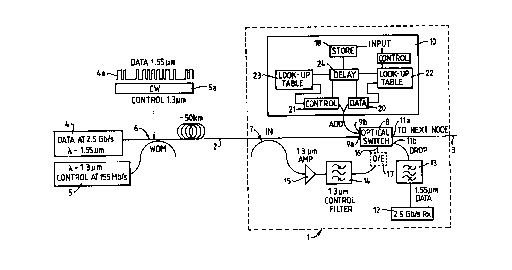
Referring to the drawings, Figure 1 shows one node 1
of a packet switching optical fibre network, the.network
including a plurality of similar nodes. The node 1 is
connected to the network via input and output fibres 2 and 3
re~pectively. The input fibre 2 is connected to a head-end
station (not ghown in detail) provided with an optical data
30 generator 4 and a header generator 5. The optical data
generator 4 produces data packets of 16-bit length (one of
which is shown at 4a) by modulating a laser (not shown) at
2.5 Gbit/sec and at a wavelength of l.SS~m. The ~e~er
generator 5 produces header (control) signals (one of which
35 is shown at Sa) by modulating a second laser (not shown) at
an effective rate of 155 Mbit/sec corresponding to data
packets of 16-bit length, and at a wavelength of, for
WO93/21706 PCT/GB93/~747
2123220 - 6 -
example, l.3~m. This modulation is chosen so that the laser
of the header generator 5 is turned on at, or just before,
the start of a data packet 4a, and off at, or just after, the
end of that data packet. The control signal wavelength is
S chosen to match the receive wavelength of the node l, and the
header generator 5 is tunable so as to provide control
signals at different wavelengths, each of which matches the
receive wavelength of another network node. The two signals
4a and Sa are superimposed onto the fi~re 2 by means of a WDM
coupler 6.
The node l includes a four-port optical switch 8 for
adding data to, and dropping data from, the network. The
switch 8 has first and second input ports 9a and 9b
respectively, the first input port being connected to the
lS input fibre 2 via a splitter 7, and the second input port
being connected to a data add module lO (to be described in
greater detail below). The switch 8 has first and second
ou~uL ports lla and llb respectively, the first ouL~u~ port
being connected to the output fibre 3, and the second output
20 port being connected to a 2.5 Gbit/sec receiver 12 via a
band-pass filter l3.
The splitter 7 demultiplexes a small proportion
(typically a few percent) of the control signal Sa of an
incoming packet, and feeds this tapped signal to a band-pass
filter 14 via a l.3~m optical amplifier 15. The filter 14
has a narrow pass band centred on l.3~m, so that it will pass
the tapped signal provided the wavelength of the tapped
- signal matches that of the pass band of the filter. The
o~L~uL of the filter 14 is fed to a control port 16 of the
30 optical switch 8, thereby to open the switch and connect the
first input port 9a to the second output port llb. In this
way, a data pac~et intended for the node l is dropped to its
receiver 12. As the control signal 5a is overlaps the data
signal 4a in the packet, the switch 8 is opened at, or just
35 before, the start of the data reaches the switch and is
clo~ed at, or just after, the end of the data leaves the
~witch. Thus the control signal applied to the control port
W093/217~ 21 2 3 2 2 0 PCT/GB93/00747
-- 7
16 has at least the same time duration as the data packet.
The filter 13 has a narrow pass band centred on a wavelength
of 1.55~m (the data wavelength), so that the signal reaching
the receiver 12 is solely a data signal. The filter 13 not
only filters out the remaining control signal Sa,. it also
filters out noise. If the wavelength of the tapped signal
does not m~tch that of the pass band of the filter 14, the
filter has no output signal and the optical switch 8 remains
closed, that is to say its first input port 9a is connected
10 to its first output port lla. In this way, the data/control
packet associated with the tapped signal is routed through
the node 1 to the output fibre 3 and on into the network.
.he switch 8 is preferably an all-optical switch such
as a non-linear optical amplifier ~NLOA). Alternatively, the
15 switch could be an opto-electronic device such as a lithium
niobate switch, in which case an opto-electronic converter 17
(shown in dashed lines) would be included in the path between
the filter 14 and the control port 16 of the switch 8. The
converter 17 would not reauire any processing capabilities,
20 but would need to carry out a certain amount of amplification
to ensure that a sufficiently large electronic signal is
input to control the switch 8. Simple opto-electronic
components of this type are readily available; and, combined
with known switching technology, can produce switch rise and
fall times of much less than lns.
The module 10 of the node 1 can add data packets onto
the network when either a packet has been d~o~cd by the node
(having been triggered by the header address decoder
de~cri~ed above), or if some protocol (~uch as a token-ring
30 type protocol) allows input onto an empty line whilst
engurins controlled and fair networ~ access. Data packets
for transmission in this way are held in a memory store 18
provided in the module 10. The module 10 also includes an
optical ~e~er generator 20 and a data generator 21. The
g~nerators 20 and 21 are tunable so as to transmit data at
any one of a plurality of predetermined wavelengths, and to
transmit control signals at any one of a plurality of
WO93~21706 PCT/GB93/00747
~ 123220
different wavelengths. ~espective loo~-up ~tables 22 and 23
are associated with the data and header generators 20 and 21
respectively, so that the wavelengths of both the data and
the control signals for the required destination of a given
5 packet are correctly provlded. If dispersion is a potential
problem, the look-up tables 22 and 23 can work out the
difference between the transmission times of the control
signal and the data signal so chosen, and can instruct a
delay unit 24 to provide an appropriate delay between the
10 transmission start times of the control and data signals,
thereby to ensure that the control signal Sa completely
overlaps the data signal 4a at the destination node, thereby
ensuring that its optical switch 8 routes the whole of the
data signal and does not lose any data bits. The loss of
15 data bits wo~ld cause errors, and thereby detract from the
operational characteristics of the network.
The head-end station also includes a memory store,
iook-up tables and a delay unit (similar to the items 18, 22,
23 and 24 of the module 10), so that data for transmission
can be held awaiting transmission, the data and header
wavelengths for transmission to any given node of the network
- can be worked out, and an appropriate de}ay can be provided
in the transmission store times in the header and data
signals for reaucing dispersion problems. Indeed, the head-
end station may include a data add module of the same type as
that provided at the node 1. It would also be possible to
provide the node 1 (and any other similar node connected to
the network) with a tunable filters 13 and 14 so that the
wavelengths of the control and data signals appropriate to
30 each of the nodes can be altered, for example by a management
centre, if required. In this case, it would be possible for
the head-end station to be identical to each of the nodes 1
in the network.
Because of changes in the effective optical path
3S length of network links caused by environmental alterations,
such as temperature, the delay between any pair of nodes
alters. This alteration could result in loss of information
wo 93/21706 2 1 2 3 2 2 0 PCT/GB93/00747
at the destination node 1, due to the control signal 5a
moving with respect to the data signal 4a. This change in
optical path length will probably only occur on time scales
no greater than the kHz level. In order to ensure that all
the optical path lengths are known and that the network
~emains "synchronised~ (that is to say the control signals 5a
overlap the data signals 4a at all the nodes 1), feedback
information between the node~ is needed to monitor optical
path lengths, and to adjust the look-up tables 22 and 23
10 accordingly. This feedback signal can be achieved by
monitoring the arrival of the control signals 5a at-the nodes
1. Thus, if the network knows where the information has come
from (by monitoring the fibre that the signal arrived on),
and monitors the relative time that a given control signal Sa
lS is incident on the node, then any differences in path delay
can be monitored. As shown in Figure 1, this monitoring can
be achieved by providing the look-up tables 22 and 23 of each
node 1 with local processors 22a and 23a, and by tapping off
a small percentage of the output signal of the filter 14 of
each node 1 to a further local processor 14a. The processor
14a of a desti~ation node 1 determines what has happened to
the network, and sends a suitable update control signal
through the network to all the other nodes to tell them how
to update their look-up tables 22 and 23. These update
25 signals may go via a central management centre (not shown)
provided at the head-end station, or via some other
management centre, perhaps lin~ing a sub-set of the nodes 1.
The need to provide a management centre depends on whether
the total proce~sing time of the local processors 22a, 23a
30 and 14a is sufficient to make sure that the network stays
~stable~, and that the update control signals do not cause
problems by changing the network after it has naturally
recovered to its normal state (or it is still responding to
previous signals). In other word~, the time taken to adjust
35 the network should be at most egual to the time-constants of
the perturbing effects.
The local processors 22a and 23a in each of the
:~ '
WO93/217~ PCT/GB93/00747
2123~2U - lo-
.
transmission nodes 1 receive update control information from
every other node in the network, and process this to modify
their associated look-up .a~les 22 and 23 correctly. Thus,
the look-up tables 22 and 23 of all the nodes 1 (including
the head-end station) are continually up-dated to compensate
for environmental alterations. The degree of intelligence
that the local management processors 22a and 23a have will
dictate the strategy for the look-up table upgrade. Thus, it
would be ideal if the ~rocessors 22a and 23a look at a num~er
of inter-dependent signals to work out the best solution for
the network as a whole, covering all the links that the
information t-averses on lts way to a given destination. The
capability neeaed is, therefore, related to the number of
nodes 1 in the ne~work.
The viability of the coding/decoding apparatus (and in
particular the viability of using an NLOA as the optical
switch 8) described above with reference to Figure 1 has been
tested experimentally using the configuration shown in Figure
2. A data signal 4a a~ a wavelength of about 1.55~m (1.535~m
20 to 1.56~m operational range) was modulated at 1 Gb/s to 2.5
Gb/s. The control signal _a was a 1.31~m DFB laser modulated
with 1010 pattern at lJ16th the bit-rate of the data. These
signals 4a, 5a were injected into the absorber facet 8a of a
bulk materiai NLOA 8 which was under st~n~Ard bias
conditions. Improved performance occurred when the a~sorber
bias was reduced. The output from the NL~A 8 was filtered
uging a band-~ass ~ilter 13 at the data wavelength. Typical
gated data signals are shown in Figures 3a to 3d. These
re~ults are for 1 GbJs data, but identical behaviour was
ob~erved at speeds of 2.5 ~b/s. NLOAs operating at >5 Gb/s
haYe been demonstrated, and further speed improvements are
expected with device optimisation.
Operation in two modes (resonant amplifier and
inj ection locked ) has ~een demonstrated. The resonant
amplifier mode results are shown in Figures 3a and 3b, while
those for the injection locked case are shown in Figures 3c
and 3d. The measured extinction ratio for both cases was >13
WO93/21706 21 2 3 ~ 2 0 PCT/GB93/00747
dB ~etween the ~ated data and the rejected data signals, and
the EYE diagram shows a clean opening and good error-ratio
performance is expected. The contrast ratio (the on-level
power relative to the off-level power referenced to 0) was
>10 dB. The -ise and fall of the gate for the resonant
amplifier case was - 2-5ns, and dependent on the detuning of
the data wavelength from the NLOA Fabry-Perot mode. A
detuning range of - 10 GHz was possible which would require
wavelength referencing in a network configuration to ensure
good performance.
In the injection iocked mode (NLOA almost or .at
threshold), the rise and 'all times were less than a bit-
period (400ps), but the network benefits of this faster
gating time are Dalanced by a much tighter detuning
requirement, with successful operation obtainable over a data
wavelength range of approximately 1-2 GHz.
The technique described above can be used in packet,
virtual and circuit systems. It maintains a transparent data
ch~nnel, and puts the necessary bit-rate specific information
(such as packet duration, required rise and fall times etc)
into a control channel at a different wavelength. The
principle of the invention could also be used in ~frameU
systems, such as synchronised digital hierarchy (SDH) where
the data ~it-rate is se~, and to fast circuit switched
25 networks. The technique could also be used for distribution
applications for data communications networks in LAN, MAN and
WAN environments, and the general principle may also be used
in trunk applications if configured correctly.
The technique can be used in ring, star and star/ring
30 topologies as described below with references to ~igures 4 to
6. Thus, Eigure 4 shows one possible configuration for using
the wavelength header coding/decoding technique of the
invention in a simple ring network. This network include~
four nodes 31, each of which is similar to the node 1 of
Figure 1. The nodes 31 are connected in a ring configuration
at the end of a trunk spur 32. Each of the nodes 31 has a
different address wavelength Al, A2, A3 and Al which matches
W093/21706 PCT/GB93/00747
2123220 - 12 -
the control signal waveleng~hs input by the trunk spur 32.
Obviously, therefore, the filters 14 of the nodes 31 are
different, each having a narrow pass band centred on the
appropriate address wavelength Al, A2, l~ or A4.
S Data from the networ~ enters the ring via ~he trunk
spur 32 and a trunk multiplexer (such as a 3dB coupler) 33,
and travels around the ring reaching each of the nodes 31 in
turn. At each node ~1, the information on the line is
interrogated and, when the control signal 5a of any given
10 packet matches the address wavelength of a node, the data is
routed off the ring, and local data ready for transmis~ion
into the network ~an be added in its place. As with the
embodiment of Figure 1, there is an add~drop function at the
wavelengths of bot~ data and control signals. Data
circulating in the ring is multiplexed back onto the trunk
spur 32 after travelling completely around the ring. Thifi
type of configuration could, therefore, be useful for
signalling networks with the transfer of control information
between nodec.
Information entering and leaving the ring doe~ not
neces~arily need to be at the same wavelength or bit-rate if
the trunk multiplexers are designed correctly. For example,
if the trunk network is a wavelength routed network (at the
data wavelength) then outward information can be transmitted
25 at any of the available network wavelengths. The control
~ignal wavelengths can, therefore, also be any convenient
value. Although Figure 4 shows only four nodes 31 on the
ring, it wiIl be apparent that the principle can be exten~e~
to virtually any number of~nodes, this number being dlctated
30 by factors such as the control wavelength range, the filter
bandwidth, the pass bandwidth of the wavelength-routed cross-
con~ects elsewhere in the network, and any dispersion
problems. As mentioned above, each of the nodes 31 includes
an a~plifier for amplifying the tapped signal, so that a very
35 low percentage of an input signal needs to be tapped, 80 that
many nodes can be concatenated.
Figure 5 shows a star topology network having five
W093/21706 2 12 ~ 2 2 0 PCT/GB93/00747
- 13 -
.
~ rings 40 each of which is similar to the ring described above
with reference to ~igure 4. Each ring 40 includes four nodes
41, each of which is similar to the node 1 o~ Figure 1. Each
of the rings 40 is connected to a wavelength routed cross-
connec~ 43 via a respective trunk spur 42. Each of the trunk
spurs 42 is arranged to carry data at a respective data
wavelength Ad,~,l, A~",2, A~",3, A~",l and Ada"s. ' Each of the
nodes 41 of each ring 40 has different address wavelength A
to A~o which matches the header wavelengths input ~y the trun~
spurs 42. Here again, the filters 14 of the nodes 41 are
different, each having a narrow pass band centred on the
appropriate address wavelength A~ to l20.
The wavelength routed cross-connect 43, which
interconnects the five rings 40, ensures that the control
signals are always routed over the same effective path as the
associated data. This cross-connect 43 is shown in detail in
Figure 7, and has the same interconnections for both control
and data fields, any switching within these fields being
driven in synchronism. A node 41 that wants to transmit da~a
20 to another node 41 within the network chooses the correct
data wavelength (for example Ad,~,l) and the correct control
signal wavelength (for example A2). The cross-connect 43 is
desianed to route control signal bands rather than single
wavelengths, that is to say a band of wavelengths Al to A~ is
routed rather than routing each of these wavelengths
separately. This principle could also be used to route the
data wavelengths, which would increase the capacity of the
3rk.
Figure 6 shows a sta~-ring topology having five rings
50, each of which includes four nodes 51, each being similar
to the node 1 of Figure 1. Each of the rings 50 is connected
to an inner ring 54 via a respective trunk spur 52 and a
wavelength routed cross-connect 53. The trunk spurs 52 also
lead to a central wavelength routed cross-connect 55, and
each is arranged to carry data at a respective data
wavelength Ad~ to Ad~l~S- Each of the nodes Sl of each ring
50 has a different address wavelength Al to A20 which matches
WO93/21706 PCT/GB93/00747
212~220 i4 -
the control signal wavelengths input by the trunk spurs 52.
Here again, the filters 14 of the nodes Sl are different,
each having a narrow ~ass band centred on the appropriate
address wavelength A. to A~n. The wavelength routed cross-
connects 53 and 55 are similar to that shown in Figure 7, andensure that the control signals are always routed over the
same effective path as the associated data.
Any switching .hal is required, for contention
resolution or re-ro~ting, at any of the cross-connects 43, 53
and 55 will reauire ~hat an arriving control signal Sa
completely overlaps _n time its associated data signal 4a.
This overlap need only occur within a given switching window.
The control of the look-up tables 22 and 23 of the
transmitting node wii; need to take this into account when
lS setting up the transmission. The complexity of the networ~
and the choice or waveiengths is, therefore, related. This
is particularly the case where packets are routed through one
or more cross-connects between a transmission node and a
destination node, where t may be escential to ensure
20 overlapping or control and data signals at the cros~-
connect(s) - althougn this may not be required if the cross-
connects are such that the optical switch within the control
cross-connect can operate non-synchronously with respect to
the optical switch within -he data cross-connect.