Note: Descriptions are shown in the official language in which they were submitted.
--` 2~237~
ALL DIGITAL MAXIMUM LIKELIHOOD BASED SPREAD SPECTRUM
RECEIVER
Field of the Inventiol-
The present invention relates generally to communication systems, and more
5 particularly to receivers for use in spread spectrum communication systems.
Related A~t
In the past, direct-sequence spread-spectrum techniques have not been widely
used due to their relatively high cost. However, the recent development and use of
custom digital VLSI (very large scale integration) techniques have made the cost of
10 spread-spectrum signal processing affordable. Consequently, direct-sequence spread-
spectrum techniques have received much attention in the last few years as a viable
technological option for many commercial applications, such as for commercial
portable mobile communication systems.
Conventionally, spread-spectrum transceiver components are implemented in
15 an economic manner using application-specific integrated circuit (ASIC) chips. The
use of ASIC chips in spread spectrum kansceiver components has heretofore been
deemed necessary due to the rather unique signal processing requirements associated
with spread spectrum comrnunication. In particular, in a spread-spectrum receiver, the
design philosophy is to tolerate interference. Designing to tolerate interference results
20 in a higher quality radio, and can lead to an increase in the network capacity. As will
be appreciated, such design philosophy associated with spread-spectrum receiversgenerally differs from the design philosophy employed when developing conventional
narrowband radios.
As a result of the rather unique signal processing requirements associated with
25 spread spectrum comrnunication, in the past it has not been possible to employ
standard digital signal processing techniques when developing spread-spectrum
receivers. This represents a disadvantage of conventional spread-spectrum receivers,
since digital signal processing techniques offer the ability to employ powerful signal
~ . . .
-` 2~2373~ ~
conditioning and processing algorithms that give rise to robust receivers.
Consequently, generic, general purpose spread spectrum digital signal processors (DSP)
do not currently exist.
.
Summsry of the Invention
The present invention is directed to a spread spectrum receiver for use in a
spread spectrum communication system. The receiver of the present invention includes
an analog-to-digital converter for receiving an analog spread spectrum signal, and for
converting the received analog signal to a digital signal. The received analog signal
includes a plurality of main and multipath return signals of varying signal strengths.
10 The spread spectrum receiver also includes a Rake receiver, and a frequency offset
correction device, coupled to the analog-to-digital converter, for modifying the digital
signal in accordance with a frequency correction term signal to thereby correct for
frequency offset in the received analog signal.
The spread spectrum receiver searches through the modified digital signal to
15 identify M of the main and multipath return signals having the strongest signal
strengths. The identified main and multipath return signals are processed in
accordance with predetermined maximum likelihood techniques to thereby generate the
maximal-ratio-combining weighting factor, carrier phase correction term, and thefrequency correction term signal.
Further features and advantages of the present invention, as well as the
structure and operation of various embodiments of the present invention, are described
in detail below with reference to the accompanying drawings. In the drawings, like
reference numbers indicate identical or functionally similar elements.
Brief Description of the Fi~ures
The present invention will be described with reference to the accompanying
drawings, wherein:
Figure 1 is a structural block diagram of a spread spectrum receiver in
accordance with a preferred embodiment of the present invention;
,, . ~. . . .. .
212373~
Figure 2 is a structural block diagram of a preferred computation unit of the
present invention;
Figure 3 is a more detailed structural block diagrann of a portion of the spreadspectrum receiver of Figure l;
Figures 4A and 4B collectively illustrate a flowchart depicting the preferred
detailed operation of the spread spectrum receiver of the present invention;
Figure 5 is a structural block diagram of a noncoherent peak detector in
accordance with a preferred embodiment of the present invention;
Figure 6 is a structural block diagram of a correlator in accordance with a
10 preferred embodiment of the present invention; and
Figure 7 illustrates a flowchart depicting the preferred general operation of the
spread spectrum receiver of the present invention.
Detailed DescriDtion of the Preferred Embodiments
1. Overview of the Present Invention
The present invention is directed to a completely digital, preferably MPSK
(multiple phase shift keying) direct-sequence spread-spectrum receiver. The spread
spectrum receiver of the present invention is preferably used with CDMA (Code-
Division Multiple Access) cellular and cordless telephone applications, although the
spread spectrum receiver of the present invention is adapted for use with other types
20 of communication applications.
Preferably, the spread spectrum receiver of the present invention is
implemented using various digital algorithrns for phase estimation, frequency
estimation, Rake diversity combining, and PN (pseudo noise) code tracking based on
maximum likelihood (ML) principles. These algorithms have a low numerical
25 complexity and a computational structure that results in a very regular receiver
architecture.
r
,~ i h'J ~ cJ-~
- 4 -
2. Description of th~ii~Received bY the Spread SPectrum Receiver
The complex analog signal which is transmitted to and received by the spread
spectrum receiver of the present invention is described in this section. The manner in
which this complex analog signal is generated and transrnitted to the spread spectrum
. 5 receiver is also described in this section.
Spread-spectrum communication is described in many publicly available
-~ documents, such as Di~ital Communications by Proakis (New York, McGraw Hill,
1989) and S~read-Spectrum Communications by Simon et al. (Computer Science Press,
1989). As is well known, spread spectrum communication signals used for the
transrnission of digital information are characterized by their large bandwidth W, which
is much greater than the information rate R in bits per second. Thus, the bandwidth
expansion factor L = W~ for a spread spectrum signal is much greater than unity.The large redundancy inherent in these signals is required to overcome the severe
levels of interference that are encountered in the transmission of digital information
over some radio and satellite channels. In addition, the pseudo-random structure of
the signals makes them appear similar to random noise and difficult to demodulate by
receivers other than the intended ones.
Direct-sequence spread-spectrum (DS-SS) modulation is generially well known.
In DS-SS, a carrier is modulated first by a pseudorandom waveforrn, also called
pseudo noise (PN) waveform, before modulation by a data stream. The PN waveform
consists of a sequence of bits (called chips), each of duration Tc < Th (where
Tc = pedod of one chip, and Th = period of one symbol, or baud). Usually, one bit
period contains up to severial hundred chips. The transmitted direct-sequence spread-
spectn~m signal s(t) can be written as follows:
s(t) = ~ d (t) c(t) e~f
where
~ -: : :: : . :
212373~
~i d (t`J = ~ d" p, tt-kTb)
and
C(t) = ~ C~p2(t~ T~)
dk takes on values fe'2J0"M~, where 0 < m 5 M-1 (for M-ary PSK), with symbol period
Tb seconds. ~O denotes the carrier frequency, Es is the signal energy, and ck is a +1-
valued, L-chip-long spreading (PN) code with chip time Tc = TJL seconds. The
S original data spectrum is thus spread out in frequency by a factor of L, resulting in a
spread-spectrum signal. The process of multiplying the transrnitted data by the PN
code is conventionally called spreading the signal. The waveforms pl(t) and p2(t) are
a rectangular pulse waveform and a chip pulse-shaping waveform.
The signal passes through a fading multipath channel which is described in
10 many publicly available documents, such as "Introduction to Spread-Spectrum
Antimultipath Techniques and Their Applications to Urban Digital Radio" by Turin(Proc. EEE. vol. 68, pp. 328-353, 1980), which is herein incorporated by ref r(t),
which is received by the spread spectrum receiver of the present invention, is acomplex analog signal. After demodulation (not phase-locked), the signal r(t) is15 represented as follows:
r(t) ~ hl(t) ~ d(f-~l-E~Tc) c(t-~l-E,T e3(2~ 0 + n(t)
...
where ~f is the frequency offset, ~ is a random initial phase, n(t) represents noise plus
any other interference introduced through the channel, arld ~TC is the received code
offset with respect to an arbitrary time reference. The complex fading process on the
-" 21'i'~73~
- 6 -
i~h multiple path is characterized by the complex phaser h(t) = oc~ , where aj and
can vary slowly with time. The delay of the irh channel is characterized by ~,.
3. StFucture and Operation of the .~r read SPectrum Receiver
The structure and operation of the spread spectrum receiver of the present
5 invention shall now be described in detail.
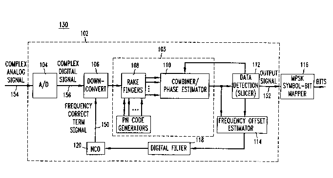
Figure I is a block diagram of a spread spectrum receiver 102 in accordance
with a preferred embodiment of the present invention. The receiver 102 includes an
analog to digital (A/D) converter 104, a down converter 106, a Rake receiver 103, and
a data detection device (also called slicer) 112. The slicer 112 generates an output
10 signal 152 which is transferred to a MPSK symbol-to-bit (symbol-bit) mapper 116,
which is not part of the receiver 102 of the present invention. The Rake receiver 103
includes M Rake fingers 108 (also called Rake arms), pseudo noise (PN) generators
122, and a multipath diversity combiner/phase estimator 110.
The receiver 102 also includes a digital feedback loop 130 which operates to
15 generate a signal 150 representing a frequency correction term. The frequencycorrection terrn signal 150 is transferred to the down converter 106, as furtherdescribed below. The digital feedback loop 130 includes a frequency offset estimator
114, a digital filter 118, and a digital numerically controlled oscillator (NCO) 120.
Figure 3 is a more detailed block diagrarn of a portion of the receiver 102. In
20 particular, Figure 3 illustrates in block diagram form the structure and data flow
characteristics of the Rake fingers 108, the multipath diversity combiner/phase
estimator 110, and the PN code generators 122. Also shown in Figure 3 is the slicer
112, the frequency offset estimator 114, and the MPSK symbol-bit mapper 116.
The operation of the spread spectrum receiver 102 of the present invention shall25 now be described with reference to Figure 7, which illustrates a flowchart 702
depicting the operation of the present invention. The flowchart 702 begins with step
704, where control immediately passes to step 706.
In step 706, the analog to digital (A/D) converter 104 receives a complex
analog signal 154 (described above). The A/D converter 104 converts the complex
2 1 2 ~ ~ 3 ~
analog signal 154 to a complex digital signal 156. Step 706 is further described in a
subsequent portion of this document with reference to step 406 in Figures 4A and 4B.
As will be appreciated, the frequency of the signal received by the receiver 102may be offset from the frequency of the signal originally transmitted. This frequency
5 offset may be due to a number of reasons. For example, the frequency offset may
result if the reference frequency at the receiver 102 differs from the re~erencefrequency at the transmitter (not shown). The frequency offset may result if thereceiver 102 or transmitter (not shown) is moving through space, thereby creating a
doppler frequency offset. Also, the frequency offset may be due to drift in the
10 reference frequency oscillator (not shown) of the receiver 102.
In step 708, the downconverter 106 receives the complex digital signal 156, and
modifies the complex digital signal 156 to correct for frequency offset in the signal
received by the receiver 102. Preferably, the downconverter 106 perforrns frequency
offset correction by modifying the complex digital signal 156 using a frequency
` 15 correction term signal 150 generated by a digital feedback loop 130 (described below).
Step 708 is further described in a subsequent por~ion of this document with reference
to step 408 in Figures 4A and 4B.
The local PN code generators 122 must be synchronized with the phase of the
incoming code. Such synchronization requires both acquisition and tracking systems
20 in order to rapidly acquire.an unknown code phase, and then track the code phase to
within a fraction of a chip. Acquisition is preferably performed using a multipath
search algorithm (described below), which is preferably implemented using one of the
Rake fingers 108. Preferably, Rake finger 309 is used. Rake finger 309 is hereinafter
referred to as the acquisition Rake finger 309.
Accordingly, in step 710, the receiver 102 determines whether to enter an
acquisition mode or a tracking mode. It is noted that synchronization and all
subsequent operations significantly suffer in the presence of any large frequency
offsets. Thus, before performing step 710, the receiver 102 performs step 708 wherein
the downconverter 106 compensates for any possible frequency offset in the received
-- 2~ 237~
- 8 -
signal (as described above). Step 710 is further described in a subsequent portion of
this document with reference to step 412 in Figures 4A and 4B.
If, in step 710, the receiver 102 decides to enter the acquisition mode, then step
712 is perfonned. In step 712, the acquisition Rake finger 309 in conjunction with the
5 PN code generators 122 searches for the code phase of the received signal by
searching for the M strongest main and multipath returns of the received signal. A
correlation operation is preferably utilized to perform step 710.
More particularly, in step 710 the receiver 102 estimates the M strongest main
and multipath returns of the received signal. This involves observing the received
10 signal over a period of time, which is preferably W chip-periods in duration, and
selecting the M signal paths based on the signal strength. The result of this estimation
procedure is a list of ordered pairs Ti, &i, corresponding to the receiver's estimate of
the actual multipath delays ~i, and their relative weights ai, where i=1,2,..M. The
receiver 102 then uses these ~, estimates to drive M code generators, which feed the
15 Rake fingers 108, thereby despreading the aggregate received signal M times, each
Rake despreading arm (or fingers) corresponding to a different code phase. Step 712
is further described in a subsequent portion of this document with reference to steps
414-418 in Figures 4A and 4B.
If, in step 710, the receiver 102 decides to enter the tracking mode, then the
20 series of steps beginning with step 714 are performed. These steps are also performed
after step 712 is performed.
Code tracking is performed during step 714. Specifically, in step 714, the Rake
fingers 108 continuously maintàùn the best possible waveform alignment by means of
a closed loop operation. Specifically, each of the M Rake fingers 108 tracks the25 respective code to within a fraction of a chip. Step 714 is further described in a
subsequent portion of this document with reference to step 420 in Figures 4A and 4B.
In steps 716 and 718, the receiver 102 modifies the received signal such that
the slicer 112 can make a symbol decision. Preferably, the receiver 102 modifies the
received signal in this manner using maximum likelihood techniques. Specifically, in
30 step 716 the combiner/phase estimator 110 uses maximum likelihood techniques to
. . . ~ . -
. . .~ ~ :: . .
212373~
- 9 -
estimate carrier phase estimates and maximal-ratio combining weighting factor
estimates. In step 718, the combiner/phase estimator 110 uses the carrier phase
estimates and weighting factor estimates to modify the received signal such that the
., slicer 112 can make a symbol decision. Steps 716 and 718 are further described in a
subsequent portion of this patent document with reference to steps 426 and 428 in
Figures 4A and 4B.
In step 720, the slicer 112 processes the signal produced by the combiner/phase
estimator 110 and makes a symbol decision. Step 720 is further described in a
subsequent portion of this patent document with reference to steps 430 and 438 in
Figures 4A and 4B.
In step 722, the frequency offset estimator 114 uses maximum likelihood
techniques to generate a carrier frequency offset estimation using the signal produced
by the combiner/phase estimator 110. This carrier frequency offset estimation isprocessed by the digital filter 118 and the NCO 120 and is transferred to the
downconverter 106, which uses the processed carrier frequency offset estimation (also
called the frequency correction tenn signal 150) to correct for frequency offset in the
received signal (discussed above in step 708). Step 722 is further described with
reference to steps 432-436 in Figures 4A and 4B.
The operation of the spread spectrum receiver 102 of the present invention shall ~;~
now be described in greater detail with reference to Figures 4A and 4B. Figures 4A
and 4B collectively illustrate a flowchart 402 depicting the operation of the present
mvenhon. ~ '
The flowchart 402 begins with step 404, where control imrnediately passes to
step 406.
In step 406, the analog to digital (A/D) converter 104 receives a complex
analog signal lS4 (described above). As is well known, complex signals may be
represented in the digital domain as in-phase and quadrature components, or as
amplitude and/or phase components. It often proves useful to convert between the two
while performing certain functions (see Viterbi et al., "Nonlinear Estimation of PSK-
Modulated Carrier Phase with Application to Burst Digital Transmission," IEEE Trans.
2123735
- 10
on Info. Theory, pp. 543-551, 1983). For illustrative purposes only, the complexsignals discussed herein are considered using the l/Q (in-phase/quadrature) signal
representation unless stated otherwise.
The A/D converter 104 converts the complex analog signal 154 to a complex
S digital signal 156. Specifically, the A/D converter 104 over-samples the I/Q signals
154 at preferably several times chip rate. In accordance with the Nyquist theory, the
minimum sampling rate required to accurately bring the analog spread-spectrum signal
154 into the digital domain is 2/TC (i.e., 2 samples per chip period).
The complex digital signal 156 generated by the A/D converter 104, and which
10 is eventually received by the Rake fingers 108 (after processing by the downconverter
106), can be written as follows:
D
r(k) = h~(kTs) ~ d(kTs~ TC) c(kTs~ Tc~ i(2~TJ + n(kT3)
Preferably, symbol decisions are made on the output of the Rake fingers 108
at the symbol rate Tb. From the A/D converter 104 to the output of the Rake fingers
108, the sample rate is preferably at M~c~ whereas after the Rake fingers 108 the
15 sample rate is preferably at l~rb, the symbol rate.
In step 408, the downconverter 106 receives the complex digital signal 156.
The downconverter 106 is responsible for automatically controlling the frequency of
the complex digital signal 156. In other words, the downconverter 106 performs
frequency offset correction. Preferably, the downconverter 106 performs frequency
20 offset correction by modifying the complex digital signal 156 using a frequency
correction term signal 150 generated by the digital feedback loop 130 ~describedbçlow). Preferably, the downconverter 106 complex multiplies the complex digitalsignal 156 using the frequency correction term signal 150 to perform frequency offset
correction.
In step 410, the output signals from the downconverter 106 are transferred to
each of the Rake fingers 108. As best shown in Figure 3, each of the Rake fingers
~12373~
108 comprises a multiplier 312 and an integrator 306, the combination of which is also
called a correlator.
Rake communication systems and components are generally well known, and
are described in many publicly available documents such as "Introduction to Spread-
S Spectrum Antimultipath Techniques and Their Applications to Urban Digital Radio"
by Turin, referenced above. The Rake receiver 103 of the present invention is sirnilar
to conventional Rake receivers, except that the Rake receiver 103 of the presentinvention operates with feed-forward and feedback estimators 114 and 310. Also, the
Rake receiver 103 is preferably implemented with all digital components. As noted
above, one finger 309 of the Rake receiver 103, comprising a multiplier 314 and a
correlator 308, is reserved for code synchronization operations. Specifically, this
acquisition E~ake finger 309 performs multipath search and acquisition operations. The
operation of the Rake receiver 103 is further described below after first considering
Step 412.
Step 412 is performed after the output signals from the downconverter 106 are
transferred to the Rake fingers 108 in step 410. In step 412, a synchronization mode
is entered. In accordance with a preferred embodiment of the present invention, the
process of synchronization is accomplished in two stages: a code acquisition stage and
a code tracking stage.
When power is first applied to the receiver 102, the controller deterrnines thatreceiver 102 should enter the code acquisition stage. Once the received PN sequences
are aligned with the local PN sequences to within a small relative timing offset (such
alignrnent is described below), the controller determines that the Rake finger
corresponding to the selected code phase should enter the code tracking stage. As long
as such alignment is maintained over M fingers, the overall receiver 102 stays in the
code tracking stage. If such alignment is loss, the controller determines that receiver
102 should re-enter the code acquisition stage.
Systems and methods for deterrnining whether to enter an acquisition mode or
a tracking mode are well known, and any of these well known systems and methods
may be used in conjunction with the receiver 102 of the present invention. Preferably,
.;,.............. . .
1237~
- 12 -
the controller determines whether to enter an acquisition mode or a tracking mode as
follows.
~ When the receiver 102 is turned on, one correlator 309 is used in conjunction
.~, with a search algorithm (described herein) to search for code phases that correspond
' 5 to different multipaths. Based on threshold testing output by the correlator, the
controller either sets a Rake finger into acquisition mode or tracking mode. Once in
tracking mode, a second threshold test, together with an averaging process, is used to
determine whether to stay tracked or return to acquisition mode.
d If, in step 412, the controller determines that the receiver 102 should enter the
acquisition mode, then steps 414-418 are performed. During the acquisition mode (that
7 iS, during the processing of steps 414-418), the acquisition Rake finger 309 aligns the
' received PN sequences ~that is, the PN sequences originally contained in the complex
analog signal 154) with local PN sequences generated by the M PN code generators302. The received PN sequences are aligned with the local PN sequences to withina small relative timing offset, preferably less than a fraction of a code chip.
More particularly, during the acquisition mode the acquisition Rake finger 309
interacts with the PN code generators 122 to estimate the M strongest paths. This
involves observing the received signal r(t) 154 (as processed by the A/D converter 104
and the downconverter 106) over a period of time (preferably W Ghip-periods in
duration), and selecting the M signal paths based on the signal strength. The result of
this estimation proceclure is a list of ordered pairs ('c" O, corresponding to the
acquisition Rake finger 309's estimate of the actual path delays ~j and their relative
weights al where i=1,2,...M. During this process, the acquisition Rake finger 309
operates in a multipath search mode and a freeze mode.
Steps 414-418 shall now be described in detail.
In step 414, the controller (not shown) employs a multipath search algorithm
(described below) to generate M code phase offsets. These M offsets are fed to M PN
code generators 302. Specifically, during step 414, the acquisition Rake finger 309
operates in a multipath search mode. During the multipath search mode, the PN code
generator 302 associated with the acquisition Rake finger 309 selects a reference phase
21~73~
- 13 -
o (that is, the code phase corresponding to the main received path), and tests the code
phases ~0 + k~. k varies over the values 1,2,...WT~I~, so that a window of delays
up to duration W chip periods is covered. For each delay value tested, the acquisition
Rake finger 309 dwells on this phase for several chip periods. The value generated
5 by the acquisition Rake finger 309 is first threshold compared, and then compared to
the delays that yielded the M largest signals. The M largest delays ~i are stored in a
random access memory (RAM), not shown. This continues for all WT~ values of
k (chosen by the search algorithm). Steps 416 and 418 pertain to stepping through the
possible values of k.
In step 416, the multipath search logic/PN generator 304, 302 generates codes
with different offsets, and then uses these codes to search for strong signal returns
from the output of the acquisition Rake finger 309. In order to test a possible code
phase position, exactly DTC seconds are required. D is a predetermined,
implementation dependent, integer value. At the end of DTC seconds, the result in the
acquisition Rake flnger 309 is dumped to a register 608 (see Figure 6). At this point,
DTC seconds of the received signal has been lost to the receiver 102. The next value
of delay 'c, that is tested uses the next DTC seconds of the signal. Which values of 'ci
that are tested depends on the search strategy (as described above), which is preferably
microcoded. The only signal processing hardware necessary to perform step 416 is the
acquisition Rake finger 309, with some associated control logic to implement thesearch strategy. Only the M delays 'ci that yielded the largest correlations are stored
in RAM. As a result of step 416, the PN code generators 302 for each Rake arm have
the code timing information necessary to generate a local code with the proper code
phase so that M-branch processing and multipath combining can take place.
In step 418, the M largest multipath delays are selected and the M code
generators 302 are frozen in time (that is, are placed in the freeze mode). In the freeze
mode, the search circuitry may be shut down to save power. Specifically, during step
418, the delays ~, from step 416 are used to drive the M code generators 302 to
generate local PN code sequences. These local PN code sequences are feed to the
212~73
- 14 -
Rake fingers 108. This results in despreading the aggregate received signal M times,
wherein each Rake despreading finger 108 corresponds to a different multipath delay.
If, in step 412, the controller detennines that the receiver 102 should enter the
tracking mode, then the series of steps starting with step 420 are perforrned. These
5 steps are also perforrned after step 418 has been completed.
Code tracking is performed during step 420. Specifically, in step 420, the Rake
fingers 108 continuously maintain the best possible waveiforrn alignment by means of
a closed loop operation. Specifically, each of the M Rake fingers 108 tracks therespective code to within a fraction of a chip.
Any well known code tracking system and/or method can be used to perform
step 420 of the present invention. Preferably, however, code tracking in step 420 is
performed using a tracking circuit in combination with a noncoherent peak detector
502. The tracking circuit comprises a threshold detector 307 in each of the Rakefingers 108.
Figure 5 is a block diagram of the peak detector 502. The peak detector 502
includes a non-coherent I/Q correlator 522, which has three inputs. The I/Q correlator
522 represents the multiplier 3141integrator 308 combination in the acquisition Rake
finger 309. A LOCAL_CODE signal is generated by the code generator 302 and
represents a locally generated replica of the received code, accurate to within TC/2.
LGCAL_CODE has l-bit samples spaced TC apart. A RX_SIG signal represents the
received signal, and is stored in RAM (not shown) as two B-bit samples (I,Q) spaced
l/TC apart. A INT_DUMP signal is a binary waveform that provides timing
information on when to begin the integration operation and when to dump the result
(latch) into a register (not shown).
The output of the peak detector 502 is a statistic, S~ + S~, which is the sum ofthe squares of the in-phase and quadrature correlator outputs. In the tracking mode,
the Rake receiver 103 picks one of the M possible fractional-Tc phases of the received
signal that corresponds to a peak out of the noncoherent peak detector 502. This peak
appears every symbol period. When the tracking circuit is locked to the correlator
output peaks, a window is used by the detector 502 to select decision samples and to
:
2~ ,~J~73~
- 15 -
. thus derive the code sequence tirning so as to make small tracking corrections to a
. code sequence generator clock (not shown), if necessary. Within the window, a
'i threshold test is perfonned by the threshold detectors 307 using adaptive threshold
controls, and the result of the threshold test is used to either select another timing
. 5 phase or to keep the timing phase unchanged.
A tracking circuit employing a noncoherent peak detector is further described
in "Synchronization Systems for Spread-Spectrum Receivers" by Subramanian (Ph.D.Thesis, EECS Department, University of California, Berkeley, 1991), which is herein
incorporated by reference in its entirety.
Referring again to Figures 4A and 4B, in step 422, the ou~put signals from the
Rake fingers 108 are decimated (that is, the sampling rates are changed) to symbol rate
spaced samples by the samplers 350.
In step 424, the output signals from the samplers 350 are transferred to the
maximum likelihood (ML) phase and weighting factor estimators 310. The output
15 signals from the samplers 350 are also transferred to the multipliers 316.
In step 426, the ML phase estimators 310 each produces a carrier phase and a
weighting factor for one of the M Rake fingers 108. During step 426, the receiver 102
of the present invention weights and coherently combines each of the despread Rake
fingers 108. In order to coherently combine, the receiver 102 estimates the phase of
20 the received signal, ~; in the ia' multiple path to produce ~, which represents the
carrier phase. In order to weight the signal, a maximal-ratio combining rule is used.
Here, each Rake channel arrn 108 (or finger) is weighted according to the gain, oci, in
that channel. Hence, channel i is weighted by ~c,.
The opeMtion of the receiver 102 during step 426 shall now be described in
25 greater detail.
To coherently receive a signal, the carrier phase must be estimated for each
Rake finger 108 before combining. Consider the phase vector ~ 2,...,~L) and
the attenuation vector a = (al,a2,...,aL). The optimum receiver maxirnizes the
conditional probability density function (p(~ I ak, ~,Q~ which is the likelihood30 function for a particular observation _ = (r,(t),r2(t),...,rL(t)) over an observation interval
2 1~62-373~
(see Digital Comrnunications by Proakis, cited above). Consider N observations (i.e.
N samples) of the received signal in an observation interval. The present invention
assumes that the channel is time-invariant over the observation interval spanning
several symbol periods, and the components of the phase vector ~i are mutually
S independent.
Under these assumptions, each of the ML phase estimators 310 obtains (~) of
by solving L(~) = ma~s {L,(0~} where t~) denotes the set of all possible values~
can take on.
This yields the following solutions for cos() and sin() at time k:
) = A ,~;~;~ a~ ~ Re{rl(k)d~(k)}
~-o
10 and
sin(~) = A ~~ a~ {rl(k)d~(k)}}
The constant A shows that the estimate is proportional to cos(~ and S~ f).
A decision-directed scheme, which is performed by the slicer 112 in step 430,
is used to obtain values for d(k), so that the estimate at time k can be based on the
preceding N symbols. This modifies the arguments of the summations above to read
~ Re {r~(k-m)~ (k-m)lJ
~-1
15 and likewise for the imaginary term. Here, a(k-m) denotes the output of the slicer 112
m symbols ago.
Thus, each of the phase estimators 310 generates an estimate of the carrier
phase correction term vj(k) of the forrn:
-~ 2 12 3 7 ~ ~ -
.. .
:
v~0 e'~ = A~- a~ ~0, Re { r~(k)d ~(k)} + jIm { r~(k)d ~(k) }}
E N-l
= A T al ~ r~(k)d ''(k)
at time k.
In step 428, the ML corrected samples are fed to a maximal ratio combiner,
such as multipliers 316, to be weighted. That is, the phase correction and weighting
applied to the received despread signal requires a rotation in the complex plane
S achieved by complex multiplying the signals ri(k) with the signals v,'(k) using the
multipliers 316 in accordance with the following equation:
y~(k) = r~(k) v; (k)
The signals yj(k) represent the output of the multipliers. Also in step 428, the
signals y,(k) are summed in a surnmation device, such as the maximal-ratio diversity
combiner 318, as indicated in the following equation-
z(k) = ~, y~(k)
Step 428 shall now be described in greater detail.
The principle underlying the Rake receiver 108 is maximal-ratio weighting of
the i~ multipath before combining in order to maximize the signal-to-noise ratio of the
output statistic. This is generally discussed, for exarnple, in Di ital Communications
by Proakis, cited above. In order to achieve this, the i'h Rake branch must be ~Iveighted
15 according to the strength of the path, aj. The phase estimators 310 of the present
invention each yields aj as a scaling factor when the complex vector is produced. This
value of al is accurate only as long as the decisions d(k) by the slicer 112 are not in
error since the computations for the phase estimators 310 are performed in a decision
21237~a
- 18 -
directed fashion (as indicated by the feedback line from the slicer 112 to the phase
estimators 310).
Hence, in step 428, the i'h Rake arm 108 is not only rotated, but also weighted
according to its strength, which is exactly what is required for maximal-ratio
S combining. The ML-phase estimators 310 of the present invention generate the
combining factor for earh of the Rake arrns 108, and hence serves as a channel gain
estimator as well. Note that this was possible only because of using planar (i.e., I/Q)
techniques.
In step 430, the output of the sumrnation device 318 is fed to a decision device10 such as a slicer 112. This output of the sumrnation device 318 represents the signal
transmitted from the transmitter (not shown) and received by the receiver 102, as
processed by the A/D converter 104, the downconverter 106, the Rake fingers 108, and
the combiner/phase estimator 110 (as described above). As will be appreciated, the
signal transmitted from the transmitter to the receiver 102is corrupted to some degree
15 by noise. Therefore, the received signal is a corrupted representation of the signal
transmitted by the transmitter.
In step 438, the slicer 112 processes the signal received from the summation
device 318 and makes a symbol decision. As noted above, the received signal is acorrupted representation of the signal transmitted by the transmitter. During step 438,
the slicer 112 essentially makes an estimate as to the symbol content of the received
signal. The structure and operation of slicers are well known, and any well known
slicer could be used in the receiver 102 of the present invention. After performing
step 438, control returns to step 406.
The series of steps beginning with step 432 are also processed after the
performance of step 430 (these steps are preferably processed concurrently with the
processing of step 438). In these steps, the receiver 102 compensa~es for any possible
frequency offset in the received signal. Any frequency offset will manifest itself
idesltically in each Rake arrn 108, since frequency offset is "introduced" prior to the
M-branch signal splitting. The receiver 102 thus needs to estimate any frequency30 offset 4~, and track any slowly varying frequency drifts with a frequency tracking
-` 212~73~
, - 19- : .
system. During step 432, the receiver 102 estimates frequency of~sets ~f. During :
steps 434 and 436, the receiver 102 processes the estimated frequency offsets and
transfers these processed, estimated frequency offsets to the downconverter 106. As
discussed above, the downconverter in step 408 uses the processed, estimated
S frequency offsets to compensate for any frequency offset in the received signal. Steps
432-436 shall now be described in detail.
In step 432, the ML frequency offset estimator 114, which receives the output
of the slicer 112, produces frequency offset error estimates. Step 432 is described in
detail below.
10The frequency offset estimator 114 preferably operates by determining a
maximum likelihood (ML) estimate, and then using the maximum likelihood estimator
to correct the frequency offset. The ML estimate ~f is obtained by solving
L(9J~ = rna~ {L(AF)} where ~f denotes the set of all possible values Qf can take on.
The present invention assumes that ~,fTs~:l. Observations are made on the maximal-
15 ratio-combined Rake output signal since (1) a signal of sufficiently large signal-to-
noise ratio is required, and (2) the effect of a frequency offset ~f is identical in every
arrn. NF sarnples are observed in the estimation observation period.
Taking the derivative of the log-likelihood, and proceeding in an identical
fashion as that described for the phase estimator 310, the estimate Bf is given by:
f(k)T(Np+l)) = ~ Im {z(k-l)d~(k-l)}
iif(~C) T(N~ z(~ )d (~-1) }
20 which can be written as:
N"-l
eJ ~ z(k-l )d (k-l)
1~0
This computation involves an accumulator.
This result can also be written as follows:
, . .
2~2~73~
- 20 -
~ Im ~Z(k-l)d l(k-l) }
3 f( ) 2~Ts(Nf l ) ~ ~-
~ {z(k-l)d~(k-l)}J
This latter form involves an accumulator, a division, an arctangent operation, followed
by another division. Since the possible domain for arctanO ranges from -oo to ~, and
the range is restricted to (-7r~/2,~/2), a table look-up for arctan would be feasible if high
S accuracy is restricted to the range where 4tTs~:l This implies a certain range of
frequency offsets for which the frequency offset estimator 114 produces an accurate
estimate.
As noted above, during steps 434 and 436, the receiver 102 processes the
estimated frequency offsets and transfers these processed, estimated frequency offsets
10 to the downconverter 106. Steps 434 and 436 shall now be described in detail.In step 434, signals representing the frequency error estimates are transferred
to the digital filter 118. The digital filter 118 is used to lowpass filter the frequency
error signal to provide an estimate not heavily corrupted by noise.
In step 436, signals representing the filtered frequency error estimates are
15 transferred from the digital filter 118 to the NCO 120. The NCO 120 uses the filtered
frequency error estimates to produce a frequency correct term. The NCO 120 receives
a frequency control word from the output of the filter 118. This word, described by
f /eJ~ 1r~
where f( ) is an implementation dependent mathematical function, and where the
outcome of f( ) is fed to the NCO 120 to produce
e l2~
- `
2~3735
- 21 -
The downconverter 106 takes this signal as one input, and the received input signal,
and complex multiplies them to produce an output signal with the frequency offset
corrected.
~; Signals 150 representing the frequency correction term are transferred to the
~: S downconverter 106. As described above, in step 408 the downconverter 106 performs
frequency offset correction by modifying the complex digital signal 156 using the
frequency correction term signal 150 generated by the NCO 120. Preferably, the
downconverter 106 complex multiplies the complex digital signal 156 using the
,' frequency correction term signal 150 to perform frequency offset correction.
; lO After performing step 436, control returns to step 406.
4. Correlators
i, As discussed above, each of the Rake fingers 108 includes a correlator
comprising a multiplier 312, 314 and an intergrator 306, 308. These correlators shall
now be described in greater detail.
By virtue of the fact that the receiver's local code is stored as a l-bit sequence
of chips (representing +1 and -1), the received B-bit A/D-samples (at the rate M/TC)
are accumulated, with the local code bits serving as a control signal to toggle the sign
bits of the A/D output words. This is shown in Figure 6, which is a block diagram of
a correlator 602 in accordance with a preferred embodiment of the present invention.
The correlator 602 includes a sign control circuit 604 (representing the multipliers 312,
314), an accumulator 606 (representing the intergraters 306, 308), and a register 608.
If Gc gates are required for an VQ correlator block (i.e., two correlators), using
B=1 and M=2, then GCBM gates are required for a B-bit-wide signal path using M
samples per chip. This is further described in "Synchronization Systems for Spread-
Spectrum Receivers" by Subramanian, cited above.
In order to be able to span a wide variety of data rates, a bit-parallel approach
is preferably used. The bit parallel structure can be clocked at the input sarnple rate,
thereby allowing hi8h data rates. It can be argued that for lower rate applications like
low-rate voice, it is not necessary to employ a bit-parallel approach. After all, a bit-
23~
serial structure will allow the receiver to perform correlations and accumulations
serially, and for the same hardware complexity, the multiplier needs to be clocked W
times faster (recall that W is the processing gain). This will cause an increase power
consumption. The exact amount of this increase depen~s on the data rates, chipping
S rates, and system clock rate for each section of the receiver.
To reduce the required multiplier clock speed, and thereby lower power
consumption, two or more multiplier units in parallel can be employed. This willreduce the required multiplier clock speed, but dramatically increase the gate count.
5. ImPlementation of the Maximum Likelihood Estimators
From the above discussion, it is apparent that the computations per~ormed by
the phase estimators 310, the combiner 318, and thç frequency offset estimator 114 are
predominately of the following form:
~ Re {z(k~ (k-l)}
~ o
or of the forrn
~ m {z(k-l)d (k-l)}
l-O
In some cases, the computations use the despread i~ arm Rake output, rj(k).
15 In all cases the computation structure is clear. That is, the computations involve
complex multiplications and accumulators.
Given two complex numbers g,+igi and t,+jtj, the real part of the product of thetwo numbers is as follows:
.~e Cgt) = g,t, -
the imaginary part is denoted by:
.~,: . : ` . . . . .. .
7 3 ~
. 23~
Im(gt) = g,tf +g,~,
/
, The phase and weighting factor estimators 310 and the frequency offset
:~ estimator 114 require accumulating N of the above real or imaginary parts of products.
These form the buLlc of the computations in the receiver 102 of the present invention.
Figure 2 is a block diagram of a preferred computational unit 202 which is used
Sto implement the phase estimators 310 and the frequency offset estimator 114 of the
' present invention. The computation unit 202 allows for extremely efficient execution
of computations required in a spread-spectrum receiver. Since the computations
performed by the estimators 310, 114 and the combiner 318 are regular in nature, a
single computation unit 202 can be used to perform these computations.
10The complex samples at any point in the receiver 102 can be processed to
produce phase, frequency, or ML-branch weights as specified by the above algorithms
' by using the computation unit 202.
The complex samples are stored in RAM locations 204, 210, as VQ pairs.
Multiplexers 206, 212 select the I or Q sample corresponding to a particular time
15instant, and feed the sample to a multiplier 216 (via registers 208, 214) followed by
an accumulator or adder 222 (via a latch 218~. In a first computational cycle, the
multiplier 216 computes either the product of two real components, two imaginarycomponents, or a cross product component. In a second computational cycle, the
calculation is completed to produce the result Re( ) or Im( ) of a complex product.
20Finally, using a loop counter involving a multiplexer 224 and a shifter 220
(which maintains a count), the accumulator 222 computes, for example, the following:
z(k-l)d~(k-l) }
This computation results in accumulating J samples to produce entries to an
arctan lookup table.
While various embodirnents of the present invention have been described above,
25it should be understood that they have been presented by way of exarnple only, and
2~3735
- 24 -
not lirnitation. Thus, the breadth and scope of the present invention should not be
- lirnited by any of the above-described exemplary embodiments, but should be defined
only in accordance with the following claims and their equivalents.
~, .
. ~
I~ '
., :~',.