Language selection

Search

Patent 2123847 Summary

Third-party information liability

Some of the information on this Web page has been provided by external sources. The Government of Canada is not responsible for the accuracy, reliability or currency of the information supplied by external sources. Users wishing to rely upon this information should consult directly with the source of the information. Content provided by external sources is not subject to official languages, privacy and accessibility requirements.

Claims and Abstract availability

Any discrepancies in the text and image of the Claims and Abstract are due to differing posting times. Text of the Claims and Abstract are posted:

  • At the time the application is open to public inspection;
  • At the time of issue of the patent (grant).
(12) Patent: (11) CA 2123847
(54) English Title: LOW FREQUENCY DISCRIMINATOR CIRCUIT
(54) French Title: CIRCUIT DISCRIMINATEUR BASSE FREQUENCE
Status: Expired and beyond the Period of Reversal
Bibliographic Data
(51) International Patent Classification (IPC):
  • H04M 1/00 (2006.01)
  • G01R 23/09 (2006.01)
  • G01R 23/15 (2006.01)
  • G01R 31/28 (2006.01)
  • H03K 5/19 (2006.01)
  • H04M 1/82 (2006.01)
  • H04M 19/04 (2006.01)
(72) Inventors :
  • CASSELMAN, PATRICK H. (United States of America)
(73) Owners :
  • MITEL NETWORKS CORPORATION
(71) Applicants :
  • MITEL NETWORKS CORPORATION (United States of America)
(74) Agent: AVENTUM IP LAW LLP
(74) Associate agent:
(45) Issued: 1997-11-11
(22) Filed Date: 1994-05-18
(41) Open to Public Inspection: 1995-09-12
Examination requested: 1994-05-18
Availability of licence: N/A
Dedicated to the Public: N/A
(25) Language of filing: English

Patent Cooperation Treaty (PCT): No

(30) Application Priority Data:
Application No. Country/Territory Date
08/212,598 (United States of America) 1994-03-11

Abstracts

English Abstract


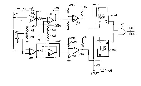
The present invention relates to a low
frequency discriminator circuit comprised if apparatus
for providing a rectangular wave input signal, apparatus
for integrating the input signal, apparatus for
detecting whether the integrated input signal falls
between upper and lower thresholds respectively, and
apparatus for providing an output signal indicating when
the integrated input signal falls between the
thresholds, whereby the frequency of the input signal
may be determined to be between higher and lower limits.


French Abstract

La présente invention est un circuit discriminateur basse fréquence constitué d'un circuit de génération de signaux en ondes rectangulaires, d'un circuit d'intégration de ces signaux, d'un circuit servant à détecter si les signaux intégrés se trouvent entre un seuil supérieur et un seuil inférieur, et d'un circuit produisant un signal indiquant quand le signal intégré se trouve entre les seuils mentionnés, ceci permettant alors d'établir que la fréquence du signal d'entrée du circuit intégrateur se trouve entre une limite supérieure et une limite inférieure.

Claims

Note: Claims are shown in the official language in which they were submitted.


I claim:
1. A low frequency discriminator circuit
comprising:
(a) means for providing a rectangular wave
input signal,
(b) means for integrating said input signal,
(c) means for detecting whether the integrated
input signal falls between upper and lower thresholds
respectively, and
(d) means for providing an output signal
indicating when the integrated input signal falls
between said thresholds,
whereby the frequency of the input signal may
be determined to be between higher and lower limits.
2. A discriminator circuit as defined in claim
1 in which said means for providing said input signal is
comprised of means for splitting an input signal into
two circuit paths, and wherein the integrating means is
comprised of means for integrating the input signal in
each of the circuit paths using different time constants
respectively relating to said higher and lower frequency
limits.
3. A discriminator as defined in claim 2 in
which said detecting means is comprised of a pair of
comparators, each set to a threshold, for receiving a
corresponding integrated input signal and for providing
an output signal of one or another polarity depending on
whether the corresponding integrated input signal is
above or below its threshold, said means for providing
an output signal being comprised of a pair of flip flops
each for receiving said output signal of one or another

logic level and for providing a TRUE or FALSE output
depending on said logic level input thereto.
4. A discriminator as defined in claim 3
further including an AND gate having one input connected
to a /Q output of one of the flip flops and another
input connected to a Q output of the other of the flip
flops.
5. A discriminator as defined in claim 4, in
which said limits of the input signal are approximately
23 - 54 Hz.
6. A discriminator as defined in claim 3
further including a buffer connected in each of the two
circuit paths for receiving the input signal and
delivering it to the integrators.
7. A discriminator as defined in claim 3, in
which each of the comparators includes a voltage divider
for setting the respective thresholds, the voltage
dividers being comprised of electronically controllable
potentiometers.
8. A discriminator as defined in claim 3, in
which the output signals of one or the other polarities
are applied to respective reset inputs of the flip
flops, and further including means for applying a
temporary set input signal to respective set inputs of
the flip flops prior to determining the outputs of the
flip flops.

9. A discriminator as defined in claim 8 in
which the set input signal is cyclical, timed to precede
the output signals of one or the other polarities being
applied to said reset inputs by an interval of time.
10. A discriminator as defined in claim 8 in
which the set input signal is a temporary low logic
level square wave pulse.
11. A discriminator as defined in claim 8, in
which each of the comparators includes a voltage divider
for setting the respective thresholds, the voltage
dividers being comprised of electronically controllable
potentiometers.
12. A discriminator as defined in claim 11
further including an AND gate having one input connected
to a /Q output of one of the flip flops and another
input connected to a Q output of the other of the flip
flops.
13. A discriminator as defined in claim 12
further including a buffer connected in each of the two
circuit paths for receiving the input signal and
delivering it to the integrators.
14. A discriminator as defined in claim 13, in
which said limits of the input signal are approximately
23 - 54 Hz.

Description

Note: Descriptions are shown in the official language in which they were submitted.


21238~7
FIELD OF THE INVENTION
This invention relates to the field of low
frequency discriminator circuits, and in particular to a
circuit that can discriminate low frequency telephone
ringing signals within a predetermined range.
BACKGROUND TO THE INVENTION
There are requirements from time to time to
discriminate between various frequency signals at the
low end of the frequency spectrum. One example of this
requirement is to have the capability of detecting
ringing signals in Germany over a narrow frequency band
of 23 Hz to 54 Hz. The same detector is also required
to not detect ringing signals that are at or below 18
Hz., or above 64 Hz. The detection is desired to result
in a logic signal that can be read by a microprocessor.
Attempts to achieve this type of requirement
have resulted in software programs which count timing
intervals of a rectangular wave generated by a portion
of a ringing detector circuit. This approach has worked
well in high speed microprocessor based systems and in
systems that have short intervals between interrupt
requests that use routines related to the interrupt
intervals when discriminating between low frequency
signals.
However, this approach has been found not to
work well in many slower microprocessor based systems,
or in systems which have relatively wide spacing between
interrupt requests when associated interrupt routines
are used for low frequency discrimination.
SUMMARY OF THE INVENTION
The present invention can discriminate between
low frequency signals, and provides a logic output which
can be read by slow microprocessor based systems. In
general, the input signal is integrated using two
different time constants each related to the boundaries

2l238~7
of the frequency range to be detected, the integrated
results respectively being tested against upper and
lower thresholds. The results of the tests is applied
to latches, preferably formed by flip flops, for
generation of logic signals that can be read by a
microprocessor.
In accordance with an embodiment of the
invention, a low frequency discriminator circuit is
comprised of apparatus for providing a rectangular wave
input signal, apparatus for integrating the input
signal. apparatus for detecting whether the integrated
input signal falls between upper and lower thresholds
respectively, and apparatus for providing an output
signal indicating when the integrated input signal falls
between the thresholds, whereby the frequency of the
input signal may be determined to be between higher and
lower limits.
In accordance with a preferred embodiment, in
the aforenoted circuit the apparatus for providing the
input signal is comprised of apparatus for splitting an
input signal into two circuit paths, and wherein the
integrating apparatus is comprised of apparatus for
integrating the input signal in each of the circuit
paths using different time constants respectively
relating to the higher and lower frequency limits.
In accordance with the preferred embodiment,
the detecting apparatus is comprised of a pair of
comparators, each set to a threshold, for receiving a
corresponding integrated input signal and for providing
an output signal of one or another polarity depending on
whether the corresponding integrated input signal is
above or below its threshold, the apparatus for
providing an output signal being comprised of a pair of
flip flops each for receiving the output signal of one

~ 1~38~
or another logic level and for providing a TRUE or FALSE
output depending on the logic level input thereto.
BRIEF INTRODUCTION TO THE DRAWINGS
A better underst~n~ing of the invention will be
obtained by reading the description of the invention
below, with reference to the following drawings, in
which:
Figure 1 is a schematic diagram of the
preferred embodiment of the invention, and
Figure 2 is a block diagram of an additional
aspect of an embodiment of the invention.
DETAILED DESCRIPTION OF A PREFERED EMBODIMENT
Turning Figure 1, an input signal is received
at input 3, where it is split into two paths, each
leading to the inverting input of an operational
amplifier 5A and SB. The noninverting inputs of
amplifiers 5A and 5B are connected together in a
conventional way to the tap of a voltage divider
comprised of series resistors 7A and 7B which are
connected between +5 V. and ground, bypassed with
capacitor 7C.
The outputs of amplifiers 5A and 5B are applied
to integrators 9A and 9B respectively, which are also
connected to the tap of a voltage divider comprised of
series resistors llA and llB, bypassed with capacitor
llC. The time constant of the integrators are
different, and establish different integration output
signal ramp slopes. For example, the time constant of
integrator 9A can be established by a resistor of 30K
ohms and a capacitor of 0.1 microfarad, while the time
constant of integrator 9B can be established by a
resistor of 75K ohms and a capacitor of 0.1 microfarad.
The outputs of the integrators are connected to
respective non-inverting inputs of comparators 13A and
13B. The inverting inputs of comparators 13A and 13B

~?/d 3~
are respectively connected to the taps of voltage
dividers comprised of series resistors l5A and 15B for
one comparator and series resistors 17A and 17B for the
other, which series resistors are connected between a
d.c.voltage source (e.g. +24 volts) and ground. In one
embodiment, the values of these resistors were chosen to
provide +3 . 85 volts at the inverting input of comparator
13A and +2 . 2 volts at the inverting input of comparator
13B .
Load resistors l9A and l9B connect the outputs
of the respective comparators 13A and 13B to a source of
voltage, e.g. +5 V.
The outputs of the comparators are connected to
the reset (R) inputs of respective flip flops 21A and
15 2 lB of a latch. In one embodiment the /Q and Q outputs
respectively of flip flops 2 lA and 2 lB are connected to
the inputs of an AND gate 2 3 .
In operation, the input signal is applied to
input 3, and must be rectangular in form, the timing of
which is dependent on the freguency of the signal to be
discriminated. If the signal to be detected is a sine
wave, it should be converted to a rectangular waveform
prior to application to this circuit.
The input signal is applied equally to
operational amplifiers 5A and 5B, where they are
buffered and inverted. Of course, if the input signal
is already split, buffered and in suitable form to be
integrated, the buffering and inverting stage may be
deleted.
The output signal from operational amplifiers
5A and 5B are applied to integrators 9A and 9B, which
integrate the rectangular waveshapes into ramps, having
different time constants. Thus for example the ramp
of a rectangular wave will rise slower when
A 4

2123847
integrated in integrator 9B than when integrated in
integrator 9A.
The outputs of the integrators are applied to
comparators 13A and 13B, where they are compared against
respective upper and lower thresholds. The thresholds
are set so that the comparators will trip to a low logic
level state when the input signals thereto fall below
their respective thresholds. Thus the output of
comparator 13A will go to low logic level when the input
frequency is below an upper threshold, and the output of
comparator 13B will go to low logic level when the input
frequency is below a lower threshold.
The outputs of comparators 13A and 13B are
input to the reset inputs to flip flops 21A and 21B, and
result in the following truth table at their outputs:
Test FF 2lA FF 2lB
Input (6OHz (2OHz
Freq thresh.) thresh.)
(Hz)
O 0
18 1 0
23
54
64 0
These output signals may be read through an
input/output port of a microprocessor to determine
whether a valid frequency in the range between the upper
and lower frequency thresholds have been detected.
However, to initiate a test for the occurrence of a
valid input frequency, the flip flops must be set. This
is obtained by applying a set input signal 23 to a start
input 25, which input is connected to the set (S) inputs
of flip flops 21A and 21B. The set input signal should

21238~7
be a temporary low logic rectangular wave of about 80
ms. Once set, the outputs of the flip flops should be
monitored for appropriate states as indicated by the
truth table example above.
To have the input frequency continuously
monitored, the set input signal can be applied at the
frequency of the input signal, and may be usefully
obtained from the microprocessor, or from another
circuit and derived from the input signal.
Instead of the microprocessor receiving the
logic states from the flip flops 21A and 21B and
deducing whether the frequency of the input signal is
within range, the /Q output of flip flop 2 lA and the Q
output of flip flop 21B may be applied to respective
inputs of AND gate 2 3 . The output of the AND gate
provides a TRUE logic signal if the input signal is
between the input thresholds. A microprocessor or other
circuit can thus distinguish whether the input signal
frequency is within or not within the range, by
monitoring the output logic level of the AND gate.
It should be noted that the frequencies of
different signals may be distinguished by appropriately
selecting the resistor and capacitor components of the
discriminator stages, and by appropriately selecting the
thresholds of the comparators. Electronically
controllable potentiometers may be used to select
frequency bands under control of a microprocessor.
A block diagram of such a selection system is
shown in Figure 2. A microprocessor 27 has control
outputs connected to electronically controlled
potentiometers 29 and 31. Potentiometers 29 and 31 are
representative of the voltage dividers formed of
resistors llA and llB, and representative alternatively
of voltage dividers formed of resistors 15A and 15B. Of
course it will be understood that two sets of voltage

21238~7
dividers may be controlled by the microprocessor, and as
well, the time constant setting capacitors and
resistors of integrators 9A and 9B may also be switched
and varied as required, by means of microprocessor 27.
In this manner the frequencies and bands to be
discriminated may be established under program control.
In addition, microprocessor 27 may also output
the set signal 25, either when it wishes to make a
frequency measurement, or on a cycling basis. In the
latter case it must monitor the actual input signal
frequency.
- A person understanding this invention may now
conceive of alternative structures and embodiments or
variations of the above. All of those which fall within
the scope of the claims appended hereto are considered
to be part of the present invention.

Representative Drawing
A single figure which represents the drawing illustrating the invention.
Administrative Status

2024-08-01:As part of the Next Generation Patents (NGP) transition, the Canadian Patents Database (CPD) now contains a more detailed Event History, which replicates the Event Log of our new back-office solution.

Please note that "Inactive:" events refers to events no longer in use in our new back-office solution.

For a clearer understanding of the status of the application/patent presented on this page, the site Disclaimer , as well as the definitions for Patent , Event History , Maintenance Fee  and Payment History  should be consulted.

Event History

Description Date
Inactive: Adhoc Request Documented 2018-06-06
Revocation of Agent Requirements Determined Compliant 2018-05-18
Appointment of Agent Requirements Determined Compliant 2018-05-18
Time Limit for Reversal Expired 2010-05-18
Letter Sent 2010-03-31
Letter Sent 2009-05-19
Letter Sent 2009-04-29
Letter Sent 2007-10-19
Inactive: IPC from MCD 2006-03-11
Letter Sent 2005-09-09
Letter Sent 2003-12-01
Inactive: Correspondence - Transfer 2003-09-29
Inactive: Office letter 2003-04-17
Grant by Issuance 1997-11-11
Inactive: Application prosecuted on TS as of Log entry date 1997-09-05
Inactive: Status info is complete as of Log entry date 1997-09-05
Pre-grant 1997-05-05
Notice of Allowance is Issued 1997-02-04
Application Published (Open to Public Inspection) 1995-09-12
Request for Examination Requirements Determined Compliant 1994-05-18
All Requirements for Examination Determined Compliant 1994-05-18

Abandonment History

There is no abandonment history.

Owners on Record

Note: Records showing the ownership history in alphabetical order.

Current Owners on Record
MITEL NETWORKS CORPORATION
Past Owners on Record
PATRICK H. CASSELMAN
Past Owners that do not appear in the "Owners on Record" listing will appear in other documentation within the application.
Documents

To view selected files, please enter reCAPTCHA code :


To view images, click a link in the Document Description column. To download the documents, select one or more checkboxes in the first column and then click the "Download Selected in PDF format (Zip Archive)" or the "Download Selected as Single PDF" button.

List of published and non-published patent-specific documents on the CPD .

If you have any difficulty accessing content, you can call the Client Service Centre at 1-866-997-1936 or send them an e-mail at CIPO Client Service Centre.


Document
Description 
Date
(yyyy-mm-dd) 
Number of pages   Size of Image (KB) 
Abstract 1995-09-11 1 15
Description 1995-09-11 7 279
Claims 1995-09-11 3 94
Drawings 1995-09-11 1 21
Description 1997-05-04 7 280
Representative drawing 1997-11-09 1 9
Maintenance Fee Notice 2009-06-29 1 171
Correspondence 2003-04-16 1 17
Fees 1998-04-29 1 46
Fees 1997-04-27 1 33
Fees 1996-04-16 1 31
Prosecution correspondence 1997-05-04 1 42
Prosecution correspondence 1997-05-04 1 22