Note: Descriptions are shown in the official language in which they were submitted.
CA 02123948 2004-04-20
77496-106
METHODS AND APPARATUS FOR THE MAKING OF ELECTRONIC ARTICLE
SURVEILLANCE TAGS AND IMPROVED ELECTRONIC ARTICLE
SURVEILLANCE TAGS PRODUCED THEREBY
FIELD OF THE INVENTION
This invention relates generally to electronic
article surveillance (EAS) and pertains more particularly to
providing improved methods and apparatus for the making of
EAS tags and improved tags resulting therefrom.
BACKGROUND OF THF~ INVENTION
The genesis of the subject invention resides in a
continuing effort to improve extant EAS tags (also called EAS
labels) and tag ~>roduction practices such as are set forth in
various commonly-assigned prior art patents, for example, U.S.
Patent No. 5,006,856 which issued April 9, 1991.
Tags of the '856 patent comprise spiral coils
disposed in generally facing relationship on opposed sides
of a dielectric layer, with the coils interconnected in an
area outside of the dielectric layer. A resonant circuit is
accordingly provided and is enclosed within electrically
insulative outer covering members.
In use, a tag is attached to an article to be
monitored as against fraudulent activity, and if the article
is carried to an exit of the surveillance zone, such as the
exit of a store, an alarm condition attends incidence of
energy on the tag of frequency equal to the resonant
frequency of the t:ag.
Tags having facility for "deactivation" are
likewise shown in the '856 patent and discussed also in
detail below. The deactivation structure may comprise an
electrically conductive
-1-
2123948
member astride the turns of one of the spiral coils and isolated
therefrom by an intervening layer of material which is normally
electrically insulative but, on incidence of high energy on the
tag, i.e., in excess of that required for causing alarming
resonance, converts to electrically conductive character. On that
event, the conductive member with the converted layer short-
circuits the spiral coil. The deactivation normally precludes the
tag from again resonating and typically takes place at a checkout
counter, from which the article with tag therewith can freely pass
from the surveillance zone.
As has been recognized in the past, electrostatic charge
buildup on individual tags can cause undesirable tag deactivation
by effecting conversion of the convertable layer. Such charge
buildup can occur in the course of tag production and further in
the course of printing on the tags. As is discussed also in detail
below, tags are produced in a continuous sequence, with the
deactivator structure applied continuously in the sequence, i.e.,
as a deactivator web providing electrical connection of the series
of tags in the course of being produced. While the continuous
deactivator web can function as a drain to prevent static discharge
from deactivating the labels during the manufacturing process, it
can also function as a vehicle for electrostatic charge to flow
across a sequence of tags causing deactivation of the tag sequence
in the course of production.
One past measure taken for avoiding such flow of electrostatic
charge has been to make cuts through the deactivator web, as in..
-2-
212~94~
Fig. 31 of the '856 patent (cuts 520). While the deactivator web
remains continuous between adjacent tags, the '856 patent notes the
cuts to be effective in preventing premature deactivation due to
electrostatic charge in the tag manufacturing equipment or
subsequently in printing equipment.
Another measure in this respect has been to provide a
conductive film for charge drain purposes, as is shown at 600, 601
in Fig. 31 of commonly-assigned prior art U.S. Patent No.
4 , 910 , 499 . The conductive film constitutes a component of the tags
following production and serves to drain charge also in the course
of printing. Its presence, however, prevents accurate
determination of the "Q'° of the tag. Further, the drain mechanism
is fully capacitive, given that an insulative web intervenes the
conductive film and the tag coil structure.
A further measure in this respect is seen in Figs. 25 and 26
of the '856 patent, where, at the completion of forming a sequence
of connected tags, holes 407 are punched through the deactivation
layer between adjacent tags to sever the same and render adjacent
tags with no electrical connection therebetween. This practice
affords electrical isolation of adjacent completed and connected
tags when they are collected on a reel. However, this measure
affords no relief as against electrostatic charge which may build
up in the preceding steps in the manufacture of the tags. Further,
since the holes are punched on completion of tag making, they
extend fully through all layers of the tag and are undesirably
viewable in the finished product.
-3-
212394
From applicant s viewpoint, the various past efforts to
overcome the adverse influence of electrostatic charge buildup
in/on deactivatable EAS tags/circuits, while constituting
meaningful steps in the evolution of correction of the problem and
providing effective production practice and effective tags, have
not yielded as low a reject rate in production as is optimally
desirable.
To provide more specific background discussion facilitating an
appreciation of the practices and tags of the subject invention,
detailed description of extant practices is now provided, with
reference to those drawings herein which are labelled as being
prior art.
Referring to Fig. 1, there is shown an exploded view of a tag
generally indicated at 19. The tag 19 is shown to include a sheet
20T having pressure sensitive adhesive 21 and 22 on opposite faces
thereof. A mask 23 in a spiral pattern covers a portion of the
adhesive 21 and a release sheet 24T is releasably adhered to the
adhesive 22. The mask 23 renders the adhesive 21 which it covers
non-tacky or substantially so.
A conductor spiral indicated generally at 25 includes a spiral
conductor 26 having a number_ of turns. The conductor 26 is of
substantially the same width throughout its length except for a
connector bar 27 at the outer end portion of the conductor spiral
26. There is a sheet of dielectric 28T over and adhered to the
conductor spiral 25 and the underlying sheet 20T by means of
adhesive 29. .
-4-
212398
A conductor spiral generally indicated at 30 includes a spiral
conductor 31 having a number of turns. The conductor 31 is adhered
to adhesive 29' on the dielectric 28T. The conductor 31 is
substantially the same width throughout its length except for a
connector bar 32 at the outer end portion of conductor spiral 30.
The conductor spirals 25 and 30 are generally aligned in face-
to-face relationship except for portions 33 which are not face-to-
face with the conductor 26 and except for portions 35 which are not
face-to-face with the conductor 31. A sheet 37T has a coating of
a pressure sensitive adhesive 38 masked off in a spiral pattern 39.
The exposed adhesive 38' is aligned with the conductor spiral 30.
Adhesive is shown in Fig. 1 by heavy stippling anc~.the masking is
shown in Fig. 1 by light stippling with cross-hatching.
The connector bars 27 and 32 are electrically connected, as
for example by staking 90 (Fig. 2). The staking 90 occurs where
connector bars 27 and 32 are separated only by adhesive 29 or are
in direct electrically conductive contact with no intervening
adhesive or other medium. There is no paper, film or the like
between the connector bars 27 and 32. Accordingly, the staking 90
is effective for electrically conductive interconnection of
connector bars 27 and 32.
The process for making the tag of Fig. 1, which does not
include deactivation structure, is described in Fig. 3 of the
°856 patent, to which patent incorporating reference is hereby
made for all purposes.
On the other hand, Fig. 3 herein shows that portion of the
-5-
z~~3~~s
'856 Fig. 3 manufacturing apparatus as modified to provide tags
with deactivation structure. A pair of coating and drying
stations is generally indicated at 111 and 112 where respective
coatings 113 and 114 in the form of continuous stripes are
printed and dried. The coating 113 is conductive and is applied
directly onto the pressure sensitive adhesive 38 on the web 37.
The coatings 114 are wider than the respective coatings 113
which they cover to assure electrical isolation, as best shown
in Figs. 4 and 5. The coatings 114 are composed of a normally
non-conductive activatable material.
Referring to Figs. 6 and 7, there is shown a finished
deactivatable tag 37T' with the coatings 113 and 114,, having been
severed as the tag 37T' is severed from the tag web as indicated
at 113T and 114T respectively. As shown the coating 113T is of
constant width and thickness throughout its length and the
coating 114T is of constant width and thickness but is wider
than the coating 113T. The coating 113T which is conductive is
thus electrically isolated from the conductor spiral 30. The
coatings 113T and 114T comprise an activatable connection A~
(Fig. 9) which can be activated by subjecting the tag to a high
level of energy above that for causing the resonant circuit to
be detected at an interrogation zone.
The showings of prior art practices in Figs. 8 and 9 herein
correspond to Figs. 24 and 25 of the '856 patent. The
deactivator webs 318 and 319, corresponding to the deactivator
structure 113T and 114T of Figs. 6 and 7 hereof, are separated
-6-
21239~~
into longitudinally spaced deactivator strips or stripes 318'
and 319'. The separation is accomplished in accordance with the
specific embodiment shown in Fig. 8, by punching out portions of
the web 238 and the deactivator webs 318 and 319 to provide
holes 407. For this purpose, a diagrammatically illustrated
rotary punch 403 and a rotary die 404 are used. The rotary punch
403 has punches 405 and the rotary die 404 has cooperating die
holes 406. The resultant holes 407 are narrower than the spacing
between the resonant circuits. The holes.407 are thus registered
with the margins of the longitudinally spaced resonant circuits
as shown in Fig. 9. Thus, the probability of arcing of static
electricity between resonant circuits in a Zongitudinal
direction and between deactivator strips 318' (or 319') is
lessened. However, such "severing" of the deactivation webs
takes place at a quite late stage in the manufacturing process
and does not preclude electrostatic charge movement in preceding
manufacturing process steps.
Figs. 10 and 11 herein correspond respectively with Figs.
31 and 32 of the '856 patent. In Fig. 10, resonant circuits RC
formed of connected pairs of spiral conductors 400 and 401
having plural turns are shown provided with an activatable
connection or deactivator AC. The deactivators AC are made from
a deactivator web ACW. In the manufacture of the tag web shown
in Fig. 10, the deactivator web ACW is cut as shown at 520.
Each cut 520 is more than a slit because it causes permanent
spacing or separation between portions or sections or strips
_7_
2123~~8
AC1, AC2 and AC3 associated with each tag T. As shown, each tag
T comprises the portion of the tag web between adjacent pairs of
phantom lines TL. The section AC1 extends between one end of the
tag T along one phantom line TL and a cut 520, the section AC2
extends between adjacent but spaced cuts 520 of a tag T, and the
section AC3 extends between the other cut 520 in the tag T and
the other end of the tag T along the other phantom line TL.
Such cutting or slitting is practiced at a quite early
stage of the manufacturing process since the deactivator web
must be exposed to perform the cutting.
Fig. 11 shows the upper spiral conductor 401. The
deactivator web ACW is comprised of normally non-conductive or
breakdown material 521. The deactivator web ACW is also
comprised of a deactivating conductor in the form of a vacuum
metalized coating 522 of aluminum to which the normally non-
conductive breakdown material 521 is adhered. The coating or
layer 522 is deposited on a polyester film 523 which acts as a
carrier or support for the coating 522 and the breakdown
material 521.
A mask pattern 524 (corresponding to mask pattern 23) is
disposed between the film 523 and an adhesive coating 525 on a
polyester film 526. The cuts 520 are identical and one of the
cuts 520 is shown in detail in Fig. 11. The cut 520 in Fig. 11
is shown to have two widths for a reason as will be evident from
Fig. 12.
The upper spiral conductor 401 has eight conductor
_g_
212398
portions 401-1 through 401-8 at first through eighth locations
numbered 1 through 8. In the preferred embodiment, one cut 520
is spaced between the first and second conductor portions 401-1
and 401-2, that is, between the first and second locations and
another cut 520 is spaced between the seventh and eighth
conductor portions 401-7 and 401-8 between the seventh and
eighth locations. The adjacent cuts 520 of any one tag
effectively make section AC2 the deactivator AC. It is evident
that the deactivator AC is adjacent and crosses less than all
the turns of the spiral conductor 401. When the deactivator AC
is operated, the breakdown coating 521 at one or more locations
2 through 7 becomes conductive and consequently the deactivating
conductor 522 becomes electrically connected to the resonant
circuit at the Location or locations 2 through 7 where breakdown
occurs. If there is breakdown at only one location, the
conductor 522 acts like a spur electrically connected to the
spiral conductor 401 and thus affects the resonant circuit.
However, breakdown can also occur at two or more locations,
second through seventh, which will electrically connect portions
of the spiral conductor 401 to each other to prevent detection
of the resonant circuit of the tag.
The. '856 patent states that there is even considerable
improvement in deactivation when a cut 520 is made through the
deactivator web ACW only between the first and second conductor
portions 401-1 and 401-2 or only between the seventh and eighth
conductor portions 401-7 and 401-8. In this case there is only
-g_
one cut 520 in the deactivator web in each tag. Accordingly, the
deactivator strip in each tag is separated into two deactivator
sections or deactivator strips.
The short deactivation strips, AC1 and AC3 across TL in
Fig. 10, however, provide electrical continuity between
successive circuits until the severing of the deactivator web
occurs, as noted at a quite late stage of the manufacturing
process.
Referring to Fig. 12, there is diagrammatically
illustrated a portion of the process for making the tags shown
in Figs. 10 and 11. Cutter roll 529 has cutter blades 530 which
produce the cuts 520 in the deactivator web ACW.~ The web 37
passes between the cutter roll 529 and a back-up roll 531. It
should be borne in mind that the web 37 is under tension as it
is drawn partially about rolls 67 and 116, heated drum 115 and
roll 117. The deactivator web has been cut into sections AC1,
AC2 and AC3, which are no longer in tension and therefore are
free to shrink. The deactivator sections AC1, AC2 and AC3 are
not under tension and consequently they do not stretch along
with the web 37. Specifically, with reference to Fig. 11, the
resulting cut opening 527 in the polyester film 526 the
associated adhesive 525 and pattern 524 are narrower than the
cut opening 528 in the deactivator AC and its associated
supporting or carrier web 523. Further, it is found that the
gap provided by cuts 520, clearly less than that afforded by
holes 407 (Fig. 9), is not of sufficient measure to effectively .
-10-
222348
insure preclusion of movement of electrostatic charge. Also,
the practices of cutting can themselves give rise to
electrostatic charge. Finally, it has been found that for the
cut tag version, higher deactivation field intensity is required
and that, with the tag retaining a partly non-deactivated coil,
i.e., that located outwardly of cuts 520, the deactivated tag
can, at times, still resonate as if it were not deactivated.
While the cuts 520 also have the effect of preventing
premature deactivation in the tag manufacturing equipment or
subsequently in printing equipment due to electrostatic charge,
applicant looks to the same, as in the case of the first
described approach to the electrostatic charge prpblem (holes
407 above) as not providing as low a reject rate in production
as is optimally desirable.
To summarize the state of the art, present practices call
for cutting the deactivator web at a quite early stage of the
process, since the deactivator web need be exposed for cutting.
This undermines the effectiveness of the deactivator web in any
subsequent static drain function. The continuous film drain
provided in dielectric coupling with the coil structures is
limited in that the charge drain is fully capacitive. Further,
in present practices, the severing of the deactivator web takes
place at a final stage of the process, and such step thus does
not afford benefit in electrically separating adjacent tags
during manufacture up to such final stage. Also, the step
provides a hole extending fully through the tag which, to
-11-
212394
certain users, is aesthetically undesired.
SUMMARY OF THE INVENTION
The present invention has as its principal object the
provision of improved methods and apparatus for deactivatable
EAS tag manufacture.
A particular object of the invention is to more effectively
address the electrostatic charge problem in present
deactivatable tag making methods.
A further object of the invention is to provide
deactivatable tags which exhibit electrical and mechanical
integrity enhanced over that of the above-disg"ussed prior
deactivatable tags.
In overall perspective, applicant has devised a practice by
which severing of the deactivator web can take place at an early
stage of the manufacturing process and yet continuous, enhanced
electrostatic charge drain is enabled throughout the
manufacturing process.
To these ends, the invention provides, in one aspect
thereof, an improvement in a method for the manufacture of
electronic surveillance tags by providing a continuous web of
electrically insulative material, applying to opposed surfaces
of the electrically insulative material web a succession of
first and second electrically conductive coils and applying to
the succession of first electrically conductive coils a normally
electrically insulative deactivation structure extending across
-12-
2123948
the first coil succession and convertible to be electrically
conductive, the improvement comprising the step of providing an
electrostatic charge drain in electrically conductive relation
with each of the first electrically conductive coils
substantially throughout the manufacture of the tags. The new
step may be practiced by providing an electrically grounded,
elongate, electrically conductive member across the succession
of first electrically conductive coils in electrical continuity
therewith. Alternatively, the step may be practiced by
configuring the succession of first coils integrally with the
electrostatic charge drain and electrically grounding the drain.
In either case, the drain is removed in a final Stage of tag
manufacture and does not interfere with accurate measurement of
the Q of the tags.
Based on continuous drainage of electrostatic charge during
most of the manufacturing process, the invention affords, in a
second aspect, the flexibility of selecting the point for
rendering the deactivator structure separate as between
successive coils to which it is applied. Thus, arty
electrostatic charge buildup on the deactivator structure giving
rise to deactivation of an individual tag is likewise bled to
ground, since such event provides electrical continuity with the
underlying coil and with the drain. The deactivation is
accordingly limited to such individual tag.
In a third aspect, the invention provides an improvement to
a method for the manufacture of electronic surveillance tags by
-13-
CA 02123948 2004-04-20
77496-106
providing a web of electrically insulative material,
applying to opposed surfaces of the electrically insulative
material web a succession of first and second electrically
conductive coils and applying to the succession of first
electrically conductive coils a normally electrically
insulative deactivation structure extending across the firsi~
coil succession ~~nd convertible to be electrically
conductive, the .improvement comprising the step of removing
the deactivation structure between the first electrically
conductive coils without disturbance to the coils and
without removal of the supporting insulative web or its
adhesive layer. The removing step is practiced in such
manner that the completed tag does not evidence any hole
therethrough and exhibits continuous exterior surfaces.
The rernoving step is preferably practiced by
cutting the deactivation structure exclusively transversely
of the succession of first electrically conductive coils anc.
vacuum withdrawing the cut portion of the deactivation
structure. The step is further practiced at an early stage
of the process, i..e., at a point in time prior to
application of the first and second coil successions to
opposite sides of the dielectric web.
Tags anal tag successions so produced constitute
further aspects of the invention, as does the apparatus
effecting the cutting and removal step.
A broad aspect of the invention provides in a
method for the manufacture of deactivatable electronic
article surveillance tags by providing a continuous web of
electrically insulative material, applying to opposed
surfaces of said electrically insulative material web a
succession of first and second electrically conductive coils
and applying to said succession of first electrically
-14-
CA 02123948 2004-04-20
77496-106
conductive coils a normally electrically insulative
deactivation structure extending across the first coil
succession and convertible to be electrically conductive,
the improvement comprising providing an electrically
grounded electrostatic charge drain in electrically
conductive relation with each of said first electrically
conductive coils substantially throughout the manufacture of:
said tags and removing said electrostatic charge drain from
said tags in a final stage of manufacture thereof.
A broad aspect of the invention provides in a
method for the manufacture of electronic article
surveillance tags by providing a continuous web of
electrically insulative material, applying to opposed
surfaces of said electrically insulative material web a
succession of first and second electrically conductive coils
and applying to said succession of first electrically
conductive coils a continuous deactivator web extending
across the first coil succession, the improvement comprising
draining electrostatic charge electrically conductively to
ground from each of said first electrically conductive coils
up to a final stage in the manufacture of said tags at which
stage said first and second successions of coils are in
facing relation across said web of electrically insulative
material and rendering the deactivator web discontinuous
between successive= of said first electrically conductive
coils at a prior manufacturing stage, said draining of
electrostatic charge conductively to ground from each of
said first electrically conductive coils being practiced by
laminating an electrostatic drain web to said insulative
material web and wherein said electrostatic charge drain web
is selected to be of dimension substantially lesser than the
transverse expanse of said insulative material web, said
electrostatic charge drain web being configured as a
-14a-
CA 02123948 2004-04-20
77496-106
marginal portion of said succession of said first
electrically conductive coils.
A broad aspect of the invention provides in a
method for the manufacture of electronic article
surveillance tags by providing a continuous web of
electrically insulative material, applying to opposed
surfaces of said electrically insulative material web a
succession of first and second electrically conductive coils
and applying to said succession of first electrically
conductive coils a continuous web of normally electrically
insulative deactivation structure extending across the first
coil succession and convertible to be electrically
conductive, the improvement comprising rendering said
deactivation structure web discontinuous by removing
portions thereof without attendant removal of portions of
said web of electrically insulative material in registry
with said removed deactivation structure web portions, said
removing of portions of said deactivation structure web
being practiced by making transverse cuts therethrough
lengthwise in excess of a transverse dimension of said
deactivation structure web, said cuts not extending
longitudinally of said deactivation structure web, said cuts
extend also into but not through said web of electrically
insulative material.
A broad aspect of the invention provides in a
method for the manufacture of electronic article
surveillance tags by providing a continuous web of
electrically insulative material, applying to opposed
surfaces of said electrically insulative material web a
succession of first and second electrically conductive coils
and applying to said succession of first electrically
conductive coils a continuous web of normally electrically
-14b-
CA 02123948 2004-04-20
77496-106
insulative deactivation structure extending across the first
coil succession and convertible to be electrically
conductive, the improvement comprising draining
electrostatic charge electrically conductively to ground
from each of said first electrically conductive coils up to
a given stage in the manufacture of said tags at which stage
said first and second successions of coils are in facing
relation across said web of electrically insulative material.
and rendering said deactivation structure web discontinuous
at a manufacturing stage preceding said given stage, said
rendering of saia. deactivation structure web discontinuous
being practiced by removing portions thereof without
attending removal of portions of said web of electrically
insulative material in registry with said removed
deactivation structure web portions by making transverse
cuts therethrough lengthwise in a transverse dimension of
said deactivation structure web, said cuts not extending
longitudinally of said deactivation structure web, said cuts
extend also into but not through said web of electrically
insulative material.
A broad aspect of the invention provides in a
method for the manufacture of electronic article
surveillance tags by providing a continuous web of
electrically insulative material, applying to opposed
surfaces of said electrically insulative material web a
succession of first and second electrically conductive coils
and applying to said succession of first electrically
conductive coils a normally electrically insulative
deactivator web ext=ending across the first coil succession,
the improvement whe rein said deactivator web is rendered
discontinuous between said first electrically conductive
coils prior to said step of applying said succession of
first and second electrically conductive coils to opposed
-14c-
CA 02123948 2004-04-20
77496-106
surfaces of said electrically insulative material web,
providing an electrostatic charge drain to ground
electrically conductively for each of said first
electrically conductive coils following application thereof
to said web, and the further step of removing said
electrostatic charge drain from said tags in a final stage
of manufacture thereof.
The foregoing and other objects and features of
the invention will be understood from the following detailed
description of the invention and from the drawings wherein
like
-14d-
212398
reference numerals identify like components throughout.
DESCRIPTION OF THE DRAWINGS
Fig. 1 is an exploded perspective view of a tag produced by
extant tag making methods.
Fig. 2 is a fragmentary cross-sectional view of the Fig. 1
tag.
Fig. 3 is a fragmentary perspective view which illustrates
apparatus of an extant method of making deactivatable tags.
Fig. 4 is a fragmentary top plan view taken along line 4--4
of Fig. 3.
Fig. 5 is a sectional view taken along line 5-t5 of Fig. 4.
Fig. 6 is a fragmentary perspective view similar to Fig. 1,
but showing one embodiment of structure for deactivating the
tag.
Fig. 7 is a fragmentary top plan view of the tag shown in
Fig. 6.
Fag. 8 is a fragmentary perspective view which illustrates
apparatus of an extant deactivatable tag making method having
lessened susceptibility to electrostatic charge.
Fig. 9 is a fragmentary top plan view of a succession of
tags made in accordance with the Fig. 8 method.
Fig. 10 is a fragmentary top plan view of a succession of
tags made in accordance with an alternative extant deactivatable
tag making method having lessened susceptibility to
electrostatic charge.
-15-
212394
Fig. 11 is a fragmentary sectional view as would be seen
from plane 11-11 of Fig. 10.
Fig. 12 is a fragmentary perspective view which illustrates
apparatus of the extant alternative deactivatable tag making
method.
Fig. 13 is a fragmentary perspective view which illustrates
apparatus of a deactivatable tag making method having lessened
susceptibility to electrostatic charge in accordance with the
present invention.
Fig. 14 is a perspective view of cutting and removing
apparatus of the invention for removing deactivation structure
between successive coils.
Fig. 15 is a perspective view of a cutting unit of the Fig.
14 apparatus.
Fig. 16 is a sectional view of the Fig. 15 cutting unit.
Fig. 17 is a schematic view descriptive of a situation
prior to practice of the deactivator web removal step.
Fig. 18 is a schematic view descriptive of the situation
following practice of the deactivator web removal step.
Fig. 19 a plan view of an alternative embodiment of coil
structure in accordance with the invention.
DETAILED DESCRIPTION OF PREFERRED EMBODIMENTS AND PRACTICES
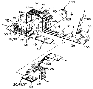
Referring to Fig. 13, roll 54 is shown to be comprised of
a composite web 55 having a web 20 with a full-gum or continuous
coating of pressure sensitive adhesive 38 and a release liner or
-16-
~~2399:8
web 56 releasably adhered to the upper side of the web 37 by the
pressure sensitive adhesive 38. As shown, the release liner 56 .
is delaminated from the web 37 to expose the adhesive 38. The
adhesive coated web passes under a pair of coating and drying
stations indicated at 111 and 112 and partially around a sand
paper coated roll 57.
While the above described practice is that of the method of
Fig. 3 of the '856, applicant departs therefrom at this juncture
by introducing a narrow web 601 of planar, electrically
conductive material such as copper or aluminum from a roll 600.
Web 601 is laminated onto the coated web 37 as it passes
partially around sandpaper roll 57.
Return is now to the practice per the '856 patent wherein
the composite web 37 passes partially around rollers 59 and 61,
through dryer 62, and partially around roller 63 where it meets
web 20, 49. Webs 20, 49, 37 pass partially around rollers 65 and
66 and delaminate at roller 66.
As is discussed in the '856 patent, the coil patterns are
electrically connected transversely. Further, they are Ln
electrical connection with web 601. Accordingly with web 601
electrically grounded, throughout the process, until such time
as web 601 is removed, electrostatic charge is drained as it
occurs. Thus, the above-discussed deactivation of tags in the
course of manufacture arising from their interconnection
sequentially by the applied deactivation structure through
electrostatic charge buildup and travel thereof is precluded per
-17-
212394
this aspect of the subject invention.
Whereas the punching operation, i.e., full separation of
the deactivator structure of the extant practice in Fig. 9
occurs late in the process, the present invention, by reason of
the presence of the electrostatic charge drain substantially
throughout the process, affords the opportunity to place the
deactivation structure removal step earlier in the sequence of
operations. The cutting practice of the extant practice shown
in Fig. 10 can now be omitted. Thus, the new practice of Fig.
14 is the only step needed with respect to removal of
deactivation structure.
Referring to Fig. 14, composite web 37 is advanced over
anvil roll 605. Vacuum cutting apparatus, generally shown at
606, includes roll 607 which has bearers 608 and 609 at ends
thereof. Vacuum ports are shown at 610 and 611. Roll 607 has
a hollow interior in communication with a vacuum source (not
shown) through ports 610 and 611. Roll 605 and roll 607 replace
roll 531 and roll 529 respectively of Figure 12 as well as as
well as roll 403 and 404 of Fig. 9. Cuts made by blades 614 and
615 do not penetrate through web 37 and would not be visible as
shown at 520 in Figure 12 or 407 in Fig. 9.
Roll 607 has insert pockets in which are disposed cutting
units 612. The structure of the cutting units is best seen in
Figs. 15 and 16, which show one cutting unit respectively in
perspective and in cross-section. Cutting unit 612 is comprised
of a metal body having an opening 613 in its upper surface and
-18-
21~394~
having a passage 613a extending fully therethrough into flow
communication with the hollow interior of roll 607. Cutting
blades 614 and 615 are located in bounding relation with the
opening 613, but, of consequence discussed below, are not
continuous perimetrically with opening 613,'i.e., the ends of
opening 613 are open to the ambient environment when the cutting
blades are in cutting relation with web 37.
Referring again to Fig. 14, composite web 37 bears the
opposed first and successions of coils and deactivator web 616
applied to one of the coil successions. The deactivator web is
removed at locations 617, i.e., the deactivator web portion (ACW
above) which intervenes successive coils, by action of cutting
units 612 as now discussed.
Evidently, the spacing of cutting units perimetrically of
roll 607 is equal to the length linewise between the deactivator
portions desired to be removed as composite web 37 seats on
anvil roll 605. If it were desired to cut fully through
composite web 37, the height of the cutting blades would be made
equal to the extent of bearers 608 arid 609 radially outwardly pf
roll 607, or vice versa. On the other hand, per the subject
invention, the height of the cutting blades 614 and 615 is
selected to be shorter than the extent of bearers 608 and 609
radially outwardly of roll 607, or vice versa, i.e., such that
the depthwise amount of material removed from composite web 37
is less than the depth of the web.
Referring to Fig. 17, it depicts a portion of composite web
-19-
_, 21~3~~8
37, showing two resonant tags 618 and 619 prior to the cutting
thereof. Each tag has an Outer insulative layer 620, a deadener
layer 623, a deactivator layer 621 (comprised by web 616 of Fig.
14), and a coil layer 622, bridged by the deactivator layer 621.
The results of the cutting operation are shown in Fig. 18.
As illustrated, a plug of material 624, inclusive only of
material previously of layer 621, is removed from web 616 by the
action of the Fig. 14 apparatus. For such purpose, the desired
cutting depth 625 of Fig. 17 is realized by making the
difference between the extent of bearers 608 and 609 radially
outwardly of roll 607 and the height of cutting blades equal to
the measure of depth 625.
Of significance to applicant's above interrelating of the
cutting blades, the bearers and the composite web dimensional
characteristics is that coil layer 622 is fully uninvaded or
mechanically disturbed. The deactivator portion is removed with
little, if any invasion of outer insulative 620. Further, the
vacuuming activity is limited to plug 624 which limits the
amount of removal of adhesive, rendering the vacuum removal
simpler and limiting need for manufacturing line interruption to
clean the vacuum apparatus. In this aspect, the subject
invention overcomes the disadvantages attending the extant
practice above discussed in connection with Fig. 9, wherein
holes 407 are punched fully through the resonant circuits,
giving rise to invasion of all layers and need for removal of
adhesives therein.
-20-
21~~948
The tag succession in Fig. 18 is a novel article reached in
the course of manufacture of deactivatable EAS tags,
constituting a tag succession in which a continuous, i.e.,
unperforated, outer web 620 bounding an interior deactivator web
having discontinuities between adjacent tags in the succession.
Further, individual, i.e., separated, tags which result from the
use of such article reached in the course of manufacture are
likewise novel in having continuous bounding surfaces with
deactivation structure therein which is recessed from a margin
of the tag. Thus, as is seen in Figs. 17 and 18, the line of
separation LS for adjacent tag parts 618 and 619 extends beyond
the end of deactivator layer 621 following removal of portion
624 thereof. Otherwise viewed, the individual tags so produced
define unperforated bounding surfaces with an interior void
adjacent the deactivation structure thereof.
Returning to discussion of the consequence of maintaining
cutting blades 613 and 614 discontinuous, i.e., open at their
respective ends to the ambient environment, any extent of
cutting into outer insulative layer 620 causes only
discontinuous side cuts, rather than full perimetric cuts,
resulting in the outer insulative layer remaining wholly intact.
Further, the open-ended cutting blade configuration enhances
vacuum removal efficiency.
While the embodiment of Fig. 13 above involved the use of
an electrostatic drain which was separate from the metal web
forming the coils, the invention contemplates the converse
-21-
2123943
situation, i.e., wherein the electrostatic drain is integral
with the metal web. Referring to Fig. 19, which corresponds in
part to Fig. 22 of the 'S56 patent, the metal web, which may be
comprised of copper or aluminum, is of increased transverse
dimension, encompassing conductive strip CS at one margin
thereof. Coils 401 are the coils to which the deactivator
structure is to be applied. Conductive strip CS is formed
integrally with the coils and thus has electrical connection to
coils 401. It remains in place, electrically grounded, until a
final phase of the manufacturing process, providing
electrostatic charge drain and permitting flexibility in
selection of the point in the process of removal of the
deactivator portions. At the final phase, conductive strip CS
is cut from the coil structures along cutting line CL of Fig.
19:
In summary of the foregoing and by way of introduction to
the ensuing claims, one method of the invention provides for the
manufacture of deactivatable electronic article surveillance
tags by providing a continuous web of electrically insulative
material, applying to opposed surfaces of the electrically
insulative material web a succession of first and second
electrically conductive coils and applying to the succession of
first electrically conductive coils a normally electrically
insulative deactivation structure extending across the first
coil succession and convertible to be electrically conductive,
the improvement comprising the step of providing an
-22-
212~9~8
electrostatic charge drain in electrically conductive relation
with each of the first electrically conductive coils
substantially throughout the manufacture of the tags.
The step of providing an electrostatic charge drain is
practiced by providing an elongate electrically conductive
member across the succession of first electrically conductive
coils in electrical continuity therewith, the elongate
electrically conductive member and the deactivation structure
being disposed on a common side of the succession of first
electrically conductive coils in mutually spaced relation
transversely thereof. Preferably, the elongate electrically
conductive member is disposed along a transverse margin of the
succession of first electrically conductive coils and the
deactivation structure is disposed generally centrally of the
succession of first electrically conductive coils.
The method includes the further step of removing a portion
of the deactivator structure from the tags in an early stage of
manufacture and removing the electrostatic charge drain from the
tags in a final stage of manufacture thereof. ,
The succession of first electrically conductive coils is
provided by the use of a continuous web of electrically
conductive material cut to form the succession of first
electrically conductive coils and the electrostatic charge drain
may be formed also from the continuous web of electrically
conductive material. In this case, the step of removing the
electrostatic charge drain by cutting the same from the
-23-
212394
succession of first electrically conductive coils in a final
stage of manufacture of the tags.
The insulative material web is preferably provided with a
continuous electrostatic charge drain web comprised of
electrically conductive material prior to application of the
succession of first electrically conductive coils to the
insulative material web and disposing the succession of first
electrically conductive coils in contact with the continuous
electrostatic charge drain web.
A further method of the invention effects the manufacture
of electronic article surveillance tags by providing a
continuous web of electrically insulative material,.applying to
opposed surfaces of the electrically insulative material web a
succession of first and second electrically conductive coils and
applying to the succession of first electrically conductive
coils a continuous deactivator web extending across the first
coil succession, the improvement comprising the steps of
draining electrostatic charge from each of the first
electrically conductive coils up to a final stage in the
manufacture of the tags at which stage the first and second
successions of coils are in facing relation across the web of
electrically insulative material and rendering the deactivation
structure web discontinuous between successive of said first
electrically conductive coils at a prior manufacturing stage.
The step of rendering the deactivator web discontinuous is
practiced by removing portions thereof without attendant removal
-24-
2123948
of portions of the web of electrically insulative material in
registry with the removed deactivator web portions. In
particular, the removal step is practiced by making transverse
cuts lengthwise in excess of a transverse dimension of the
deactivator web, the cuts not extending longitudinally of the
deactivator web. The cuts may extend also into but not through
the web of electrically insulative material. The removing step
is practiced by vacuum apparatus.
The structure depicted in Fig 18, will be seen to
constitute a new deactivatable EAS tag structure obtained in the
course of manufacture of electronic article surveillance tags.
Thus the illustrated structure comprises a succession of
mutually spaced conductive circuits on an insulative layer with
a deactivation structure placed between the conductive circuits
and the insulative layer, the deactivation structure being
discontinuous between conductive circuits in the succession, and
the insulative layer being continuous between conductive
circuits in the succession. Also, as above noted, individual
deactivatable EAS tags per the invention, exhibit novel
structure.
Apparatus for use in vacuum removal of a selected layer
from a multilayered web structure is also at hand, comprising a
cutting roll having a hollow interior and at least one vacuum
port communicating with the interior for connection to a vacuum
source, the cutting roll supporting a pair of perimetrically
spaced cutting blades directed longitudinally of the cutting
-25-
2123948
roll on an exterior surface thereof and defining a passage
extending from open space between the cutting blades into the .
hollow interior thereof. The apparatus further includes bearers
supported on the cutting roll to rotate therewith and an anvil
roll disposed in contact with the bearers. The extent of the
cutting blades radially exteriorly of the cutting roll and the
radial distance between the bearers and the cutting roll are of
respective measures effecting the selective layer removal.
Various changes in practice and modifications in
structure may evidently be introduced in the foregoing
particularly disclosed and described embodiments and practices
without departing from the invention. Thus, such. embodiments
and practices are intended in an illustrative and not in a
limiting sense. The true spirit and scope of the invention is
set forth in the ensuing claims.
-26-