Note: Descriptions are shown in the official language in which they were submitted.
METHOD AND APPARATUS TO PERFORM DIGITAL DEMODULATION
FIELD O~ THE INVENTION
This invention relates to a method and apparatus for
detecting and demodulating signals with temporally modulated
features, and particularly to frequency modulated signals
BACKGROUND OF THE INVENTION
In Frequency Modulation (FM), a sinusoidal carrier
signal of constant amplitude and frequency is modulated by
an input signal of a lower frequency and of varying
amplitude. FM thereby produces an output signal that is
constant in amplitude, varying in frequency in accordance
with the input signal, and within a specified frequency range
called the deviation bandwidth. In particular, the
instantaneous amplitude of the input signal is linearly
transformed into a change dw in the instantaneous frequency
~(t) of the carrier frequency ~c- To recover the input
modulating signal from the output modulation signal,
frequency demodulation must be performed using an FM
demodulator.
FM demodulators are well known, and consist of devices
such as ratio detectors, Foster Seeley discriminators, phase-
locked loop detectors, pulse-counting detectors, and
quadrature or coincidence detectors. All- of these
demodulators -- whether implemented as analog or digital
~'
WO93/10596 PCT/US92/098~-
2 1 ~
-- 2
apparatus -- pass data to post-processing stages, and
ultimately to an output amplifier.
For example, the Heathkit AJ-1510 Digital FM Tuner
employs a digital discrimination technique for demodulating
a frequency modulated signal. The discriminator is of the
pulse position modulation type, is inductorless and
diodeless, and contains two integrated circuits: a
retriggerable monostable multivibrator, and an operational
amplifier. An input signal at the retriggerable monostable
multivibrator causes it to change states for a fixed period
of time, as determined by an RC network to provide a sequence
of pulses of constant width and amplitude that are generated
at about one-half of the IF rate. Each pulse represents a
zero-crossing event. Signal information is represented as
deviations in the frequency of the zero-crossing pulses from
a constant IF frequency.
In a pulse integration type of FM demodulator, the
frequency modulated signals typically are amplified and
"hard-limited" to produce square waves which have zero-
crossings spaced in the same manner as the zero-crossings of
the FM signals. The square waves are then converted into a
sequence of constant width and amplitude pulses, one pulse
for each zero-crossing of the modulated input signal. Each
pulse is integrated (or filtered) and subsequently
differentiated to reproduce the modulating input signal
information.
There are pulse integration demodulators that employ a
single one-shot multivibrator that is triggered at each zero-
crossing. However, recovery time difficulties are
encountered during high frequency operation because the
internal delay of the multivibrator approaches the period of
the high frequency signals as the operating frequency is
increased.
In another form of pulse integration demodulator, a
source of frequency modulated signals is coupled to a
coincidence detector by a first and second signal path. The
W~93/10596 ~1 2 ~ PCT/US92/098~7
-- 3
first and second signal paths have unequal signal delay
characteristics, so that the coincidence detector provides
an output signal that includes a series of constant width
pulses, wherein pulse width is determined by a difference in
signal delay between the first and second signal paths. A
low pass filter is coupled to the coincidence detector to
recover the signal modulation represented by the series of
constant width pulses. However, this form of pulse
integrator exhibits operating disadvantages due to
non-linearity of the integrating network which impairs its
ability to perform sufficiently precise integration on the
applied signal pulse train.
SUMMARY OF THE INVENTION
An apparatus and method is provided for demodulating a
frequency modulated (FM), pulse-width modulated (PWM), or
other temporally modulated signal. Without employing an
analog-to-digital converter, modulating signal information
is extracted from a modulated signal as numerical
information. To demodulate an FM signal, for example, a high
gain stage is applied to an incoming FM signal to produce a
corresponding sequence of square waves. The period between
zero-crossings of the square waves is precisely measured and
represented numerically using a high-speed clock and at least
one counter. Numerical period information is then provided
to a signal processor that serves to convert the sequence of
period measurement values into a demodulated signal with a
high signal-to-noise ratio.
After a received FM signal is heterodyned with a local
oscillator signal, the resulting FM intermediate frequency
(IF) signal is "hard-limited" to yield a hard-limited FM IF
signal that substantially resembles a sequence of square
waves which are provided to a sign detector for detecting
zero-crossings. In preferred embodiments, the frequency of
- the local oscillator signal is chosen so as to yield
relatively low FM IF fre~uencies. The sign detector is
W093/10596 PCT/US92/09857
coupled to a pair of gating circuits, each gating circuit
being coupled to a respective pulse counter, and to a clock.
The gating circuits are alternately enabled in accordance
with the instantaneous sign of the hard-limited FM IF signal.
When enabled, each sample gating circuit provides a sequence
of clock pulses from the clock to a respective pulse counter.
Each pulse counter stores a respective count value that
represents the period between zero-crossings of the hard-
limited FM IF signal. The foregoing elements together
constitute a digital discriminator. In one embodiment, a
numerical processor, connected to the counters of the digital
discriminator, is responsive to the changing respective count
values, and reconstructs in real time the original modulating
input signal. The numerical processor performs calculations
upon the signal including: weighting, scaling, impulse
response filtering, windowing, and interpolationjdecimation.
Increasing the rate of the clock yields improved resolution
in the reconstructed modulating signal, up to the maximum
resolution of the counting circuit. Subsequent digital
filtering provides a low pass filter function that
effectively eliminates high frequency components.
The digital demodulator of the invention exploits the
linearity of digital processing to provide excellent
performance. Since the demodulation method of the invention
requires only low level signals and introduces minimal noise,
lower total noise levels result, and a high signal-to-noise
ratio is achieved. Consequently, the demodulator of the
invention can more easily receive weak signals, and suffers
fewer "drop-outs", a problem that is now common in fringe
reception areas, as well as in dense urban centers. Also,
the invention reduces the need for amplification of a
received signal, thereby increasing reliability and reception
quality. Therefore, at a given level of transmission power,
greater transmission range is possible. One potential
product area is in satellite broadcast applications; a
smaller antenna could be used when the method of the
WO93/10~96 r~ L 1~ PCT/US92/098~/
.~_
-- 5 --
invention is employed within the receiver. Further, the
invention can be practiced using currently available,
relatively inexpensive components. Also, since it is
consistent and cooperative with existing modulation standards
and transmission formats, the invention actually increases
the value of the currently installed base of transmission
equipment. Although the invention provides benefits when
included in 2-way radio, cellular telephone, and FM broadcast
applications, the invention is not limited to a specific
frequency band, or to a particular application.
The demodulation method and apparatus of the invention
introduces negligible noise, as contrasted with the levels
of noise added by conventional FM demodulation circuitry.
In another embodiment of the invention, a so-termed
"reciprocal fit count scaling" method is employed that
provides better performance than a linear count scaling
method, and improved performance with respect to a least-
squares-fit, nonlinear count scaling method. Such improved
performance provides an estimated signal with significantly
higher scaling accuracy, lower total harmonic distortion, and
an excellent signal-to-noise ratio. In fact, the reciprocal
count scaling method provides an exact analytic solution, and
guarantees the most accurate and optimal results attainable
from a system of this type.
DESCRIPTION OF THE DRAWING
The invention will be more fully understood from the
following detailed description, in conjunction with the
accompanying figures, in which:
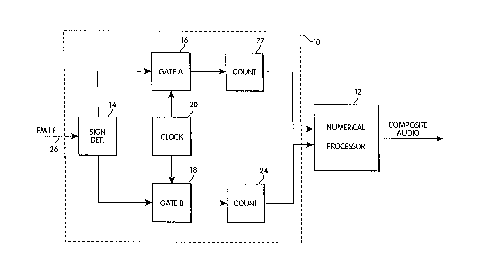
Fig. 1 is a block diagram of a digital discriminator
cooperative with a numerical processor;
Fig. lA is a block diagram of a digital discri ~nator
cooperative with a signal processor;
Fig. lB is a ~lock diagram of a digital discriminator
cooperative with a digital to analog converter;
WO93/10596 PCT/US92/098~7
]
-- 6
Fig. 2 is a schematic diagram of a digital discriminator
of the type which may be used in the circuits of Figs. 1, lA
and lB;
Fig. 3 is a flow diagram of a process implemented by the
numerical processor of Fig. 1;
Fig. 3A is a flow diagram of a process that includes
reciprocal fit count scaling;
Fig. 3B is a flow diagram of a process that includes
reciprocal fit count scaling and window functions;
Fig. 3C is a flow diagram of a process that includes a
bounds-checking routine and a second order fit;
Fig. 4 is a plot of linear scaled and weighted count
values versus the original count values, together with a plot
of scaled and weighted count values augmented with a
second-order nonlinear term versus the original count values;
Fig. 5 is a plot of the difference of the linear scaled
and weighted count values and the scaled and weighted count
values augmented with a second-order nonlinear term, versus
the original count values;
Fig. 6 is a plot of scaled and weighted count values
augmented with a second-order nonlinear term versus the
original count values, together with a plot of reciprocal fit
count values versus the original count values; and
Fig. 7 is a plot of the difference of the scaled and
weighted count values augmented with a second-order nonlinear
term and the reciprocal fit count values, versus the original
count values.
DESCRIPTION OF THE PREFERRED EMBODIMENT
With reference to Fig. 1, a digital discriminator 10 is
shown in cooperation with a numerical processor 12. The
digital discriminator 10 utilizes zero-crossing detection and
period measurement of a "hard-limited" FM IF signal to
recover an associated modulating signal by exploiting the
fact that the instantaneous frequency of an FM IF signal is
CA 02124114 1998-11-2~
inversely proportional to the instantaneous period of the
associated modulating signal.
Discrimination is accomplished by applying a "hard-
limited" FM IF signal to the sign detector 14. To form a
hard-limited signal, an input signal is amplified and then
clipped to provide what is essentially a square wave. The
sign detector 14 ascertains the instantaneous polarity along
each corresponding half-cycle of the FM IF signal, thereby
defining the moment of each zero-crossing. The period
between zero-crossings is determined by providing information
regarding the moment of each zero-crossing to gating circuits
16 and 18. The gating circuits 16 and 18 are alternately
enabled or disabled in accordance with the instantaneous sign
of the hard-limited FM IF signal provided by the sign
detector 14. When enabled, each sample gating circuit
provides a sequence of clock pulses from the clock 20 to a
respective pulse counter 22 or 24 until the other sample
gating circuitry 18 or 16 is enabled. A short sequence of
clock pulses between zero-crossings corresponds to a large
modulating signal amplitude, while a long sequence of system
clock pulses corresponds to a small modulating signal
amplitude. Each sequence of clock pulses is integrated by a
respective counter 22 or 24 to provide a count value that
represents the period of a half cycle of the FM IF signal.
The counters 22 and 24 alternately provide count values to
the numerical processor 12, which can be a commercially
available digital signal processor, such as the 2101 Digital
Signal Processor by Analog Devices.
In an alternate embodiment, shown in Fig. lA, the
counters 22 and 24 alternately provide count values to a
signal processor 12' that can perform at least digital-to-
analog conversion. The output of the signal processor is a
usable demodulated signal.
In another embodiment, shown in Fig. lB, the counters 22
and 24 alternately provide count values to a digital to
analog converter (DAC) 12''.
-- 8
Referring to FIG. 2, a preferred embodiment of the
discriminator 10 of FIG. 1 will now be discussed. A hard
limited IF FM signal 26 is applied to the primary winding of
transformer 28. This transformer stage provides the required
impedance matching to the preceding circuit stages and dc
decoupling or blocking to the succeeding stage. The center
tap of the secondary of transformer 2B is biased by a
reference voltage source 29 at the mid-point of the circuit
supply voltage to provide a DC reference voltage. The
reference voltage source 29 establishes a voltage level about
which the oppositely phased voltages developed across the
secondary winding of transformer 28 are symmetrical. These
oppositely phased voltages represent zero-axis crossings
corresponding to the zero-crossings of the modulated IF FM
signal. The signal 30 from the transformer 28 is limited in
amplitude by small signal diodes 31-36, and is low pass
filtered by resistor and capacitor pairs 38, 40 and 42, 44.
This limited and filtered signal 46 is applied in a
differential manner to the inverting and non-inverting inputs
of comparator 48. Switching hysteresis is provided by
applying positive feedback from both Q and Q outputs via
resistors 50 and 52, respectively. The comparator outputs
Q and Q produce gate pulses proportional in width tb the
zero c~ossings of the FM IF signal. This gate pulse is
applied to one of the inputs on each of the NAND gates 54 and
56. Cloc~ 58 provides a source of high frequency clock
pulses which is similarly applied to the other inputs of NAND
gates 54 and 56. The resultant output of NAND gates 54 and
56 contain multiple sample clock periods wherein the number
of sample clock periods are directly proportional to the
width of the gating pulse. Comparator 48 outputs Q andQ
are applied to one input of OR gates 60 and 62 to be
combinatorially or'd with the READ signal to provide a CLR
= p * READ function which is subsequently fed to inverter
gates 66 and 68 for signal inversion and is then applied to
WO93/10596 PCT/US92/098~7
~ l ~2~ 14
g
the clear inputs of counters 70 and 72, and counters 74 and
76. The counter clear operation occurs during the READ
operation for each counter 70-76 on each alternating half
cycle of the gate pulses produced at Q and Q of comparator
48. The UP counters 70-76 count clock transitions applied
to the clock input of the first 4-bit counter stage during
a positive or high level at either Q or P of comparator 48.
Each counter 70-76 alternately counts during each half cycle
of the FM signal. Each counter is then cleared during the
opposite counters "UP" count period. The count information
of each counter is latched into the corresponding 8-bit latch
on the rising edge of the alternate counters "gate pulse" Q
and P. This allows the data to be latched before the
information is cleared from the counter during the next valid
clear signal. Period information in the form of "count
values" are subsequently read from each counter on an
alternating basis. Data is available to the data bus during
a valid READ signal from the numerical processor 12 (FIG.
1), signal processor 12' (FIG. lA) or DAC 12'' (FIG. lB).
Given the incoming binary pulse-count data provided by
the counters 22 and 24, the system shown in the embodiment
of FIG. lB, for example, provides complete demodulation of
an FM IF signal, in the sense that a voltage proportional and
commensurate with the binary pulse-count data is output to
the DAC 12.
Low-pass filtering can then be used to reduce inband
noise, and smooth out residual quantization jitter. The
filters used include, but are not limited to, direct form
(DF), finite impulse response (FIR), and infinite impulse
response (IIR) filter realizations. The direct form filter,
for example, has the following form,
A(x) = ~ ak A(x - k) + ~ bk N(x - k)
k=l 1:=0
WO93/10596 PCT/US92/098~7
-- 10 --
where, A(x), the filter output, is the result of the
recursion step where previous outputs, A(x-k), are convolved
with IIR coefficients a~, and previous inputs are convolved
with FIR coefficients b~.
For example, a low order (e.g. 5-10 zeros and poles) IIR
Butterworth filter can be applied to a signal template, in
real time, just prior to signal output to the DAC stage 12.
A Butterworth filtering technique was chosen due to its
exceptionally flat passband response, and approaches a true
"brick-wall" type filter in its digital realization.
Additionally, it may be desirable to weight and scale
the count values prior to filtering, and such weighting and
scaling can be adequately performed using simple analog
circuitry, as is well-known in the art.
The numerical processor 12 of Fig. 1 will now be
discussed. The advent of digital signal processing (DSP)
chips has allowed the development of real-time DSP
applications. Prior to DSP-specific chipsets, the operating
speeds of conventional Von Neumann processors prohibited
their application to real-time digital signal processing.
Current DSP microprocessors are typically based on the
"Harvard Architecture". The primary difference between the
Harvard-type and the Von Neumann-type architectures is the
separate data and instruction buses within the Harvard
Architecture chip. This bus scheme allows for simultaneous
data and program memory fetches.
Another important innovation in DSP chip technology is
the so-termed single cycle instruction set. This capability
allows each instruction in a DSP chip to be executed in one
clock cycle, brought about by implementing the instruction
sets of DSP chips as part of the architecture itself, rather
than in microcode, as is common in most non-DSP processors.
To further enhance the operating speed of DSP
processors, chip manufacturers added parallelism and
pipelining functions to the Harvard Architecture devices.
Parallelism refers to the capability of a signal processing
WO93/10596 PCT/~IS92/09857
?.~. 2C~
device to carry out more than one operation at a time. For
example, data may be read from the parallel data bus via a
parallel input/output port, while the address of the incoming
data is being placed into the shifter stack and the next
program instruction is concurrently being fetched from the
instruction stack. Conversely, it is also possible to
transmit previous results from the serial port of the
processor to the DAC during data processing steps. An
excellent "pseudocode" example of parallelism in a DSP
processor is as follows: fetch an instruction; compute the
next instruction's address; perform one or two data
transfers; update one or two data address pointers; and
perform a computation, all within a single cycle.
"Pipelining" refers to a process whereby the result(s)
of a first operation within the processor are immediately
available as input(s) to a second operation, without the
added requirement that data be moved via a program step. For
example, the result of a shifter operation may be directly
used as an input to a multiplier accumulator section. In
this context, pipelining is considered only one level deep.
Future processors will most likely allow for several levels
of pipelining. These innovations have enabled DSP chips to
process large quantities of data much faster than previously
thought possible, making real-time data-processing a reality.
According to the invention, further computational
efficiencies are obtained by choosing a computationally
optimal order for executing mathematically equivalent
statements. Although the order of operations typically does
not matter in arithmetic, it does influence computational
speed considerably. For example,
(Add, then multiply) = (Multiply, then add)
(A + B) * (C + D) = AC + AD + BC + BD
Both sides are identical mathematically, but the left
half takes two "adds" and one "multiply", while the right
half takes three "adds" and four "multiplies", providing a
significant difference in computational overhead.
WO93/10596 PCT/US92/098$7
~,_
?12il~ 12 -
The instructions executed by the numerical processor 12
exploit all of the above-mentioned efficiencies to perform
computations in an extremely efficient manner, thereby
providing extra time for performing additional instructions.
Furthermore, any new means for enhancing performance of the
numerical processor 12 that may become available in the
future will serve to enhance the performance of the apparatus
and method of the invention. Moreover, the apparatus and
method of the invention is not limited to any particular
numerical processor, or any DSP in particular.
The numerical processor 12 of Fig. 1 receives zero-
crossing interval information from the counters 22, 24, and
performs a differentiation process, to be described below,
on successive interval values to recover modulating amplitude
information. Since there are two zero-crossing events in a
sinusoidal wave, an instantaneous frequency value F(t) can
be recovered by taking the reciprocal of twice the period
T(t) between successive zero-crossing events. Thus,
F(t) = 1 t (2 * T(t)). (1)
The zero-crossing periods T(t) are given (within the
limits of quantization) by:
T(t) = N(t) * TclOc~ (2)
where "N(t)" is the number of "counts", i.e., clock pulses,
within a given zero-crossing period, and ''TChck'' is the period
of the clock, i.e., the time between clock pulses.
Quantization errors e(t) exist due to ambiguities in the
pulse counting process. During a clock period, an actual
zero-crossing could take place at any point in time from:
T = (N - 0.5) * TChc~ to T = (N + 0.5) * TCIOC~
giving an uncertainty e(t) in the knowledge of the exact
moment of a zero-crossing of:
WO93/10596 PCT/US92/09857
? l ~ 14
.~
- 13 -
e(t) = +0.5 * Tcl~ck ( )
The accuracy of the digitization process is therefore
dependent upon the frequency of the clock. As the clock
speed ~FCb~ increases, the uncertainty in a given measurement
decreases, since FC~C~ = 1/TC,~k. A typical system clock speed
is 50 Megahertz, which results in an uncertainty e of
+10 nanoseconds, as calculated from equation (3). The mean
error in e(t) is zero, since the ideal quantization error
probability density function is symmetric. Also, the
standard deviation is approximately 0.29*TCl~ck, which is also
the rms value of the uncertainty e(t). The rms value of e(t)
can also be considered as a measure of signal noise due to
digitization. For example, if the maximum period between
zero-crossings is quantized using 256 quantizing increments,
the peak signal-to-rms-noise ratio would be 0.4%, or about
48 db.
The actual number of quantizing increments, i.e., clock
pulses that fit within a zero-crossing period is bounded by
the deviation frequency (DF) bandwidth. The width of a
zero-crossing period is simply the clock frequency divided
by twice the quantity "IF frequency + the DF frequency".
Thus, the maximum number of clock pulses in a digitized
sample is given by:
N~ = [ 2TCI~Ck (IF + DF~) ~~'. (4)
while the minimum number of clock pulses in a digitized
sample is given by:
N~ = [ 2TCl~ck ( IF + DF~) ]~~. (5)
To determine the resolution width after digitization,
subtract equation (5) from equation (4) to obtain:
DN = FCl~ck * DF / (IF2 - DF2). t6)
WO93/10596 PCT/US92/098~7
~ 14 -
The actual count N is represented as a binary coded decimal
(BCD) in the counter stage 70-76, and is transferred through
the latches 80-82, and into the numerical processor 12, with
"n-bit" resolution. The actual sample resolution n, valid
to within the 1-bit error term e(t), is given by:
n = Log~0(DN) / Logl0(2) = 3.32 Logl0(DN) (7)
and the fullscale sinewave RMS signal to RMS noise ratio in
Nyquist bandwidth is given by:
SNR = 6.02n + 1.76 dB = 20 Log~0(DN) + 1.76 dB. (8)
Count values provided to the numerical processor 12 are
scaled and weighted, as explained below, to exploit the full
n-bit range of the numerical processor. Next, one or more
of the following processes is used: a "windowing" process
for pulse averaging, using a Rectangular Window, or a Hamming
Window, for example, and for providing data filtering and a
preliminary treatment of digital quantization errors; and
low-pass filtering, for limiting the data to a specific
frequency band, and for removing noise, thereby improving the
signal-to-noise ratio. Data thus processed by the numerical
processor 12 is subsequently provided to a digital-to-analog
converter (DAC).
Scaling and weighting of count values is governed by the
equation:
A(i) = a * N(i) + b (9)
where a and b are scaling and weighting constants,
respectively, N(i) represents the "i"th time-period count
value between zero-crossings "i-l" and "i", and A(i) is the
"i"th scaled and weighted count value. Given the incoming
binary pulse-count data N(i) provided by the counters 22 and
24, the system implements equation (9) to provide complete
WO93/10596 PCT/US92/098~7
2~ ~ 111 3
- 15 -
demodulation of an FM IF signal, in the sense that a voltage
proportional and commensurate with the "number" A(i) is
output to the DAC.
The constants a and b, are found using the full-scale
positive (FSP), and full-scale negative (FSN) DSP processor
values. The FSP and FSN values are determined by the
"full-range" n-bit value, e.g., 65,536 for 16 bits, such that
FSP is equ~l to (Full-Range)/2-1, and FSN is equal to
-(Full-Rang~)/2, expressed in a two's complement binary
representation. As such, a and b are given by:
FSP = a * Nmin + b (10)
and
FSN = a * Nmax + b, (11)
such that
a = (FSP - FSN) / (Nmin - Nmax)
and (12)
b = FSP - [ (FSP - FSN) / (Nmin - Nmax) ] * Nmin. (13)
When simple pulse-averaging is used, a so-termed
rectangular averaging window of width M slides over the
scaled and weighted count values A(i), where M is the number
of count values within the averaging window, and the M count
values are averaged together to provide an average scaled and
weighted count value A(j) over the last M count values. A
value A(j) can be generated for each A(i) by advancing the
window by one count value to A(i+1), or a value A(j) can be
generated for every nth count value A(i~n) to reduce the data
rate, thereby allowing more time for other operations. In
a preferred embodiment, M-2 and n=2, so the window includes
two count values and advances by two count values at a time,
thereby halving the data rate. Other combinations of n and
M can also be used. The average scaled and weighted count
value A(j) is given by:
WO93/10596 PCT/US92/098S7
,~~J, lS,,~
- 16 -
A(j) = (1 / M) * SUM(A(i)), (9b)
where A(i) is given by equation (9), i = h, h-1, ... h-(M -
1), and h is the index i of the current count value A(i).
Window functions such as the simple window averaging
just described are used to pre-condition incoming data.
Other typical window functions are, for example, of the
Hamming or Von Hann type, that generally serve to deemphasize
the effect of certain coefficients within a sliding window,
while augment the effect of others within the window. The
Hamming window coefficients wH(n) are of form:
wH(m) = 0.54 ( 1 - 0.8519 cos(2 pi * m / (M - 1)))~14)
while the Von Hann window coefficients wV(n) are given by:
wV(m) = 0.50 ( 1 - cos(2 pi * m / (M - 1)) )' (15)
with m = 1, ... M, and M = the number of count values A(x)
in the window. For example, when M=3, wH(m)=[a, b, c], where
a, b, and c are constants computed according to equation
(14). The window can advance by one or more count values,
and upon each advance, the inner product of the array WH (m)
and the array of values within the window is computed to
yield a scalar quantity. To reduce the data rate, the window
can advance by more than one value each time it advances.
The Hamming or Von Hann window function can be used in
addition to, or in place of, the simple rectangular window
averaging scheme discussed above.
Next, the method of the invention employs low-pass
filtering to reduce inband noise, and smooth out residual
quantization jitter. As mentioned above, the filters used
include, but are not limited to, direct form (DF), finite
impulse response (FIR), and infinite impulse response (IIR)
filter realizations. The direct form filter, for example,
has the following form,
W~93/10596 PCT/US92/098~7
'J ~ ~ t 1 1
A(x) = a~ A(x - k) + b~ N(x - k) (16)
=o
where, A(x), the filter output, is the result of the
recursion step where previous outputs, A(x - k), are
convolved with IIR coefficients a~, and previous inputs are
convolved with FIR coefficients b~.
In the current embodiment, a low order (e.g. 5-10 zeros
and poles) IIR Butterworth filter is applied to a signal
template, in real time, just prior to signal output to the
DAC stage. A Butterworth filtering technique was chosen due
to its exceptionally flat passband response, and approaches
a true "brick-wall" type filter in its digital realization.
In summary, Fig. 3 illustrates the sequence of processes
used to transform the sequence of count values provided by
the discriminator 10 of Fig. 1 to the numerical processor 12.
The values N are first weighted and scaled (90), and then are
window averaged (92), thereby reducing the rate of data
passed to subsequent calculations. In a preferred
embodiment, a window transformation technique, su-h as a
Hamming or Von Hann transformation (94), is then used. The
data is then filtered (96) by a low-pass filter, just prior
to being introduced to the DAC step (98).
It may be desirable to weight and scale the count values
prior to filtering, and such weighting and scaling can be
adequately performed using simple analog circuitry, as is
well-known in the art.
The clock rate for measuring zero-crossing intervals is
preferably a rate of generally at least 8 times the Nyquist
rate of the highest audio frequencies encountered so as to
minimize distortion.
The zero-crossing periods T(t) of equation (1) are given
within the limits of count sample quantization uncertainty,
i.e., one clock period (e,g., about 100 nanoseconds), by
equation (2).
WO93/10596 PCT/US92/098$,
2 1 ~
- 18 -
To provide further improved performance in the presence
of noise in the signal to be demodulated, a so-termed
"bounds-checking" routine is used. In a demodulation
apparatus of the invention, noise manifests itself as count
anomalies. These count anomalies occur throughout the full
range of count values, including "In-Band Noise", which falls
within the range of N~ to Nm~.
To avoid problems introduced by this noise, the
numerical processor implements the bounds-checking routine,
which routine parses through incoming zero-crossing count
data, and identifies data which falls outside of the range
Nmio to N~x by testing for data below Nm~ and testing for data
above N~x. Should a value fall outside of the range of Nm~
to Nn~X, it is assigned a value at a corresponding extremum
point, i.e., the FSN or FSP point. For example, the bounds-
checking routine is shown in Fig. 3C as step 126, occurring
after the step of period measurement 124. Steps 128-136
illustrate subsequent steps in a polynomial curve-fitting
method, described below.
In the linear first order estimation of equation (9),
digitized zero-crossing samples are input to the numerical
processor, e.g., a digital signal processor (DSP), where they
are subjected to "count scaling" to exploit the full n-bit
range of the DSP. Equation (9), in conjunction with incoming
binary count data, represents a complete signal demodulation
estimation process.
Fig. 4 is a plot of equation (9), where a=-780 and
~=162,240, which are the parameters when FClock=4o Mhz, IF=100
Khz, DF~X=20 Khz, FSP=-FSN=32760, and thus N~X=250 and
N~=166. Also, at N(i)=208, A(i)=o, where N(i)=208 is
referred to as the "linear" IF.
Equation (9) is the equation of a straight line, and
equation (1) is the equation of a reciprocal function. Over
a very short region, a straight line can sufficiently model
a curve. However, the range of numbers encompassed here is
large, suggesting that a "linear fit" might perform well only
WO93/10596 PCT/US92/09857
~? ~
."............................................... .
-- 19 --
at the endpoints of the range of the fit, i.e., between N~
and NmU, and poorly in the middle of this range, i.e., at the
linear IF. This can be tested by examining the fit at the
value of A(i) where N(i) corresponds to 100 Khz, the IF. At
the IF, DF = 0, and since the width of a zero-crossing period
is simply the clock frequency divided by twice the quantity
"IF frequency + the DF frequency", N=200. However, in
solving equation (9) with N = 200, A(i)=6240, which value of
A(i) represents an incorrect response with about 10% error.
This error is introduced mostly due to estimation of the
signal about the Linear IF value.
A polynomial curve-fitting method will now be discussed
which directly addresses and solves the aforementioned
problem of linear fit inconsistencies. This approach comes
very close to the behavior associated with a function of the
form given by equation (1).
The FSP Value, FSN Value, and an Intermediate Value are
used to generate a second-order nonlinear equation with
coefficients that make the nonlinear equation "closest" to
the expression of equation (1) in a "Least Squares" sense.
The coefficients for estimating data in the range Nm~ to N
can be found using a least-squares-fit process, such as one
employing the Vandermonde matrix, as can be found in the PC-
MATHLAB User's Guide, by the MATHWORKS, October 1990. The
polynomial solution is of form
A(N) = cO + c~N + c2N2, (17)
where cO, cl, and c2 are the zeroth, first, and second order
coefficients respectively, and N is an incoming zero-crossing
count value.
As an example, data from the previous section's example,
with FSP = 32760 (N~ = 166), FSN = 32760 (Nm~ = 250), and
Intermediate Value equal to zero (0), was used as input to
the second order fitting routine. Fig. 4 shows the second
order solution in the range of zero-crossing count values
W093/10596 PCT/US92/098~7
from 166 to 250, with the data curve corresponding to the
linear equation overlaid as a reference. Thus, the
difference between the linear and the nonlinear approaches
is significant.
In Fig. 4 it is of particular interest to note that the
curve marked "2nd Order Fit" not only ends perfectly at the
count extrema, but also passes directly through the count
midpoint, N(i), since this point was used to obtain the
curve. Several other random points were evaluated off-line
for accuracy, and were observed to fall within 1% of the
expected values. In addition, the accuracy of the second-
order estimation method was also borne out in real-time
testing using a Total Harmonic Distortion (THD) analyzer.
To validate the error associated with a linear fit to
the data, a data set was generated which contains the
difference between the linear and the second order fit. The
results are shown in Fig. 5, wherein it can be determined
that almost 75% of the estimated values from the linear fit
will incur at least 5% error.
In another preferred embodiment, a so-termed "reciprocal
fit count scaling" method is employed that provides better
performance than the linear count scaling method, and
improved performance with respect to the least-squares-fit
nonlinear count scaling method. Such improved performance
provides an estimated signal with significantly higher
scaling accuracy, lower total harmonic distortion, and an
excellent signal-to-noise ratio. In fact, the reciprocal
count scaling method provides an exact analytic solution, and
guarantees the most accurate and optimal results attainable
from a system of this type.
Recall that the average instantaneous frequency F(t) of
a sinusoidal temporally modulated signal can be represented
by the reciprocal of twice the period T(t) measured between
zero-crossings, where F(t) = 1 / (2 * T(t)), as in equation
(1).
WO93/10596 ~ i PCT/US92/~857
..~
- 21 -
The value of the average instantaneous frequency F(t)
is bounded by the deviation frequency extrema DFm~ and DF~,
where DF~ is equal to -DF~X. As previously stated, the
number of counts N(t) within a period T(t) is directly
5proportional to the reciprocal of the product of the system
clock period TC~C~ with the instantaneous deviation frequency
"IF + DF(t)". Thus,
N(t~ = [ 2TC,cck (IF + DF(t) ) ]-1. (18)
Therefore, the maximum possible number of clock counts within
10a period T(t) is given by
N~x = [ 2TCICC~ (IF + DF~) ] ~ (4)
Likewise, the minimum possible number of clock counts within
-a period T(t) is given by
N~ = [ 2Tclcck (IF + DF~x) ]~'- (5)
15Count values N(t) are provided to the numerical
processor 12 that scales and weights the count values N(t)
according to a set ~f scaling and weighting coefficients to
provide scaled and weighted values. To obtain the scaling
and weighting coefficients, the numerical processor employs
20its full "n-bit" range, and may apply a linear ~it method,
a least squares fit method, or a reciprocal fit (RF) method.
The RF method of count-scaling is generally expressed
by the equation
A(i) = a/N(i) + b (19)
25In equation (19), the inverse slope parameter a and the
y-intercept parameter b represent scaling and weighting
coefficients. N(i) represents the "i"th time-period sample
count value between zero-_rossings "i-l" and "i", and A(i)
WO93/10596 PCT/US92/098~7
- 22 -
represents the "i"th scaled and weighted count value, with
maximum/minimum extrema of +2'5.
Equation (19), in conjunction with the incoming binary
count data and a precalculated knowledge of the count
extrema, represents a complete signal demodulation method.
One need only to calculate the values of a and b.
The parameters a and b are found using full-scale
positive (FSP) and full-scale negative (FSN) numerical
processor values. The FSP and FSN values of the numerical
processor are determined by the "full-range" n-bit value,
i.e., 65536 for 16 bits, where FSP is equal to "full range/2
- 1", and FSN is equal to "-full range/2". Thus, a and b are
evaluated by
FSP = a / Nmin + b (20)
and
FSN = a / Nmax + b (21)
such that
a = 2*[(Nmjn * N~x) / (Nmjn ~ N~I)] * FSP (22)
and
b = -[(Nmjn + NmUx) / (Nmjn - N~x)] * FSP (23)
Using these expressions for a and b in equation (19), A(i)
can be expressed as
A(i) = [FSP/(Nmjn-NmUx)] * ((2*Nmin*Nm~x/Ni) - (Nmjn+Nmjn+Nm~)).(24)
With reference to Fig. 6, a comparison of the reciprocal
fit scaling method and the least squares fit nonlinear
scaling method is provided by plotting a scaled and fitted
output value versus the integer count input value for FC,~k =
10 Mhz, IF = 25 Khz, DFnUX = 5 Khz, and FSP = -FSN ~ 32760.
Nm~ = 250, and Nmjn = 166. From equations (22) and (23), a =
390*83000, and b = 390*416. By using these results in
equation (24), the expression for A(i) in the case of the
reciprocal fit is given by
WO93/10596 PCT/US92/09857
t
'''_
- 23 -
A(i) = 390 * [(83000/N(i)) - 416], (25)
As illustrated in Fig. 6, the least squares fit
nonlinear scaling method provides a very high level of signal
resolution, making the theoretically predicted difference
between the least squares method and the exact reciprocal fit
scaling method apparèntly inconsequential. In particular,
the average theoretical error associated with the least
squares approximation as compared to the reciprocal fit
scaling method is 0.20%, i.e., 0.02 dB difference, while the
10 maximum theoretical error associated with any given data
point is just 1.0%, i.e., 0.1 dB difference. While these
theoretical results might lead one's intuition to assume that
the two methods are effectively equivalent, in practice, the
reciprocal fit scaling method provides an improvement in
15 signal-to-noise ratio of approximately 1 dB. Thus, since the
reciprocal fit scaling method does not incur an
implementation penalty, the optimal choice is the reciprocal
fit scaling method.
Figs. 3A and 3B show how the reciprocal fit steps 102
20 and 112, respectively, occur in two exemplary embodiments of
the method of the invention. Steps 100, 104-108, 110, and
114-122 have been discussed above in the context of Fig. 3.
Other modifications and implementations will occur to
those skilled in the art without departing from the spirit
25 and the scope of the invention as claimed. Accordingly, the
above description is not intended to limit the invention
except as indicated in the following claims.