Note: Descriptions are shown in the official language in which they were submitted.
WO 94/û7349 PCJ/l~S93/09052
212~196
MAGNETIC VIAS WITHIN MULTI-LAYER,
3-DIMENSIONAL ~ h--l~ES/SUBSTRATES
BACKGRWND OF THE INVENTION
The ~ clos~d invention is directed generally to
hybrid multilayer circuit structures, and is directed more
particularly to hybrid multilayer circuit '-LLU~:LUr~S having
feLL~ ?tiC via structures formed therein.
Hybrid multilayer circuit ~L~u.LuLes, also known as
hybrid microcircuits, implement the interconnection and
packaging of discrete circuit devices, and generally
include a unitized multilayer circuit structure either
formed on a single substrate layer using thick film or thin
film techniques, or as a multilayer substrate comprising a
plurality of integrally fused insulating layers (e . g.,
ceramic layers) having conductor traces ~ros~.l there-
between. The discrete circuit devices (e.g., integrated
circuits) are commonly mounted on the top insulating layer
80 as not to be covered by another insulating layer or on
a insulating layer having die cutouts formed thereon to
provide cavities f or the discrete devices . Passive compo-
nents such as capacitors, inductors, and resistors can be
formed on the same layer that supports the discrete
devices, for example, by thick film plocesses, or they can
be formed between the insulating layer5, for example, also
by thick film processes. Electrical interconnection of the
conductors and ~ nts on the different layers is
,
,., *
2124196
achieved with via~ or holes appropriately located and formed
in the insulating layers and filled with conductive material,
5 whereby the conductive ~aterial is in contact with
predet~rm;n~d conductive traces between the layers that extend
over or under the vias.
A traditional manner l~or incorporating f~LL _ ?tiC
structures with unitized multilayer circuit structures is the
10 use of discrote fPL ~n~ tic material in components or
8tructure8 ~~rt~rn ~l to the unitized multilayer circuit
8tructure, which makes the resulting product relatively large
and heavy.
SUM~RY OF ~ ~TION
It would therefore be an advantage to provide _or
feLL gn-~tic structures that can be implemented in unitized
multilayer circuit structures.
Another advantage would be to provide for feLL, -~netic
structures that can be implemented with unitized multilayer
circuit structure fabrication processes.
The foregoing and other advantages are provided by an
aspect o~ the invention with fc - L~ _ - tic structures
comprising fPLL. 3n~tiC via fills in a unitized multilayer
circuit structure.
Another aspect o_ this invention is as follows:
A felL ln~tic structure comprising:
a plurality of~ insulating layer8; and
a plurality of fe L~ ~nPtiC vias formed in said
lnsulating layers and ~finin~ a fe L~ JnF~tiC material
containing region, said insulating layers and 8aid
fe ~ gnetic via8 forming part of a unitized multilayer
circuit structure,
~'
:
212~196
2a
BRIEF DEsr~TpTIQN OF l~R ~ WT~--,q
The advantages and ~eatures of the disclosed invention
will readily be appreciated by persons skilled in the art from
the following detailed descriptio~ when read in con~unction
wi th the drawing wherein:
FIGS. lA and lB schematically depict ~eLL~ 3n~tic via
structures in accordance with the inventio~ arranged along a
microstrip inductance.
~,
W094~07349 2 L24 1 g 6 PCI/USg3/09052
_
i: -- , 1 !
FIG. 2 schematically depicts a 3-dimensional
ferromagnetic via structure in accordance with the
invention for increasing mutual coupling between coupled
lines .
FIGS. 3A and 3B schematically depict feLL~ ~~n~tiC via
:~LLUCLUL~S in accordance with the invention for EMI
isolation and shielding.
FIGS. 4A and 4B schematically depict an isolation
feLL~ ~ ?tiC via ~L1-1~;LUL~: in accordance with the
invention.
FIG. 5 schematically depicts a further isolation
ferromagnetic via structure in accordance with the
invention .
FIG. 6 schematically depicts an isolation
ft:LL~ -, tic via ~ LL.. ~,LuLe in accordance with the
invention which provides for vertical as well as lateral
isolation .
FIG. 7 schematically depicts a feLl~ ~n~tic via band
in accordance with the invention which encircles a
conductive trace for changing line i ,-'-n~-e.
FIGS. 8A and 8B schematically depict a further
feLL~ gn~tic band in accordance with the invention which
in~ A-~5 vias of different lateral dimensions.
~ TATT~Fn DE~ YllON OF THF DTccLosTlR~
In the following detailed description and in the
several figures of the drawing, like elements are identi-
fied with like reference numerals.
Fell~ 7n~tiC via ~LL~J~,LUL~S in accordance with the
invention are implemented in a unitized multilayer circuit
~L11~-,LUL~ that is utilized for interconnecting various
discrete circuits mounted on the outside thereof. The
uniti2ed multilayer circuit structure is formed from a
plurality of insulating layers (comprising ceramic, for
_ _ _ _ _ _ _ _ . ... _ .. . _ . ..... . _ .. . . _ _ _ _ _ .
WO 94/07349 PCI'/US93/09052
--
4 21241 q6
example~, conductive traces disposed between the insulating
layers, and conductive vias f ormed in the layers which
together with any buried elements (e.g., elements formed on
the top of an insulating layer and covered by an overlying
insulating layer) are processed to form an integrally fused
unitized multilayer ~,~r,,~;-uL-~. The discrete circuits are
typically mounted and electrically connected on the outside
of the unitized multilayer circuit structure after the
unitizing fabrication.
In accordance with the invention, 3-dimensional
f~:LLI gn~tic structures that include ft:LL~ 3 tic coat-
ings or via fills are formed in a unitized multilayer
structure in different arr~ ts to achieve a variety of
~..L~oses. Appropriate via op~n~n~C for the feLL -tic
2~lU~;-UL~S are formed in individual layers, for example by
conventional technique6 such as =e-hAn~cAI or laser drill-
ing, together with via op~ninqc for other types of materi-
als such as conductive via fills. As used herein, "ferro-
magnetic" refers to materials such as iron, nickel, cobalt,
and various alloys, that exhibit extremely high ~n-~t;c
p~ r. -hil ity, the ability to acquire high magnetization in
relatively weak magnetic f ields, a characteristic satura-
tion point, and magnetic hysteresis.
The via op~ningc for the feLL~ tic via ~LLU~:~UL~'
can be of different sizes and shapes to achieve a variety
of special purposes, and can include narrow elongated via
op~nin~c for line via structures. Large via open;ngC may
require radiused corners to maintain structural integrity
of the ultimate unitized multilayer circuit structure. The
via openings for the fQLL 3 tic structures can be coated
or filled with f~Lr , ~~ic material by conventional via
fill techniques such as screen printing, for example. Via
coating may be appropriate only for relatively small
volumes of magnetic material. The ferromagnetic material
used to fill the via opDnin~s must be compatible with the
_ _ _ , . . . _ . . . _ . . _ . _ _ , _ _ _ _
WO 94/07349 PCl'JUS93JD9D~2
212~19 6
material of the insulating layers throughout the fabrica-
tion process, and the feL-, ~n~tic structures must not
introduce major structural weakness into the unitized
~ multilayer structure. An example of a compatible low
temperature co-fired ceramic (LTCC) tape and ferrite ink
combination is Dupont 851AT ceramic tape and ESL-EX2000
ferrite ink. The tape manufacturer5 ~ d processing
can be used including the l/ULII ~,uL and firing profile.
The incoL~,Lt,tion of 3-dimensional fe~L -~ic
,,LLu- LuLes into a unitized multilayer circuit offers a wide
variety of benefits and ~YrAnAD~A~ capabilities including
~vtd inductors and transformers, reduction of electro-
magnet i c interf erence ( EMI ~, magneti c f i e ld c~".cé.. LL ~ti on
and control, and non-linear devices (such as circulators,
isolators, phase shifters, directional couplers and other
saturating magnetic devices), while minimizing the need to
add discrete external feLL, -_ Lic ~Y. T, uved
transformer performance is achieved by (i) minimizing
leakage inductance by controlling the magnetic flux path,
and (ii) reducing conductor 1055 for a given ;nAI~rtAn~e
value since fewer turns are required.
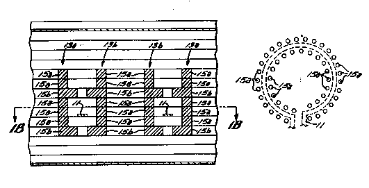
Referring now to FIGS. lA and lB, schematically
depicted therein are feLL -gn~tiC ~LLueLuLes utilized with
and distributed along the length of a ring shaped micro-
strip inAIlctAn~-e 11. Each feLL -~n~tiC structure compris-
es a pair of feIL ~n~tic via columns 13a, 13b located on
each side of the microstrip inductance 11. The via columns
13a, 13b of each f~LL~ ~n~tiC structure are generally co-
planar and extend several layers above and below the
microstrip inductance 11. As specifically shown in FIG.
lB, the feLL~ _ ic column5 13a, 13b of each ferro-
magnetic structure compri5e respective stacks of
feLL' ~netic vias that include narrow vias 15a and
inwardly extending vias 15b that are above the microstrip
inAllr~An- e 11 and inwardly extending lower wider vias below
WO 94/07349 PCI tUS93/09052
2 1L~q~6 6
-
the microstrip inductance. The narrow vias 15a can
comprise, for example, circular vias. The inwardly
extending vias 15b comprise, for example, circular vias or
line vias whose length is represented in FIG. lA and whose
width is perpendicular to the plane of the figure and can
be about equal to the diameter of narrow vias 15a.
Inwardly extending vias 15b and the intervening narrow
vias 15a of each ft:L- tic ~L-U~:LUL~ generally form
opposing C-shaped ferromagnetic ~-uuLuL~s that partially
circumscribe the microstrip inductance 11. Further narrow
fe:L., ?tiC vias 15a can extend upwardly from the inward-
ly extending vias 15b. Essentially, each f~ - tic
structure comprises a plurality of ferromagnetic vias 15
arranged to partially circumscribe the microstrip induc-
tance 11. The smaller gaps between the inwardly extending
vias 15b may be advantageous in a particular application.
While the foregoing 3-dimensional feL-. , Lic via
~LU- LUL~ has been described in the context of a ring
shaped microstrip inductance, it should be appreciated that
the f~ ic structures can be implemented with other
in~ n~ncP ,L.u- Lu~es wherein the partially circumscribing
fe~.l gnPtic via :,L-u~LuL~s are distributed along the
contour of a microstrip or stripline inductance.
The f~:L., gnPtic :~LLU~_LUL~ depicted in FIGS. lA and
lB functions to enhance in~llctAn,e and minimi7e losses due
to circulating currents induced in the ground planes. The
presence of f~rL, ?tic vias provides a preferential
media and concentration of magnetic f ield lines, which
minimizes filed line interception by the ground plane of
the unitized multilayer circuit structure and the resulting
induced currents and losses. As a result of the ferromag-
netic ~L-uuLuL~, higher inductance values are achieved,
inductor6 for a specific value can be shorter, and higher
Q is obtained.
W0 94/07349 ~! 1 2 4 1 ~ 6 PCTJVS93~09052
Referring now to FIG. 2, set forth therein is a 3-
- dimensional ferromagnetic via structure for increasing
mutual coupling between coupled lines 27, 29. The ferro-
magnetic via ~LLU~;LUL~ includes a plurality of short
feL,, gn-~1 ic via columns 23 formed in the overlap region
of coupled lines 27, 29 that are on different insulating
layers. Each of the f~LL, - -tic via columns 23 comprises
a stack of f~LL ~n"tic vias 25. The feLL~ ir.
"~L~:LU.~ allows for i ~,ved power transfer, i ~vt:d
~ ' nre transformation, as well as feedback - ~ ~ni,
~nd paths within the multilayer circuit 5tructure, in a
smaller structure.
A further application of 3-dimensional feLL, ~ ~ ic
via structures in accordance with the invention is f or EMI
isolation and shielding. Schematically depicted in FIGS.
3A and 3B is an isolation feLL Lic via structure that
includes a plurality of rows 31 of ferromagnetic via
columns 33, wherein each column comprises a stack of
f~L L, i c vias 35 . The rows 31 of f~LL ~ Lic
columns 33 essentially form a feLL. _tic isolation
region whose vertical and longitudinal extent (which is
normal to plane of FIG. 3A) will depend on the required
i601ation. The rows of fe.L~ tic via columns can be
arranged linearly with or without bends or along a contour
that is non-linear as viewed in plan view. D~r~n~inq upon
the application, the feLL, gn~tic via columns can extend
from the bottom insulating layer through the top insulating
layer, or they can be contained in certain contiguous
internal layers.
Schematically depicted in FIGS. 4A and 4B is an
isolation f~LL~ -gn~tiC via r LLu. LuLe line :,LLu~ LuLe that
inrlu~ a vertical stack 43 of line vias 45 each of which
has a length that is greater than its width . ~p~n~ i n~
upon the specific application, a plurality of vertical
stacks of line vias 45 can be used to provide isolation.
_ _ _ _ _ _ _ _ _ _ , ,, _ _, . , . , . ,, ,,,, , , , , . _ _ _
WO 94/07349 PCr/US93/090~2
-
2t a~ 8
The line vias 45 can be configured to have bends and/or
f ollow non- 1 inear contours .
FIG. 5 schematically depicts a further isolation
feLL- -gnetic via structure that includes a plurality
ft:LL- -, Lic vias 55, which can be circular vias or line
vias, for example, arranged in an interlinked grid wherein
a feL,, ~n~tic via in a given layer is partially overlap-
ping and staggered relative to any overlying or underlying
f~,,, - jl.~tiC via. For example, the grid includes verti-
cally aligned vias in f irst alternating layers and verti-
cally aligned vias in second layers, such that the vias in
the first alternating layers overlap the vias in the second
alternating layers. As shown in FIG. 5 the first or second
alternating layers can have one more group of vertically
aligned vias than the other alternating layers. The grid
can also be extended in the direction normal to the plane
of FIG. 4. l'he isolation structure of FIG. 4 essentially
forms a f~.L gn~tic isolation region whose specific
dimensions will depend on the required isolation, similarly
to the isolation f~lL~ - ic ~LLUI LUL~ of FIGS. 3A and
3B. The interlinked grid can be arranged to follow a
planar surface or a non-planar surface.
The isolation ~LUL:LULeS of FIGS. 3-5 can be used to
provide shielding on the edges of the substrate, or to
isolate circuits in one portion of the multilayer ~L,u~ Lu,e
from circuits in another portion of the multilayer struc-
ture. A f~:LLI -~ni tic ~LU- LUL~ can be arranged with bends
~ndlor curves to partially or fully enclose circuits in the
multilayer structure.
Referring now to FIG. 6, schematically depicted
therein is a f~,, gnPtic isolation structure that pro-
vides for vertical as well as lateral isolation. A row of
f~ tic via columns 63 is located between correspond-
ing terminal edges of first and second planar f~:LL , etic
layers 67, 69, wherein such row includes a plurality of via
WO 94/07349 2 1 ~ 4 1 ~ 6 PC~/US93/09052
columns arranged similarly to one of the via column rows in
~ the structure of FIG. 3B. The ferromagnetic layers 67, 69
are formed by screen printing a compatible ferrite ink on
the associated insulating layers . DPpPn~l i n~ upon the
application, the isolation :~LU~ LULe between the first and
second planar feL, -~nPtic layer5 can extend along further
c.,~.~7~ ~lin~ edges of the planar layers as reguired. The
isolation structure between the f irst and second planar
fe~ -tic layers can also comprise multiple rows of
feLL -gnPtic via columns as described above relative to
FIGS. 3A and 3B, or an interlinked fCLL~ r via grid
as described above relative to FIG. 4, As a further
alternative, a fcL~, -gnPtic line via wall structure as
described above relative to FIG. 5 could also be utilized
with the first and second planar fe~L~ ~ tic layers.
P~eferring now to FIG. 7, schematically depicted
therein is a fc~LL~ gnPt ic via band that encircles a
conductive trace 71 for ~h~n~in~ line i ~ . q'he
feLL~ gn~tic via band comprises a plurality of interlinked
feLr, , -tir vias 75a, 75b, 75c of different lateral
dimensions arranged so that a continuous band of ferromag-
netic material fully encircles the conductive trace. For
in.iL.as~d current handling, parallel conductor traces can
be utilized with common f el L ~ , tic bands or separate
fcl~ ic bands. The vias 75a, 75b, 75c can comprise
circular vias of different .1; ~Prs or a combination of
line vias for the vias 75a, 75b of greater lateral dimen-
sion, and circular vias for the vias 75c of lesser lateral
dimension, as depicted in FIG. 7B. In the configuration
that includes line vias and circular vias, the widths of
the line vias can be about the same as the diameter of the
circular vias, for example.
FIGS. 8A and 8B schematically depict a further embodi-
ment of a f~L~ 7netic band that in~ PC vias of
different lateral dimensions, wherein top and bottom vias
. . _ . _ . _ . . _ _ . . _ _ _ _ _ _ _ _ _ _ _ _ _
WO 94/07349 PCI /US93/090~2
.
~12
81a have greater lateral dimensions than vias 81b arranged
in respective columns at the lateral ends of the top and
bottom vias 81a. As particularly depicted in FIG. 8B, the
vias 81b can comprise circular vias, and the top and bottom
vias 81a can comprise line via5 whose widths are about the
same as the diameter of thQ interposed circular vias.
It should be appreciated that one or more of the
f~rL ~n,-tic bands could be used on a particular line,
d~p~n~ing upon the application and its requirements,
current, frequency, material properties, and so forth.
Particular applications include high frequency noise
filtering, harmonic control, radiation ~ul~L~ssion, and
wave shaping.
Fe.r, -~n~tic via structures in accordance with the
invention are made, for example, pursuant to low tempera-
ture co-fired proC~scin~ such as ~ secl in "Development
of a Low T~ a LUL ~ Co-f ired Multilayer Ceramic Technolo-
gy," by William A. Vitriol et al., 1983 ISHM Procee~3in~
pages 593-598; "Processing and ~ hil ity of Resistors
InouL~uLated Within Low T- ~LuLe Co-flred Ceramic
5Lr uuLuL~, " by Ramona G. Pond et al., 1986 ISHM Proceed-
ings, pages 461-472; and "Low Temperature Co-Fireable
Ceramics with Co-Fired Resistors," by H. T. Sawhill et al.,
1986 ISHN Proc~e~lin~, pages 268-271.
2 5 In accordance with low t~.. "e~ ~ Lu. ~ co-f ired process-
ing, vias are formed in a plurality of green thick film
tape layers at locations defined by the desired via config-
urations of the desired multilayer circuit. The vias are
coated or f illed with the appropriate f ill material, f or
example, by screen printing. Conductor metallization for
conductive traces including the stripline conductors and
the ~ he~lA~ ground planes are then deposited on the indi-
vidual tape layers by screen printing, for example, and
materials for forming passive --ts are deposited on
the tape layers. The tape layers are laminated and fired
_ _ _ _ _ _ .
wOs4/07349 ~ ~4 1 ~6 Pcr/uSs3/osoS2
.
11
at a temperature below 1200 degrees Celsius (typically 8s0
degrees Celsius) for a predetermined length of time which
drives of f organic materials contained in the green ceramic
tape and forms a solid ceramic 5ubstrate. External metal-
lization including the lower ground plane r ~ ~ l i 7Ption and
any side wall metallization can then be applied by known
techniques .
FeL~I ~, ic via ~L.u-,~uLes in accordance with the
invention can also be implemented with other technologies
for forming unitized multilayer circuit ::~LLuuLuLes~ includ-
ing for example high temperature co-fired ceramics, hard
ceramic multilayer single firing tP~hn~logy, and a laminat-
ed soft substrate approach.
The foregoing has been a disclosure of ft:LL~ , -llc
~LLU~.:LUL~S that are advantageously il.c~ L~lted in unitized
multilayer circuit ~LLU~;LULèS and are fabricated util17ing
processes for forming unitized multilayer circuit struc-
tures .
Although the foregoing has been a description and
illustration of specific Pmhorli- LS of the invention,
various modif ications and changes thereto can be made by
persons skilled in the art without departing from the scope
and spirit of the invention a5 defined by the following
claims .