Note: Descriptions are shown in the official language in which they were submitted.
21~4~~%
1
IMPROVEMENTS TO DEVICES FOR MANUFACTURYNG ELECTRETS, AND
ELECTRETS OBTAINED THEREBY
The invention relates to electrets, i.e. to
dielectrics that are permanently electrically polarized
because they carry permanent electrical charge.
More particularly, it relates to those electrets
that are in the form of sheets or thin layers and usable,
in particular, for building electromechanical transducers
(microphones, accelerometers, pressure sensors, etc.) or
electrostatic relays.
The invention relates in particular to devices for
manufacturing electrets of the kind in question.
With known methods of manufacturing such electrets,
it is very difficult to obtain uniform distribution of
the electric charge carried: charge density is much lower
in the vicinity of the edges of the electret than in the
center, and may even be zero.
Such lack of uniformity gives rise to various
drawbacks, in particular with respect to the sensitivity
and/or the stability of transducers or relays built on
the basis of the corresponding electrets.
To remedy that drawback, i.e. to obtain uniform
distribution of electric charge over the entire charged
face of the electret, including right up to its edges,
proposals have already been made to place a diaphragm a
short distance from said face while it is being charged,
the diaphragm carrying electric charge of the same sign
as the charge being implanted, and the opening in the
diaphragm corresponding to the area to be charged.
That method requires relatively exact positioning in
all directions between the diaphragm and the face to be
charged, and in the implementation of said method as
described in an article by Heinz Von Seggern, published
on pages 1623 to 1626 of IEEE Transactions on Industry
Applications, Vol. lA - 20,November 1984, New York, the
area to be charged was single and separated from the
2
diaphragm by a distance of about 1 millimeter and had a
surface area of much more than 10 cmz.
A particular aim of the invention is to improve the
charging methods and devices in question, in particular
by making them easily applicable to manufacturing thin
sheet electrets of relatively small dimensions, the
greatest of said dimensions being less than 1 cm and
preferably less than 6 mm: this applies to numerous Si02
electrets which are often in the form of small
rectangular plates having dimensions of about 2 mm to
3 mm.
To this end, devices for manufacturing electrets of
the kind in question still comprise an electrode for
supporting the dielectric that is to be charged in order
to become an electret, means for generating electric
charge and for entraining it towards the dielectric, and
a frame disposed close to the periphery of the
dielectric, which frame is constituted and installed in
such a manner as to carry electric charge of the same
sign as the charge being implanted in the dielectric, at
least while the dielectric is being charged, and they are
characterized in that the said frame forms a single block
with the electrode.
Thus, there is no longer any risk of the frame being
wrongly positioned relative to the electrode while ~ths
dielectric is being charged, the resulting assembly is
robust overall and it lends itself easily to simultaneous
manufacture of a plurality of small-sized electrets
having remarkable uniformity in distribution of the
implanted electric charge, right up to the margins of the
charged faces.
rn preferred embodiments, use is also made of one or
more of the following dispositions:
the frame is electrically conductive and is
insulated from the electrode by a solid electrically-
insulating layer;
L
3
in a device according to the preceding paragraph,
the frame forms an integral portion o~ a conductive plate
itself supporting tha electrode with an insulating layer
being interposed therebetween;
in a device according to the paragraph before the
preceding paragraph, the frame is pierced by an opening
in which it receives the electret and is placed on the
electrode with an interposed insulating layer;
the frame is constituted by a dielectric suitable
for receiving permanent electric charge, as is the
dielectric surrounded by said frame; and
the frame itself forms a portion of a grid or
perforated layer or sheet designed for simultaneous
manufacture of a plurality of electrets, and defines one
of the meshes thereof.
The invention also provides electrets obtained by
means of the above devices, which electrets have highly
uniform surface charge, even at their margins, said
electrets advantageously implementing at least one of the
following characteristics:
each of the two long dimensions of the charged thin
layer or sheet is shorter than 6 mm; and
the charged thin layer or sheet is made of SiOZ.
In addition to the above dispositions, the invention
comprises certain other dispositions which are preferably
used simultaneously therewith and which are described in
greater detail below.
Three embodiments of the invention are described by
way of non-limiting illustration, and with reference to
the accompanying drawing.
The three figures in the drawing are respective
diagrams of three devices used for charging electrets and
each of them is implemented in accordance with the
present invention.
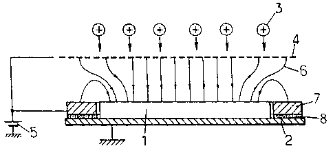
In each of-these devices, there can be seen a
dielectric 1 to be charged which is present in the form
of a thin layer or sheet, advantageously made of Si02,
and an electrode plate 2 that is grounded and against
which the dielectric is placed, which plate may be made
of silicon.
Ions 3 to be implanted in the dielectric 1 may be
created in the environment of said dielectric in any
appropriate way, e.g. by means of an electron gun, or by
means of a driving electric field.
In each of the embodiments described below, the ions
3 are created by the corona effect, and the ions 3 are
accelerated towards the dielectric through a grid 4 which
is raised by means of a voltage source 5 to a potential
that is close to the surface potential which it is
desired to obtain for the electret. The electric field
lines followed by the ions 3 are referenced 6.
In the first embodiment shown diagrammatically in
Figure 1, there can also be seen a conductive frame 7
placed on the electrode 2 with an interposed insulating
layer 8 around the dielectric 1 and almost in contact
therewith.
The frame 7 is electrically connected to the grid 4
so as to be raised to the same potential as the grid.
The presence of the frame 7 raised to the indicated
potential all around the edges of the dielectric 1
' prevents any deflection or leakage of ions 3 towards the
overhanging periphery of the el2ctrode 2.
on the contrary, the frame ~ plays the same role as
the grid 4 with respect to driving ions 3 towards the
dielectric 1.
In the end, the distribution of permanent electric
charge implanted in the Final electret is uniform over
the entire charged area of said electret, including at
its margins.
The frame 7 may be fixed permanently to the
electrode 2, with electrical connection between the frame
and the electrode being established after the electret
has been charged.
CA 02124294 2001-04-18
If, as assumed above, the electret 1 is made of
SiO~, and the substrate electrode 1 is made of silicon,
then the frame 7 may be constituted by the frame that is
commonly used for ensuring final adhesion between said
5 substrate 1 and another sheet or plate of silicon (not
shown) covering the entire assembly and appropriately
micromachined, said frame 7 then advantageously being
made of gold or of a gold alloy.
In a variant, provision may be made for the frame 7
to be placed on the electrode 1 in temporary manner only
so that it is removable after charging.
In the embodiment described above, the final value
U1 obtained for the surface potential of the electret is,
in theory, equal to the potential to which the grid 4 was
raised during charging.
In practice, this final value may be slightly
greater than the potential of the grid since accelerated
ions may have sufficient kinetic energy to go through the
grid even when the electric field that exists between the
grid and the surface of the electret has become zero, so
that they continue to be deposited on the electret even
after equal potentials have been established.
Under such circumstances, while charging is taking
place, it is appropriate to raise the frame 7 to a final
value of potential UZ that is slightly greater than U1.
By way of example, if the electrode 1 is put to a
potential Uo of zero volts, then the tensions U1 and U~
may be made respectively equal to 200 volts and
220 volts.
In the second embodiment shown diagrammatically in
Figure 2, the dimensions of the electrode 2 on which the
dielectric to be charged is placed are identical to the
dimensions of the dielectric, and the assembly is itself
deposited on a conductive substrate 9 with an intervening
insulating layer 10.
CA 02124294 2001-04-18
6
The substrate 9 is raised to the potential U1 as
defined above, and it is dimensioned so as to project
outwards all round the assembly of dielectric 1 and electrode 2.
In this case, it is the edges of the substrate that
play the role of the above-described frame 7: these edges
are not accurately disposed "around" the dielectric 1,
i.e. on the same level as the dielectric, but the
correcting electrical role that they play relative to
peripheral ions 3, i.e. urging them towards the dielectric
1, is entirely analogous to the above.
Here again, means may advantageously be provided as
represented by dashed lines 11 for the purpose of
electrically connecting the substrate 9 to the electrode
2 after the electret 1 has been charged.
In the third embodiment shown diagrammatically in
Figure 3, the frame referenced 12 is made of a dielectric
material identical or analogous to that constituting the
dielectric 1, i.e. capable like that dielectric of
trapping electrical charge sprayed onto its surface.
Everything then takes place as though the frame 12
itself constitutes the periphery of a larger dielectric
with charging taking place conventionally.
The main difference between the two processes lies
in the fact that in the present case, said "periphery" of
the enlarged dielectric which ends up less charged than the
remainder of said dielectric, i.e. the remainder
constituting the central portion of the enlarged dielectric
and designed to become the final electret, can be
separated from said remainder at the end of charging
since it is constituted by the frame 12 itself which is
independent of the electret being formed 1.
In this case, as in the cases of Figures 1 and 2, it
can be observed that during charging of the dielectric 1
the frame 12 carries a certain amount of electric charge
having the same sign as the charge to be implanted in the
dielectric, which charge in the frame is suitable for
electrically opposing "leakage" towards the electrode 2
7
of the charge that is to be implanted in the periphery of
the dielectric.
It may also be observed that the presence of the
frames 12 itself distances the electrode 2 from the edges
of the dielectric 1, thereby correspondingly reducing the
above-mentioned tendency to leakage.
Dispositions are advantageously taken to enable the
frame 12 to be effectively separated after the electret
has been charged, it being possible to interpose an anti-
adhesive layer (not shown) between said frame and the
electrode 2.
The thickness of the frame 7 or 12 may be equal to
the thickness of the electret 1. Alternatively it may be
less than or greater than the thickness of the electret
1.
The width of the gap between the electret 1 and the
frame 7 or 12 surrounding the electret may be zero; it
may be non-zero, in which case it is preferably less than
the distance between the grid 4 and the facing face of
the electret 1.
As a result, and regardless of the particular
embodiment used, methods and devices are finally obtained
for charging electrets that enable remarkably uniform
distribution of the implanted electric charge to be
obtained for the electrets in a manner that is very
simple, said uniformity extending sight up to the edges
of the electrets, thereby achieving excellent qualities
of sensitivity and/or stability, and this applies even if
the electrets are small in size, having a maximum
dimension of less than 6 mm.
Naturally, and as can already be seen from the
above, the invention is not limited in any way to those
applications and embodiments that have been described
more particularly; on the contrary, it extends to any
variants, and in particular:
21~~~2~~
8
those in which the electrode that carries the
dielectric to be charged is raised to a fixed potential
Uo other than the zero potential of grounds and
those in which the frame itself forms a portion of a
grid or of a perforated layer or sheet designed for
manufacturing a plurality of electrets simultaneously,
the frame outlining one of the meshes therein.