Note: Descriptions are shown in the official language in which they were submitted.
.\
~~~4880
The present invention relates in general to power
control apparatuses and, in particular, to a power
control system for measuring the current drawn by a
power amplifier which is indicative of its power
output and altering the input to the power amplifier
so as to alter its power output.
Power amplifiers are used in radio transmitters
to produce a signal with sufficient power for trans-
mitting over a distance. Most, if not all, radio
transmitters measure the power output of this ampli-
fier, toward being able to adjust the output of this
amplifier to match a desired value. The most widely
used approach to accomplish this measurement uti-
lizes a directional coupler on the post power ampli-
fier transmission line which is connected to a diode
detector. Overall, this approach is expensive to
implement, both financially and in terms of space
requirements. This is particularly true in high
frequency radio applications where Schottky diodes
-- which are rather expensive -- would be necessary
to provide an accurate measurement of minor varia-
tions in power amplifier output.
Current mirrors have long been utilized in elec-
trical circuits as a current source device. Partic-
ularly in integrated circuits, multiple current
mirrors are used to '°steer" an externally generated
current in various multiples of the known generated
current to various portions of the circuit. These
uses of the current mirror all require a constant
current source to supply the mirror with a known
programming current, which, in turn, sets the var-
ious currents.
Another approach to power output measurement
measures the operating current drawn by the power
amplifier. The operating current drawn by the power
2
,.
.>.. . . ' . ;.::: '"~ ' .': . .' %, '' r: , . . ;'~. . .... ... . - '
. .. . ;., , .I .'. ,. .. .. :. " ;r , ;: . ~;:". .. ;:, . v. ~; :.
.,. . :::.. ,. :::, , ; ". .'. , .. .,.: .: .
, , , ~, ... '
. .,. , '
~'
,. ;:. , .
. :::;,.. .., ; ~'.. ~~:~ }. -.::: ... .. .
. ...:--. . ." :: :
. ..:: ..: .:. ;.., ; ,:. ... -.. : :.: :'
;:..: ::.:; ~;.: "."
' ,;. .,
~ (
.
.
.
~
.,.: . , .::. : ,.., . . ,:.: ,
;;.,;; . ;,:. ; .;-: :: ,; "
"": .., . ,:: " ,:. ;i :...
. . ~ :. ,:. . :
;, .: ,
v:
. ;; I s :. ,v: ..
,
i,;::
,~~
. . , .. ,,
t, f f ",I
'
~:.
.:
; (:~. ,.
, ~. t ,I .
(
a r: : :,,. .
.:i :
: n ,.
I
~ , r: l :.': !'
v . r ':fu r
. 1,., r : ' :' CI
: '
f ~ '
' '.
'
.
r
r
~
. , .
. I;
:i. i. , . ;,
r tu. . . , .
:;At.: . .~ r . .;~>' ~ ." l r .
...', ':' ~r' 1 . . ,.,
, i a-,,~,In..... ..
, .. .:. ..:
,- '' r .;~. ,
,~r W :"-
:,'~.:: I
'':!' (
~
~
" , ..r ,
.: .: , ..
. : ;'. I ~ .. I '
~ !.; . . .
.
.
:
~. (
;.
..
'. , . . ;:' :.; '
,., ,
amplifier is related to the amplifier output power,
or gain, such that measuring the current drawn by
the power amplifier may be used to determine its
output power. This approach is valid for class B, C
or BC power amplifiers. These power amplifier class-
es draw an operating current proportional to their
power output. The measurement of this current can
be accomplished in various conventional ways, such
as inserting a resistor in the source line and
measuring the voltage drop across the resistor using
an operational amplifier; an expensive approach.
The introduction of a resistor into this line dimin-
fishes the power received by the power amplifier. Of
course, the value of the resistor can be minimized
to minimize power dissipation, however, this would w
be at the expense of requiring a more sensitive
operational amplifier, which is increasingly expen-
sive given increased sensitivity.
It is thus an object of the present invention to
provide a low-cost approach to measuring the power
output of a power amplifier.
It is a further object to provide a measuring
approach which introduces a minimal voltage drop
into the connection between the power source and the
amplifier.
These and other objects will become apparent in
light of the attached specification and drawings.
A preferred embodiment of the invention comprises
a power control system for controlling the power
output of a power amplifier. The power control
system draws power from a variable voltage supply,
such as a battery, and receives a signal input which
indicates the desired output of the power amplifier.
The power control system includes power amplifier
~1~4~~0
means for amplifying an electrical signal wherein the
power amplifier means draws an operating current
From the variable voltage supply. The power ampli-
fier means is of the type wherein this drawn current
is indicative of the power output of the power
amplifier means.
The power control system also includes current w
sense means operably connected between the variable
voltage supply and power amplifier means for sensing
the current drawn by the power amplifier means and
simultaneously producing an output signal, which is
directly correlated to the sensed drawn current.
The power control system further includes control
means which operably accepts the output signal from
the current sense means and a signal input toward
comparing the two signals so as to produce a control
signal for controlling the power output of the power
amplifier means.
In a preferred embodiment, the current sense means
is configured so as to minimize the voltage drop
between the power amplifier means and the variable
source voltage to, in turn, minimize the draw on the
variable voltage supply. This preferred embodiment
includes two matched transistors; a first transistor
with its emitter connected to the variable voltage
supply and collector connected to the power amplifi-
er, and a second transistor operably connected by
its emitter to the variable voltage supply and by
its base to the base of the first transistor. The
bases of the first and second transistors are fur-
ther coupled to the collector of the first transis-
tor. Thus, in this embodiment, the sensed current
travels through the-first transistor and the output
signal is outputted from the collector of the second
transistor.
4
~124~80
In this embodiment, the current sense means may
further inrrlude ratio means electrically connected
to the second emitter fox setting a ratio between
the current drawn by the power amplifier means and
the current output by the second transistor which
may comprise a resistor or may involve adjusting the '
relative sizes of the emitter junctions of the first
and second transistors. In a preferred embodiment,
the ratio is chosen to minimize the draw on the
variable voltage source and further to minimize
temperature concerns.
In this preferred embodiment, the apparatus fur-
ther includes a current-to-voltage converter means,
which may comprise a resistor, for converting the
sensed current into a sensed voltage. This resistor
may be chosen so as to offset any temperature ef-
fects in the operation of the first and second
transistors.
In a preferred embodiment, the current sense means
outputs a voltage to the control means. In this
embodiment, the control means includes a comparitor
transistor, its base connected to the signal input,
which is a voltage set point, and its emitter con-
nected to the sensed voltage from the current sense
means. The collector of the comparitor transistor
is operably connected to an exciter through a pro-
tection resistor which protects the bias control
transistor of the exciter. The control means fur-
ther includes a charge-up resistor operably connect-
ed between a supply voltage and the protection
resistor. The control means additionally includes a
capacitor operably connected between the protection
resistor and ground, so as to prevent oscillation of
the apparatus by providing a delay in combination
with the charge-up resistor and the protection
~~~~~~o
resistor.
In a preferred embodiment, the control means
further itlcludes a switching transistor operably
connected between the comparitor transistor and the
protection resistor. The base of the switching
transistor is tied to an activation signal, which
indicates whether the power amplifier should be
enabled.
In operation, when the power amplifier means draws
a first current from the variable voltage supply,
the current sense means draws a second current from
the variable power source wherein the first current
is a multiple of the second current, based upon the
value of the ratio means. The second current is
converted into a first voltage by a resistor whose
value has been chosen to compensate for any tempera-
ture variance in the current sense means. This
first voltage is then compared with the predeter-
mined power setting -- represented by the signal
input applied to the comparitor transistor -- re-
sulting in a second voltage which is applied to bias
the power amplifier means toward altering the power ~-...
output of the power amplifier means.
Fig. 1 of the drawings is a block schematic dia-
gram of a prior art current mirror showing, in
particular, a constant current source programming
the current provided to a load;
Fig. 2 of the drawings is a schematic block dia-
gram of the present power control system;
Fig. 3 of the drawings is a schematic diagram of a
preferred embodiment of the control means;
Fig. 3A of the drawings is a schematic diagram of
a second embodiment of the control means; and
Fig. 4 of the drawings is a schematic diagram of
6
the exciter showing, in particular, the interconnec-
tion of then control means and the exciter.
While this invention is susceptible of embodiment
in many different forms and in many different sys-
tems, there is shown in the drawings and will herein
be described in detail, one specific embodiment in
one representative system with the understanding
that the present disclosure is to be considered as
an exemplification of the principles of the inven-
tion and is not intended to limit the invention to
the embodiment or the system illustrated.
Fig. 1 of the drawings is a schematic diagram of a
prior art current mirror. The mirror shown in Fig.
1 is programmed by constant current source 10 by it
sinking a known current, Icon, from the collector of
transistor 11 resulting in a current in transistor
12, being used to source load 13. The value of the
current source by transistor 12 is a function of the
value of resistor 14.
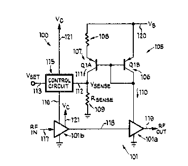
Fig. 2 of the drawings is a schematic block dia-
gram of power control system 100 of the present
invention. Power control system 100 controls the
power output of power amplifier means 101. In a
preferred embodiment, power amplifier means 101 is
comprised of power amplifier 101a and exciter lOlb.
Power amplifier lOla may be a class B, C or BC type
amplifier wherein the current drawn by power ampli-
fier 10~1a from variable voltage supply 120 is indic-
ative of its power output. In a preferred emboli-
ment, power amplifier 101a is a class BC amplifier
which draws no current whatsoever unless it is
driven by exciter lOlb.
Exciter lOlb is a class A amplifier forced to run
in compression, i.e. non-linear mode, by providing
2124:880
RFin 117 to have such power that the power of exciter
output 1181 is compressed. The output of exciter
101b is operably connected to and drives power
amplifier 101a which draws a current from variable
voltage supply 120.
Variable voltage supply 120, which may comprise a
battery (not shown), may be used to power control
system 100, as well as any electrical circuitry in a y
product utilizing apparatus 100. Tt is possible,
though, for control means 115 and exciter 101b to be
powered by separate supply voltage 121, which must
only be greater than Vsense 112, so that control
means 115 and exciter 101b can operate properly.
Power control apparatus 100 further includes
current sense means 105 for sensing sensed current
110 drawn by power amplifier means 101 and simulta-
neously producing output current 111. Output cur-
rent 111 which is also drawn from variable voltage
supply 120 is directly correlated to sensed current
110. Current sense means 105 is operably connected
between variable voltage supply 120 and power ampli-
fier means 101 and is configured to minimize the
voltage drop between variable voltage supply 120 and
power amplifier 101a of power amplifier means 101.
In a preferred embodiment, current sense means 105
includes first transistor 106 and second transistor
107, which are matched -- and preferably reside on
the same IC chip so as to minimize temperature
variatilons. The emitter of first transistor 106 is
operably connected to variable voltage supply 120
and the collector is operably connected to power
amplifier 101a. The base of first transistor 106
and base of second transistor 107 are also operably
connected together and also to the collector of "
first transistor 106. In this embodiment, the
8
?~.24~~0
emitter of second transistor 107 is operably connect-
ed to variable voltage supply 120 through ratio
means 108,. which may be a resistor, but may instead
involve varying the relative emitter junction sizes
of first transistor 106 and second transistor 107.
In operation, second transistor 107 is programmed
by sensed current 110 which is drawn by power ampli- -
fier lOla through first transistor 106. Because
power amplifier lOla is of the type in which the
drawn current is indicative of its output power,
sensed current 110 indicates the power output of
power amplifier means 101. Output current 111 is a
multiple of sensed current 110 dependent upon the
value of ratio means 108. In a preferred embodi-
ment, ratio means 108 is set such that output cur-
rent 111 is approximately one-tenth sensed current
110 to further minimize the draw of variable voltage
supply 120 and minimize temperature concerns.
In a preferred embodiment, output current 111 is
converted to Vsense 112 by current-to-voltage con-
verter means 109, which may comprise a resistor
electrically connected to ground. Resistor 108 may
additionally be chosen so as to offset any tempera-
ture effects in the operation of first transistor
106 and second transistor 107. In a preferred
embodiment, Rsense 109 is one hundred and twenty '
ohms.
Power control apparatus 100 finally includes
control means 115 fox comparing Vsense 112 to Vset
113, so as to produce bias control signal 116 for
controlling the power output by power amplifier
means.101. In a preferred embodiment shown in fig.
3, control means 115 includes comparitor transistor
130, which compares Vsense 112 to Vset 113. The
base of comparitor transistor 130 is operably con-
9
,.
':,' : .: . ': . ,
. , . ;. .
r .: : ,, ..,~, , :~ , ; . J , .
.; ° . .
. ;; .. . , . -, . ; " , ,, . ~ . ., ..,
.~, J , .f':: 'r~Vi:.: ~i::;l;. au, ..
e.? 1. ..~u 1...
.J''.. , ,~t
"',lt t 9~" :,lJl v r~' i;~u
rs#S. . ~~:'~ . . .,....,,~., . , ,,,y ~,!dw,, i,., ~r' ",. "%, .~,.. s i ,
,~,.,~;;. , dl,S ;' . . r><r ,. ., rr Sw. ~ .. ,4~I ~rr, 6lrM'9.%. ~,~?~~~;,:,
9 ,. s ~ ?~ ~ ,..~r. , ,.'-~f~'~' . e,r:, , ~.i;~r
~~24~~0
nected to Vset 113 through a base protection resis-
tor. Vset 113 may be produced by any number of
sources, such as a microprocessor having a digital-
to-analog converter output. The emitter of compari-
for transistor 130 is operably connected to Vsense
112 such that the collector of comparitor transistor
130 sources an output indicative of the required
power change. The collector of comparitor transis-
for 130 is operably connected to protection resistor
132 which protects bias control transistor 140 of
exciter 101b (shown in Fig. 4). Bias control signal
116 is fed directly into power amplifier lOla. In
another embodiment, bias control signal 116 can be
fed into a stage prior to power amplifier means 101,
wherein it can affect the power of RF in 117. In
this alternative embodiment, protection resistor 132
would still be included for its use as a time con-
stant.
Control means 115 further includes charge-up
resistor 133, which is operably connected between
supply voltage 121 and protection resistor 132.
Supply voltage 121 can be any value greater than
Usense 112, including the same value as variable
voltage supply 120. Supply voltage 121 must also be
supplied to exciter 101b for the circuit to operate
correctly. Charge-up resistor 133 and protection
resistor 132 individually, in combination with
capacitor 134, prevents oscillation of control means
115, and in turn apparatus 100, by providing a
delay, such that transient power changes -- includ-
ing current charges caused by control means 115 --
are ignored unless maintained.
In a preferred embodiment, control means 115
further comprises switching transistor 131 operably
connected between comparitor transistor 130 and
w..
,rv..~Y. ~..::: , <.,f :r:.
, .y.
Y "%
,.P ., s..4....
,~ . P. .
r. .... . .. ..
. T~F~;. ,~:H~F' '..;,a ..:. r .~S . .
?. ",.;
, ~.~(' . % , .,. .. :;
i . .. L..~Si ..
'~ ,.:,;! .:.x
, Y ,
,:. .
~
~
.
r .
. ,
. ..,, . ",.,., , .
. ';
! , o..:
f Jr
f
,,..:.;, ., :~. ,:..,., . ~.;'~.- '.:"~:.
. ,.
~
::. . ,::: ; .:~...,:: .;!,.. :: ..r~:. , :..,, :. .. . ;,.:: . . .:;.,
. .. . ; ~ :.:::., ~.:
,::,: : . ' .:';
..J : :
.
'
,.._.:. ~":,. .... -;~:~., .: :...:'.: ;..:,;
' . ' . :.: .. , ..,.:
,.,...: .: r ' ,
, ,';',. ' .; ~..-
,. .','..;. .. ; : ~' ..
.,. . ~ .~ ':.::. . ..::~. .
i:, : ,,"' ...::':;: y.::,, . ..,.,
~ :
~~ fir..:
' ..
;
.,
'~: ,~ ~: -: ,
w..
~
.:~
.
;
~
~
:
;'
~ ~:
'
. . , ,
, . ., :
. .... . .
..,:.,. ,.:: i. . ~.~.: .: v.
. , W :.. ..
.. , J :. .
:.::. , J. .: , ,. ;: .
':.. . . .....;~:. .
., , .
t / J :
, .
. .;. .
..,
.:. ,
:
.,:~:' ...: n.~,. '.:,~', :::: ::~ ~ ~..
w;
.,.,
! 7. .,
'
.. . , .: , .,;, ,., . . .
t;. . . , ,
.. JJ , 7 . r.. ',:.. ::.; , .;~ .. , ,::',', ; '.
a ; . r ,~ '. ..:. .'.:.. ,
:. ~ : ,J...., . j..:.
''.., .:.
.~~:~.
.
'
:i;
;
:~;
s'::
.
. ; ...
, 1 .
Jh ' . .
.
, .
'
.., :.
.
J f. ..: . , ..
,'-!;., :.': ,. .~:' ...: ~:.. :;.. :'.' .i.'~ n ~....' ~~. :, :...,~:.
..': .. . , , .. :' ,. .... .
.::~ W
'
,' 1 ' . .
~ ,
J ','. .
: ,j , .
... ~j .~ .j, J:."~
J .~,i 1 y: . ,
~~.2~8~0
protection resistor 132. The base of switching
transistor 131 is connected to Von 135, which indi-
cates whether power amplifier means 101 should be
enabled. For instance, in a radio system which
partially powers down while idle, Von 135 is used to
turn the transmitter off so it does not needlessly
drain power. In a second embodiment, shown in Fig.
3A, competitor transistor 130 and switching transis-
for 131 are combined into one transistor by utili2--
ing a summer circuit consisting of Vset 113 divided
into three components each of which are fed through
weighted resistors R1, R2 and R3 and Von 135 which
is fed through resistor Ron.
Fig. 4 is a schematic diagram of exciter 101b
showing, in particular, the interconnection of
exciter 101b and control means 115. As is shown,
bias control signal 116 from control means 115 is
fed into the base of bias control transistor 140.
This serves to alter the power output of exciter
lOlb, which in turn alters the power output by power
amplifier 101a. It is possible, of course, to
maintain a constant bias voltage on bias control
transistor 140 and feed bias control signal 116,
which is a bias voltage, directly into the RF signal
either before it enters exciter 101b or before it
enters power amplifier lOlb. This is particularly
true because of the flexibility of Vset 113 and
Vsense112~ In a preferred embodiment, Rsense 109
has been chosen to compensate for temperature varia-
tions. Thus, at the expense of losing temperature
compensation, Rsense 109 can take almost any valve
and, in turn, allow Vsense 112 take any value which
when compared to Vset 113 can provide any desired
bias control signal 116.
The foregoing description and drawings merely
11
~~~~~~o
explain and illustrate the invention and the inven-
tion is not limited thereto, except insofar as the
appended t;laims are so limited and as those skilled
in the art who have the disclosure before them will
be able to make modifications and variations therein
without departing from the scope of the invention.
12
N,