Note: Descriptions are shown in the official language in which they were submitted.
2125040
A PROCESS AND AN APPARATUS FOR WAVE SOLDERING
The present invention relates to wave soldering of
elements such as printed wiring boards and more
specifically to solder coating of wettable metallic
surfaces or joining at least two wettable metallic
surfaces on wiring boards in a solder wave wherein the
wave is blanketed with a reduced oxygen gas atmosphere.
Printed wiring boards, circuit boards and other
elements now have smaller wettable surfaces to be solder
coated and joined. Whereas in the past flux was used to
remove oxides from these surfaces, it has now been found
that if soldering occurs within an inert gas or a shield
gas atmosphere which excludes oxygen, then flux may not
be necessary. In the present application, the term
"inert" as applied to gas includes nitrogen. Furthermore
dross and other oxides do not form on the surface of
solder in an inert atmosphere. In the past dross and
oxide particles have caused skips, bridges, or other
defects to occur in soldered joints.
In U.S. Patent 5, 048,746 is disclosed a tunnel for
fluxless soldering. In U.S. Patent 5,044,542 iS shown
shield gas wave soldering. In both cases solder is
applied to an element in a shield gas environment. The
shield gas may be inert gas or a reducing gas which
excludes oxygen. The benefits of soldering in an
atmosphere which excludes oxygen are known.
Tardoskegyi in U.S. patent 3,705,457 and Elliott
et al in Canadian patent application 2,155,351 both
disclose the use of a gas knife jet. U.S. patents
4,402,448, 4,679,720 and 4,995,411 all assigned to Hollis
Automation Inc. disclose the uses of gas or air knife
, ~ ..~ .
.. f -!J
_~093/1l6~ 212 ~ PCT/CA92/00~'~
-- 2 --
jets for cleaning surface mounted conductor elements
carried by printed circuit boards.
One of the problems with flux in the past is that
the flux itself caused a deposit or residue on the solder
coated surfaces after solder coating and this residue
generally had to be removed by cleaning after soldering.
However, flux technology has improved and it is now
possible to use what is sometimes referred to as a "no-
clean" flux which does not leave a residue and does not
require solder coated surfaces to be cleaned after solder
coating. The term "no-clean" flux is applied to a flux
which leaves a low level of residue on solder, the
residue generally being non-corrosive and non-conductive.
One example of a no-clean flux contains little or no
halide, another example is a non-corrosive and non-
conductive organic acid dissolved in an ethanol or
isopropanol solvent. A further example is common RMA
flux which is a mixture of a rosin, such as abietic acid,
an activator, such as divethylamine hydrochloride and
solvent such as alcohol.
The addition of a small quantity of adipic acid with
a solvent such as ethyl or isopropyl alcohol results in a
no-clean flux. Furthermore, it is known that low dross
solder, which contains from about 10 to 1000 ppm
phosphorous, reduces dross formation in a solder pot
exposed to air. By utilizing a low dross solder it has
been found that the shield gas used to blanket a solder
wave during solder coating does not require all oxygen to
be removed from the atmosphere. A satisfactory solder
coating can be obtained with low dross solder when an
oxygen content of about 5% is included in the shield gas.
In some situations oxygen contents greater than 5~ are
satisfactory. Thus the cost of a shield gas is greatly
reduced, and this results in savings in the soldering
process.
21250~
_~093/116~3 - PCT/CA92/00~23
-- 3 --
In the present invention, it has been discovered
that utilizing a cover, shroud or the like at least
partially covering a solder reservoir and blanketing with
a shield gas from within, one is able to reduce air to
almost negligible amounts from the solder wave and around
an element such as a wiring board and the like. Thus,
wettable surfaces to be solder coated, such as circuit
tracks, pads and metallized holes in boards with pins
therein are kept substantially free of air. Furthermore
the solder surface under the cover, and the solder wave
surface are kept free of air avoiding dross forming on
the solder wave and in many cases avoiding the necessity
of having to use flux in the solder coating step.
It is an aim of the present invention to provide a
cover or shroud to at least partially cover a solder
reservoir and blanket the solder wave and solder within
the reservoir with a shield gas. At least one, and
preferably two or more solder nozzles are used with each
solder wave having its own independent wave height
control and shield gas flow control. Several narrow
solder waves are easier to blanket with shield gas rather
than one single large solder wave. A gas knife which can
be adjusted and may be heated may be incorporated into
the shroud or located beyond the solder reservoir. The
gas knife supplies hot air or hot gas, dependent upon the
particular use to which it is to be put, to remove excess
solder on elements that have been solder coated.
In one embodiment of the present invention a cover
is provided to cover the complete solder reservoir,
blanketing not only the solder wave but also the
reservoir, thus avoiding substantially all air from
coming in contact with the solder surface. By utilizing
a cover, only a small space has to be kept completely air
free which is an easier proposition than when tunnels,
-NO93/116~ 212 5 ~ ~ O PCT/CA92/00~
-- 4 --
hoods or enclosures and the like are used surrounding a
solder wave. It has been found that oxygen content under
a cover over a solder reservoir and blanketing a solder
wave is reduced as illustrated in the embodiments
described herein.
By utilizing a smaller space under a cover and for
blanketing a solder wave, less gas is used, thus reducing
one of the costs of soldering.
In one embodiment, using a nitrogen environment an
inspection panel was provided in a cover over a solder
reservoir, and it was seen that the solder had a silver
reflective surface and had no dross or other oxides
formed thereon. Furthermore, tests conducted with
printed circuit boards having metallized holes therein
provided good wicking of the solder up into the holes and
good wetting of the solder on the metallized surfaces.
The present invention provides an apparatus for wave
soldering an element comprising a solder reservoir
adapted to contain molten solder, and having at least one
solder wave nozzle projecting therefrom, pump means for
forming a solder wave from the nozzle, cover means for
covering at least a portion of the reservoir having at
least one longitudinal slot for the solder wave to pass
therethrough, supply means for supplying pressurized gas
to the underside of the cover means, the gas permitted to
pass upwards through the slot on both sides of the solder
wave and provide a gas blanket over the solder wave, and
conveyor means for moving the element in a predetermined
path over the cover means ensuring at least a portion of
the element passes through the solder wave.
`-~093/116~.t 21 2 5 ~ ~ O PCT/CA92/oO~'.t
-- 5 --
The present invention also provides a process for
wave soldering an element comprising the steps of
projecting a solder wave from a solder nozzle above a
solder reservoir, through a slot in a cover means,
providing a shield gas supply underneath the cover means
on both sides of the solder wave to pass through the slot
on both sides of the solder wave and blanket the solder
wave, and passing the element in a predetermined path
above the cover means so that at least a portion of the
element passes through the solder wave while being
blanketed by the shield gas.
In a further embodiment there is provided a process
of wave soldering an element comprising the steps of:
projecting a solder wave from a solder nozzle above a
solder reservoir containing solder, through a slot in a
cover means over the solder reservoir; providing shield
gas underneath the cover means to pass through the slot
on both sides of the solder wave and blanket the solder
wave; passing the element in a predetermined path above
the cover means so that at least a portion of the element
passes through the solder wave while being blanketed by
the shield gas, and projecting a linear jet of gas from a
gas knife onto the element after the element passes
through the solder wave to remove excess solder from the
element.
In yet another embodiment there is provided a
process for wave soldering an element comprising the
steps of: projecting a solder wave from a solder nozzle
above a solder reservoir contAining low dross solder,
through a slot in a cover means over the solder
reservoir; providing a shield gas of nitrogen with oxygen
in the range of l ppm to 50,000 ppm (5%), underneath the
cover means to pass through the slot on both sides of the
solder wave and blanket the solder wave, and passing the
element in a predetermined path above the cover means so
21250~0
W093/ll6~ PCT/CA92/00~'3
-- 6 --
that at least a portion of the element passes through the
solder wave while being blanketed by the shield gas.
In a still further embodiment there is provided an
apparatus for wave soldering an element comprising: a
solder reservoir adapted to contain molten solder, and
having at least one solder wave nozzle projecting
therefrom; pump means for forming a solder wave from the
nozzle; cover means for covering at least a portion of
the reservoir having at least one longitudinal slot for
the solder wave to pass therethrough; supply means for
supplying pressured gas to the underside of the cover
means, the gas permitted to pass upwards through the slot
on both sides of the solder wave and provide a gas
blanket over the solder wave, conveyor means for moving
the element in a predetermined path over the cover means
ensuring at least a portion of the element passes through
the solder wave, and gas knife means located to project a
linear jet of gas onto the element after the solder wave
to blow off excess solder.
In yet a further embodiment there is provided a
cover for use with a solder reservoir having at least one
solder wave nozzle and means for forming a solder wave
from the nozzle, the cover comprising a shroud means to
surround the nozzle having skirts to extend down below a
level representing solder level in the solder reservoir,
the shroud means having at least one slot to fit over the
solder wave and provide longitudinal gaps on both sides
of the solder wave; gas diffuser means below the shroud
means on both sides of the slot, adapted to permit gas to
pass upwards through the longitudinal gaps on both sides
of the solder wave, and gas knife means positioned
adjacent the solder wave nozzle outside the shroud means
to project a linear jet of gas after the solder wave.
/0 93/116~S.t 212 S O ~ O PCT/CA92/n(~2~
In drawings which illustrate embodiments of the
present invention,
Figure 1 is a sectional view through a solder
reservoir having a solder wave nozzle therein and with a
cover plate arrangement according to one embodiment of
the present invention.
Figure 2 is a sectional view through a solder
reservoir having two solder wave nozzles therein and a
cover plate extending over the reservoir having slots
therein for the solder waves.
Figure 3 is a sectional view through a solder
reservoir having two solder waves therein with a cover
plate over the solder reservoir and including a
horizontal conveyor within a tunnel having heaters
positioned to preheat elements advancing on the conveyor
through the solder waves.
Figure 4 is a sectional view through a solder wave
showing gas knife jets directing gas into the slot on
both sides of the solder wave.
Figure 5 is a sectional view showing a solder wave
having a shroud with gas diffusers therein.
Figure 6 is an isometric view with a tray in dotted
line above a cover plate for two solder waves.
Figure 7 is a sectional view taken at line 7-7 of
Figure 6.
Figure 8 is a sectional view of another embodiment
of a cover plate for two solder waves.
Figure 8A is a detail sectional view of another
embodiment of a cover plate similar to that shown in
Figure 8.
Figure 9 is a sectional view through a solder
reservoir having two hollow wave nozzles therein and a
cover plate extending over the reservoir having slots
therein for the solder waves.
Figure 10 is a sectional view showing another hollow
wave nozzle and a cover plate.
-~093/116~3 2 12 5 0 4 0 PCT/CA92/005~3
-- 8 --
Figure 11 is a sectional view through a solder
reservoir with a solder wave nozzle similar to that shown
in Figure 1 with a diffuser arrangement on top of the
cover plate to provide laminar flow across the surface of
the solder wave.
Figure 12 is a diagrammatical side view showing a
conveyor for passing elements substantially horizontally
over a fluxer, a preheater, through two shrouded solder
waves and past a gas knife to clean excess solder off the
elements.
Figure 13 is a partial sectional view showing two
shrouded solder waves above a solder reservoir with a gas
knife positioned on one end of a shroud after the second
solder wave, the conveyor is inclined upwards.
Figure 14 is the diagrammatical side view of Figure
1 with an enclosure over the fluxer and preheater.
Figure 15 is the diagrammatical side view of Figure
1 with an enclosure over the solder reservoir only.
Figure 16 is the diagrammatical side view of Figure
1 with an enclosure extending over the fluxer, preheater
and solder reservoir.
Figure 17 is a partial sectional view showing a
shrouded solder wave according to another embodiment of
the present invention, the solder wave being streamline
and having a substantial even flow on input and exit
sides.
Figure 18 is a partia~ sectional view showing two
shrouded solder waves according to a further embodiment
of the present invention.
Figure 19 is a partial sectional view showing two
shrouded solder waves according to a still further
embodiment of the present invention.
Figure 20 is a partial sectional view showing a
shrouded solder wave with a gas knife according to yet
another embodiment of the present invention.
_/093/ll6~ 2 1 2 5 0 4 0 PCT/CA92/00~
_ g _
Figure 21 is a partial sectional view showing two
solder waves similar to Figure 8 and including covers
positioned over each solder wave.
Figure 22 is a partial sectional view showing two
solder waves with a gas knife after the second wave and
having a flexible seal flap between the gas knife and the
shroud.
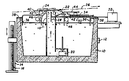
A solder reservoir 10 is shown in Figure 1 supported
by a support frame 12 which in turn is connected to a
screw jack 14 having a screw 16 that can be rotated to
lower and then raise the solder reservoir 10. The
reservoir 10 is shown in the position for wave soldering,
and can be lowered for maintenance purposes.
In the solder reservoir 10 a solder nozzle 18
extends up above the solder level and a pump 20 pumps
solder up through nozzle 18 to form a solder wave 22.
The solder wave 22 illustrated is similar to that shown
in U.S. Patent 3,921,888 to Elliott et al and provides a
smooth l~inAr flow solder wave 22 which is non-
turbulent. An element 24 such as a printed circuit boardis shown passing in a conveyor path 26 so that at least a
portion of the board 24 passes through the solder wave
22. In some cases the solder wave is arranged to only
contact the underside of the board 24, however, the
height of the solder wave can be adjusted by varying the
pump flow and/or by raising and lowering the reservoir 10
to suit the different soldering requirements.
A vibrator plate 28 in the nozzle 18 is attached to
a rod 30 connecting to a vibr~ or 32 to provide an
oscillation or vibration to the solder wave 22 during the
passage of a printed wiring board therethrough. The
vibratory arrangement is disclosed in U.S. Patent
4,684,056 to Deambrosio. The oscillation or vibration
aids in filling or wicking up into small holes in the
~ ~o 93/1 16~ 2 1 2 5 0 ~ O PCr/CA92/00~
-- 10 --
boards. Crevices and corners adjacent to a solder mask
are also solder wetted, as well as all other areas where
solder wetting is difficult to achieve by co~ventional
machines.
A cover plate 34 is shown over the top of the solder
reservoir 10, and has skirts 36 which extend around the
perimeter of the plate and extend down into the solder in
the reservoir 10 to provide a seal thus providing a
contained space under the cover plate 34. Brackets 38
support the cover plate 34 on the sides of the reservoir
10. The cover plate 34 has a longitudinal slot 40 which
extends along the solder wave and provides an aperture
through which the solder wave projects. Lips 42 are
shown around the edges of the slot 40 to provide a curved
edge. The lips 42 are not always necessary as will be
seen in the later drawings. On the downstream side of
the solder wave 22, a sliding damper plate 44 is provided
to reduce the size of the gap adjacent the downstream
side of the solder wave 22. In certain solder waves, the
slot 40 extends around the ends as well as the sides. A
supply of gas may be supplied if necessary to ensure that
the slot at the ends has gas flowing out to blanket the
ends as well as the sides of the solder wave.
Gas pipes 46 are shown positioned on each side of
the solder wave 24 under the cover plate 34. The gas
pipes 46 may be gas diffusers or, alternatively, may be
pipes with holes therein. They are positioned as close
to the solder wave as possible and in some instances the
solder may touch or even flow over the gas pipes 46. Gas
is supplied to the gas pipes 46 and the gas flows upwards
through the slot 42 on each side of the solder wave 22,
thus enveloping or blanketing the solder wave 22. When a
circuit board 24 passes through the solder wave, the
board forms a reaction wall and the gas not only covers
the solder wave but also provides a canopy which
_ WO 93/1 16~ 2 12 5 0 4 0 PCl /CA92/OO~
-- 11 --
surrounds the circuit board 24 or element passing through
the solder wave. In this manner the gas atmosphere
blankets not only the surface of the reservoir within the
cover plate 34 but also blankets the surface of the
solder wave and provides a canopy over circuit boards or
other elements passing through the solder wave 22.
The type of gas used to blanket the solder wave may
be an inert gas such a nitrogen, a shield gas, a
treatment gas, or reducing gas may be used. In all cases
oxygen is excluded to achieve reliable soldering, and
preferably to the smallest amount possible. The gas may
include additives which are desirable for solder coating
of wettabie metallic surfaces or for joining at least two
wettable metallic surfaces.
Low dross solder contains a phosphorous
concentration generally in the range of about 10 to 1000
ppm. One example of a low dross solder is sold by Alpha
Metals under their tradename HI FLO Alloy 63/37. When
this solder is used in an atmosphere with a reduced
oxygen content, then it is found that solder bridging and
excessive solder deposits on metallized surfaces no
longer occurs, or at least is reduced. Furthermore,
whereas in the past in order to attain reduction in
solder dross, it was necessary to have a pure nitrogen
atmosphere. This is no longer required and oxygen
contents of up to 10,000 ppm (5%) are satisfactory for
reduction in dross, furthermore bridging and excessive
solder deposits are eliminated or at least reduced. When
oxygen is reduced to 5% or less in a shield gas, dross
formation is reduced even utilizing the low dross solder.
Thus use of low dross solder eliminates the need to inert
the solder waves with a high purity nitrogen or a more
expensive inert gas such as argon. By using nitrogen or
another inert gas with a higher oxygen content, one
reduces the cost of the gas. Pure nitrogen is expensive
212SO~O
_ WO93/116~ rcT/cAs2/
- 12 -
whereas a lower purity of nitrogen is far cheaper.
Nitrogen can be produced from air using membrane
technology. Such a process retains some oxygen content
but generally less than lO,000 ppm (5%) which is
satisfactory for use with the present invention. The
oxygen content of the Rhield gas, primarily nitrogen is
preferably in the range of l to 50,000 ppm (5%) and in a
specific preferred embodiment lO to l,000 ppm.
Whereas Figure l illustrates a non-turbulent solder
wave, other types of solder waves may be used. For
instance, a uni-directional hollow jet wave flowing
either with or counter to the direction of movement of
the conveyor in the conveyor path 26 may be provided.
Single or multiple solder waves can be covered in the
manner disclosed herein. There may be two waves of the
same type or different types, such as turbulent, non-
turbulent, lA~inAr flow, hollow waves, but not limited to
these types. Figure 2 shows another embodiment with two
solder waves, a first turbulent solder wave 50, followed
by a non-turbulent smooth 1A~; n~r flow solder wave 22 of
the type shown in Figure l. In the embodiment of Figure
2, two slots 40 are provided for the two solder waves 22
and 50. The conveyor path 26 for the circuit boards 24
is shown inclined however in other embodiments the
conveyor path may be horizontal as is illustrated in
Figure 3. Beneath the cover plate 34, gas pipes 46 are
shown on both sides of the two solder waves 22 and 50.
Baffles 52 are provided underneath the gas pipes 46 to
ensure that a majority of the gas is directed to flow
through the slots 40 adjacent the solder waves 22 and 50
to blanket the solder waves. Whereas gas pipes 46 are
shown on both sides of the solder wave, in another
embodiment gas is supplied directly to the space under
the cover plate in a sufficient quantity to ensure that
no air remains in the space and gas passes out of the
slot 40 on both sides of the solder wave.
2125~40
_ ~093/ll6~ rcT/cAs2/
- 13 -
Figure 3 shows another embodiment wherein a hood,
enclosure or tunnel 54 is provided to contain a
horizontal conveyor path 26. Curtains 56, either gas
curtains or flaps, are shown at the entrance and exit to
S the tunnel 54 and heaters 58 are provided to preheat
elements that pass along the conveyor path 26 within the
tunnel 54. Whereas the conveyor path 26 is shown as
being horizontal, it may be inclined upwards in the
direction of travel. The tunnel or hood 54 may contain
an inert gas atmosphere or a shield gas atmosphere that
excludes oxygen which may or may not be different to that
provided under the cover plate 34 above the solder in the
reservoir 10. The solder pipes 46 still provide a gas to
blanket the solder waves 22 and 50 and react with boards
24 passing through the solder waves. Heaters 58 are
shown in Figure 3 to illustrate that a preheat may occur
within an enclosed and controlled atmosphere. In another
embodiment, a fluxer may be included prior to soldering,
or other treatment may be applied to the boards prior to
soldering.
Figure 4 illustrates an embodiment wherein gas knife
jets 60 are shown positioned on both sides of a solder
wave 22 directed to produce a jet or line of gas towards
the slot 40 on each side of the solder wave 22. The
cover 34 is shown having a seal 61 to the top side of the
reservoir 10. In this embodiment, no skirt 36, as shown
in Figures 1, 2 and 3 is provided, instead the cover 34
seals to the rim of the reservoir 10. In the case of a
tunnel 54 as shown in Figure 3 over a solder reservoir,
the skirts 36 may be replaced with seals 62 around the
rim of the reservoir 10.
Figure 5 illustrates another embodiment wherein a
shroud 62 is shown surrounding a solder wave 22. The
term "shroud" used herein is to distinguish the article
from a cover. The shroud generally surrounds the solder
~ W093/116~ 2125 04 D PCTtCA92/~o~t
- 14 -
wave and the area in the solder reservoir adjacent to it.
A shroud i8 a type of cover in the present text. Gas
diffusers or gas pipes 46 provide gas within the shroud
62 which has skirts extending down below the level of
solder in the reservoir 10. The gas flows upwards in the
slot 40 on each side of the solder wave to blanket the
solder wave. If gaps are provided between the shroud 62
and the ends of the solder wave, then gas flows from
these gaps.
Figures 6 and 7 illustrate a cover plate suitable
for a solder machine having two solder waves therein.
The cover plate 34 has skirts 36 extending around all
four sides and has two slots 40 for the solder waves to
pass therethrough with a perimeter bead 64 extending
around the peripheral outside edges of the slots, but not
the inside edges. The cover plate is separate from but
mates with a tray 66 having side plates 68 extending
upwards at both ends. The side plates 68 have slots 70
therein for attachment for example to a conveyor support
frame (not shown) of a soldering machine. The slots 70
allow limited vertical movement of the tray 66 and hence
the cover plate 34 thus takes into account height
adjustment of the solder reservoir 10 when required. The
tray 66 remains in position attached to the conveyor
support frame when the solder reservoir 10 with cover
plate 34 thereon is lowered for maintenance purposes.
The bead 64 acts as a guide to position the cover plate
34 so that it mates to the tray 66 when the solder
reservoir 10 is raised up to a soldering position.
The gas pipes 46 are shown each having individual
valves 72 so that the flow of gas can be controlled to
each individual pipe. The gas is supplied through a
manifold 74 for feeding to the pipes.
_,~093/ll6~ 212 ~ O ~ O pcT/cAs2/ons~
- 15 -
Figure 8 illustrates another emboA;~e~t of a cover
plate wherein a first intermediate skirt 76 is shown
between the two gas pipes 46 beneath the strip between
the two slots 40. A further intermediate skirt 78 is
shown adjacent the gas pipe 46 on the downstream side of
the second solder wave and the cover plate 34 between the
intermediate skirt 78 and the end skirt 36 has a series
of holes 80 therein which extend into a channel 82 formed
by a top plate 84 attached to the perimeter bead 64. The
channel 82 directs gas to flow substantially horizontally
towards the downstream solder wave to provide a jet or
stream of gas. Thus two c~s flows are provided, one
through the gas pipe 46 directly on the side of the
solder wave and the other through the channel 82. By
providing the substantially horizontal flow of gas,
improved blanketing of certain gas waves is achieved. By
utilizing valves 72 to the gas supply for individual gas
pipes 46 different flows of gas can be arranged through
the different slots on both sides of the solder waves
thus ensuring that satisfactory blanketing of the solder
wave and reaction with the board passing through the
solder wave is attained.
Another embodiment is shown in Figure 8A, s;~;lar to
that shown in Figure 8, wherein the top plate 84 is
raised up providing a wider channel 82 and the gas is
then able to flow in both directions. It has been found
that when the gas flows only in one direction as shown in
Figure 8, air which is entrained along the bottom surface
of the top plate 84 is drawn into the jet or stream of
gas. By providing for the gas to escape in both
directions along the channel 82, less air is drawn i~to
the stream of gas applied to the solder stream. This
reduces air substantially around the solder wave and
results in clean oxide free soldering.
212~040
_ ~09~/ll6~ PCT/CA92/00
- 16 -
Two hollow solder waves 90 are shown in Figure 9
directed towards each other from hollow wave nozzles 92
fitted into chimneys 94. The nozzles 92 are replaceable
to permit different nozzles having different angles of
projection, and different sized jets. The jets may be a
plurality of round holes in a row, or may be a slit.
A cover plate 34 extends over the surface of the
solder reservoir, and has skirts 36 extending down into
the solder. Two slots 40 are provided in the cover plate
34 for the two hollow solder waves 90. In another
embodiment the center cover skirts between the two slots
may be considered as a second cover. Sliding damper
plates 44 with sloped flanges 96 are positioned adjacent
the sides of the slots, and machine screws 98 are
provided to clamp the damper plates 44 in place. The
damper plates 44 can be positioned to just clear the
solder waves 90 and can be adjusted for different flows
and angles of solder wave.
Gas pipes 46, preferably gas diffusers, are
positioned below the cover plate 34 on each side of the
solder waves 90. In another embodiment, although not
always required, gas pipes 46A are placed underneath the
solder waves so that gas blankets all sides of the solder
wave. A divider sheet 100 is positioned in between the
solder waves 90 extending up to the cover plate 34. Gas
pipes 46 are placed on each side of the divider sheet 100
so that different gas flows can be applied to each solder
wave.
Another embodiment of cover plate 34 for a single
hollow solder wave 90 is shown in Figure 10. The cover
plate has sloped lips or flanges 102 which extend to a
complete cover 104 at each end of the solder wave. Thus
the slot 40 is cut from the cover plate 34 without having
damper plates 44. A separate curved cover 106 is
_~093/116~ - 17 - pcT/cAs2/~n~
provided over the gas pipe 46A under the ~older wave 90.
This curved cover 106 ensures the gas is deflected to the
exposed surfaces of the solder reservoir and the
undersurface of the solder wave.
The solder wave 22 of Figure 1 is similar to that
shown in U.S. Patent 3,921,888 to Elliott, and in the
embodiment shown in Figure 11, a separate diffuser
arrangement 110 is located above the cover plate 34,
downstream of the solder wave 22. The diffuser
arrangement has three diffusers 112 therein and a series
of substantially parallel flat vanes 114 which extend
from a surrounding housing 116. Inert gas, preferably
nitrogen, is expelled from the diffusers 112 and flows
along the vanes 114 to produce a 1A~; nAr flow of gas
which is entrained by the gas exiting from under the
cover plate 34. The vanes 114 are shown to be
substantially horizontal and the conveyor path 26 sloped
upwards. In another emboAiment the conveyor path 26 is
horizontal, and the vanes 114 are arranged either
horizontally or sloping to ensure that there is lAmi n~r
flow from the diffuser arrangement 110 to entrain with
the laminar flow of gas from under the cover plate 34 and
blanket the solder wave with a lAm; n~r flow of gas.
Elements, preferably circuit boards 24, are shown in
Figure 12 being conveyed substantially horizontally on a
conveyor 26 through a fluxer 118 for applying a flux to
the wettable metallized surfaces to be coated or joined.
The flux may be a no-clean flux which is a flux that
after solder coating leaves a low level of residue that
is both non-corrosive and non-conductive. This avoids
the necessity of having to clean the flux residues off
the surfaces after soldering. In some cases other types
of flux are used and a solvent cleaner may be applied to
clean the flux off the solder coated surfaces after the
soldering step. One type of no-clean flux includes
21250~0
~093/116~ PCT/CA92/00
- 18 -
adipic acid, up to 3% by weight. Other types of no-clean
flux are readily available on the market today.
After the fluxing step, which is only necessary in
certain types of soldering under reduced oxygen
environments, the elements 24 on the conveyor 26 pass
through a heating stage. Preheaters 120 heat the
elements 24 up to the required temperature for soldering.
In one embodiment the preheating and fluxing stage occur
in air, however in other embodiments both the preheating
and the fluxing stage either individually or together may
occur within a shield gas environment with reduced oxygen
to prevent oxidizing of surfaces to be soldered.
A solder reservoir 10 has solder therein, the solder
in one embodiment is a low dross solder, however, in
other instances shield gases may permit the use of
conventional solders without dross forming. Two solder
waves 22A and 22B are shown, one after the other, both
solder waves 22A and 22B illustrated are turbulent waves
wherein solder is pumped by an additional pump 20 up
through a nozzle 18. The solder pumps 20 are adjustable
to permit adjustment of the heights of the solder waves
22A and 22B.
Two turbulent solder waves shown in Figure 12 are
small waves from narrow nozzles and easy to control. The
two pumps 20 can be varied to control the height of the
solder waves 22A and 22B for different types of elements
24 to be soldered. The height of the elements 24 above
the solder waves 22A and 22B can also be adjusted by
positioning the elements 24 at a desired elevation on the
conveyor 26.
Shrouds 34, or cover plates similar to those
disclosed in the previous figures, are provided over the
solder reservoir 10 leaving slots 40 for the solder waves
_~093/1l6~ 212 ~ O ~ O PCT/CA92/00~'~
-- 19 --
to exit. The slots 40 leave gaps between the edge of the
slot 40 and the solder wave 22A or 22B and gas diffusers
46 are positioned on each side of the solder wave below
the shroud 34 so that the space under the shroud and
above the solder level in the reservoir 10 is completely
blanketed with shield gas. The gaps provide a sufficient
flow of shield gas to cover or blanket the side of the
solder wave, and at the same time prevent air from
entering the shroud. The size of the gaps are preferably
not wider than necessary to keep the shield gas flow as
low as possible, and still provide the necessary
blanketing. There is an escape of gas through the slots
40 in the gaps on both sides of the solder waves 22A and
22B. The gas is shield gas and preferably has less than
5~ oxygen. In a preferred embodiment gas is nitrogen and
blankets solder in the solder reservoir 10 and also
blankets both sides of the solder wave when an element 24
is passing through the wave.
The shroud 34 has skirts 36 on all sides extending
down into the solder in the solder reservoir 10. A
divider skirt 100 in the center of the shroud 34 also
extends down into the solder wave, thus providing two
separate spaces, one for each solder wave. This permits
the flow of gas into the two spaces to be controlled
separately. In one case a higher pressure may be desired
or greater flow may be desired in one of the spaces.
After the elements or boards 24 pass through the
solder waves 22A and 22B, a gas knife 122, preferably of
the type shown in U.S. patent 4,679,720 or 4,995,411,
provides a linear jet of gas which is directed against
the underside of the element 24 and blows off any excess
solder. The gas knife may be heated or, alternatively,
gas entering the gas knife may be heated. Furthermore
the position of the gas knife 122 can be varied
vertically and horizontally, the knife may be rotated so
2125010
_ WO9~/116~t PCTtCA92/0
- 20 -
the gas projects at different angles. This permits
adjustments to be made for different types and sizes of
elements 24 and boards. The gas may be a shield gas with
reduced oxygen or, alternatively, may be air.
Figure 13 shows another embodiment wherein the
conveyor 26 is sloped upwards. Different types of solder
waves 22A and 22B are illustrated wherein a first solder
wave 22A is a turbulent solder wave and the second one
22B is a non-turbulent smooth 1A~; nAr flow solder wave of
the type shown in U.S. patent 3,921,888.
One, two or more solder waves may be provided, the
solder waves may be of all wave configurations including
turbulent, streamline, hollow jet and combinations of
different configurations. The list of configurations is
in no way limiting.
The gas knife 122 is shown mounted on the shroud 34
after the second solder wave 22B, projecting upwards to
ensure that a linear jet blows against the underside of
the element as it passes. Solder blown of f the element
may be arranged to return to the solder reservoir.
The shroud 34 together with the gas knife 122 may
f orm part of a retro package f or installation on existing
solder wave equipment. The shroud 34 is made to fit over
the solder reservoir 10 and the elongated slots 40 are
provided to fit the solder wave or solder waves. Whereas
two solder waves are shown in the drawings, more than two
solder waves may be used if required or, alternatively a
single solder wave may also be used.
An enclosure 124 or tunnel is shown in Figure 14
enclosing the conveyor 26 as elements or boards 24 are
conveyed past the fluxer 118 and the preheaters 120. An
entrance curtain 126 and an exit curtain 128 are provided
_ ~093/116~ 212 5 0 4 0 PCT/CA92/005'~
- 21 -
to restrict gas from escaping from the enclosure 124. A
shield gas environment may be maintained within the
enclosure 124. Figure 15 shows an enclosure 130, or hood
positioned over the solder pot 10 only without a gas
knife, and Figure 16 shows an extended tunnel 132
extending over the conveyor 26 from the fluxer 114, the
preheaters 120 and the solder reservoir 10. The
enclosure 132 also extends over a gas knife 122
positioned directly after the solder reservoir 10.
A different solder nozzle arrangement 18 is shown in
Figure 17 with guides 134 on both sides of the nozzle.
The solder wave has a smooth streamline flow falling back
on both inlet and exit of the nozzle 18 and guided back
into the solder reservoir by the guides 134. This type
of solder wave is sometimes defined as a bi-directional
solder wave.
Adjustable strips 136 are mounted on the shroud 34
adjacent the slots 40 to permit the gaps to be varied for
different wave heights. Provision is also made in one
embodiment to raise or lower either the conveyor or the
solder pot so the height between the solder wave and the
conveyor line 26 can be varied.
The diffusers 46 for shield gas supply, preferably
nitrogen, may be replaced with drilled tubes. The shield
gas supply can be turned off with the solder wave when no
boards are present as the shield effect is almost
instantaneous. Intermittent use of shield gas reduces
gas consumption.
Figure 18 shows a solder wave arrangement with a
turbulent first solder wave 22A and a smooth streamline
bi-directional second solder wave 22B similar to that
shown in Figure 17. The conveyor line 26 is shown sloped
but in another embodiment may be substantially
~ W093/ll6~ 212 5 0 ~ O PCT/CA92/00~'~
- 22 -
horizontal. A vibration blade 138 attached by a rod 140
to a vibrator 142 provides a vibration to the wave in
accordance with U.S. patent 4,684,056 (Reissue patent Re
33,197)-
The bi-directional solder wave 22B has a smooth top
solder surface. When an element or board 24 passes
through the solder wave 22B the shield gas passes through
the gaps on each side of the wave and shields or inerts
the space between the solder wave 22B, the shroud 34 and
the board 24.
The embodiment shown in Figure 17 has the shroud 34
attached to the side of the solder reservoir 10 while in
the embodiment shown in Figure 18, the shroud 34 has
skirts 36 extending down into the solder to provide a
seal and ensure the space under the shroud can be sealed
to prevent entry of air into the shielded atmosphere.
In Figure 19, an enclosure 132 is provided over the
solder reservoir 10 which is sealed to the top edge of
the solder reservoir 10. The enclosure 132 or tunnel
contains shield gas that passes up through slots 40 from
under the shrouds 34A and 34B. In the embodiment shown,
a first shroud 34A surrounds the first solder wave 22A
and a second shroud 34B surrounds the second solder wave
22B. The separate shrouds permit individual shield gas
supply. The shroud top surfaces are flat to trap shield
gas within.
Figure 20 shows a bi-directional solder wave 22 with
a gas knife 122 positioned on the exit side of the wave
22 under the shroud 34 to direct gas through the slot 40
to blanket the wave. When a board 24 is passing through
the wave the gas knife diverts gas, either shield gas, or
in certain cases air, to blanket the space where the
board leaves the solder wave. This protects the board
-_ ~093/ 1165~ 2 12 5 0 ~ O P~T/CA92/~05~.
- 23 -
with the fresh solder surfaces thereon and the solder
wave.
Whereas Figure 19 shows an enclosure 132 over two
solder waves, in Figure 21 two separate top covers 144
5 are provided over the shrouds 34A and 34B and solder
waves 22A and 22B, the top covers 144 not extending for
the full lengths of the shrouds 34A and 34B. The top
covers 144 help to trap shield gas passing up through the
slots 40 and thus reduce oxide formation on the crest of
the solder waves. The top of the top covers 144 are
preferably glass for viewing the wave and the sides 146
are adjustable for height and are made from flexible
material to act as curtains. The sides 146 may be pushed
aside when circuit boards are conveyed on the conveyor
15 path 26.
The conveyor path is shown inclined upwards but in
another embodiment is substantially horizontal. The
second solder wave 22B is a bi-directional wave, the
nozzle 18 with the plates 134 is adjustable vertically to
20 adjust wave height. Wave flow is adjustable by means of
the solder pump 20. With a combination of varying wave
height and wave flow, the inclination of the conveyor
path 26 is also ad~ustable.
In the embodiment shown in Figure 22, the circuit
25 board 24 is supported on fingers 150 from the conveyor
26. A gas knife 122 is positioned on the exit side of
the wave 22B and may be pivoted to adjust the direction
of gas flow from the gas knife 122. A rubber seal flap
152 is connected to the side of the shroud 34B extending
30 down to the skirt 36 in the solder reservoir. The seal
flap is made of suitable material that is flexible, so
the gas knife may be pivoted to a preferred location to
selectively direct gas, and prevents gas exiting from
under the shroud 34B downstream of the gas knife 122.
WO 93/116~3 212 5 0 4 0 PC'r/CA92/00~'3
-
- 24 -
Various changes may be made to the embodiments shown
herein without departing from the scope of the present
invention which is limited only by the following claims.