Note: Descriptions are shown in the official language in which they were submitted.
D/91393 212~0S2
AN INTEGRATED DEVICE HAVING MOS TRANSISTORS WHICH ENABLE POSITIVE AND
NEGATIVE VOLTAGE SWINGS
It is an object of this invention to provide a technique for realizing large
negative and positive voltage swings with respect to p-type and n-type substrates by
utilizing metal oxide silicon field-effect (MOSFET) transistors integrated with
complementary-symmetry metal oxide silicon field-effect (CMOS) circuits. This
invention is capable of generating voltage swings as low as -60V and as high as
+ 60V. This invention can utilize p-channel MOSFET (PMOS) transistors or n-channel
type MOSFET (NMOS) transistors to provide a design for a negative and positive
voltage swing circuit. Also, this invention eliminates the need for using bulky
discrete elements used in the design of the prior art negative voltage swing circuits.
BRIEF DESCRIPTION OF THE DRAWINGS
Other objects will become apparent from the following description with
reference to the drawings wherein:
Figure 1 shows a circuit diagram of a prior RS232 driver made with a
discrete resistor;
Figure 2 shows a curve of a prior art voltage swing between a positive
voltage and a negative voltage;
Figure 3 shows a structure of a prior art p-channel metal oxide silicon field
effect transistor (PMOS) fabricated on a p-substrate;
Figure 4 shows an integrated circuit diagram of a RS232 driver of this
invention utilizing two PMOS transistors;
Figure 5 shows the structure of the circuit of Figure 4 utilizing two low
voltage transistors;
Figure 6 shows the structure of the circuit of Figure 4 utilizing two high
voltage transistors;
Figure 6A showsthe structure of the circuit of Figure 4 utilizing two high
voltage transistors with two n-well areas designed to handle high voltages;
Figure 7 shows a curve of a voltage swing of this invention which swings
between a ground potential and a negative voltage;
Figure 8 shows a curve of a voltage swing of this invention which swings
between a positive voltage and a negative voltage;
Figure 9 shows the circuit diagram of Figure 4 in conjunction with a level
translator;
2 1 25052
Figure 10 shows a curve of an input voltage swing;
Figure 1 1 shows a curve of the input voltage swing of Figure 10 after it has been
shifted;
Figure 12 shows a circuit diagram of a power normal application of this invention;
Figure 13 showsacurveofthevoltageofnode 1400fFigure 12;
Figure 14showsacurveofthevoltageofnode 1420fFigure 12;
Figure 15 shows an integrated circuit diagram of a RS232 driver of this invention
tili7ing two NMOS transistors; and
Figure 16 shows the structure of the circuit of Figure 15 lltili7in~; two low voltage
1 o transistors.
SUMMARY OF THE INVENTION
It is an object of an aspect of this invention to provide a way to design a circuit for
generating large negative and positive voltage swings with respect to p-type and n-type
substrates. It is an object of an aspect of this invention to integrate the negative and
positive voltage swing circuit of this invention with CMOS circuits and therefore
elimin~te the need for the discrete elements used in the negative voltage swing circuits.
This invention is based on elimin:~tion of the output electro-static discharge (ESD)
2 o protection circuit which has been a commonly accepted requirement for any integrated
circuit. Flimin~ting the ESD protection circuit also elimin~tes the clamping feature of the
ESD protection circuit and therefore the output of the integrated circuit can be connected
to negative voltages. This permits the use of an on chip integrated circuit to generate a
negative voltage swing.
Other aspects of this invention are as follows:
In a high voltage system comprising:
an integrated device having a p-type substrate, a plurality of p-channel type metal
3 o oxide silicon field-effect transistors, a plurality of n-channel type metal oxide silicon field-
effect transistors;
21 25052
said p-channel type metal oxide silicon field-effect transistors and said n-channel
type metal oxide silicon field-effect transistors each having a source, a drain and a gate;
at least one of said p-channel type metal oxide silicon field-effect transistors being
an output transistor;
said system including a ground potential, a voltage source above said ground
potential and a voltage source below said ground potential;
said substrate being connected to said ground potential; and
said drain of at least one output transistor being connected to said voltage source
below said ground potential and said source of said at least one of said output transistor
being connected to said voltage source above said ground potential.
In a high voltage system comprising:
an integrated device having a n-type substrate, a plurality of n-channel type metal
oxide silicon field-effect transistors, a plurality of p-channel type metal oxide silicon field-
effect transistors;
said n-channel type metal oxide silicon field-effect transistors, and said p-channel
type metal oxide silicon field-effect transistors each having a source, a drain and a gate;
at least one of said n-channel type metal oxide silicon field-effect transistors being
an output transistor;
2 o said system including a positive voltage source, a voltage source above said
positive voltage source and a voltage source below said positive voltage source;said substrate being connected to said positive voltage source; and
said drain of at least one output transistor being connected to said voltage source
above said positive voltage source and said source of said at least one of said output
2 5 transistor being connected to said voltage source below said positive voltage source.
DESCRIPTION OF THE PREFERRED EMBODIMENT
Typically a negative voltage swing circuit is made with discrete components.
3 o Referring to Figure 1, there is shown a circuit diagram of a prior art RS232 driver 10
which is capable of providing a negative voltage swing. This circuit is made of a discrete
PMOS transistor 12 and a discrete resistor 14. In this circuit the source 16 of the PMOS
2l 25052
transistor 12 is connected to a positive voltage + Vss, the drain 18 is connected to a
negative voltage - VDD through the resistor 14 and the gate 20 is connected to an input
voltage Vi which swings between 0 to + 5V. The output voltage VO is the voltage of the
drain 18 ofthe PMOS transistor 12.
2b
D/91 393
212~0S2
In operation, when the input voltage Vj is in the neighborhood of the
ground potential, the PMOS transistor 12 is ON. When the PMOS transistor 12 is ON,
the output voltage approximately becomes + Vss. However, when the input voltage
Vj is at + 5V, the PMOS transistor 12 is OFF and as a result, the output voltage drops
to a voltage close to VDD. Therefore, the output voltage VO of this circuit swings
approximately between +Vss and VDD. Referring to Figure 2, there is shown an
example of a voltage swing between + Vss and VDD. The horizontal axis representstime and the vertical axis represents voltage.
Usually, the circuit shown in Figure 1 does not require an electro-static
discharge (ESD) protection circuit since a discrete transistor is large enough to
withstand an ESD shock. However, if the same circuit 10 is built in an integrated
circuit, due to the commonly accepted practice of designing elements of an
integrated circuit with the smallest layout area, an output ESD protection circuit is
required on the output transistor to prevent the transistor from destruction. Itshould be noted that an output transistor is a transistor that is connected to
elements outside of the integrated circuit and it is the output transistor that requires
an ESD protection. An output ESD protection circuit clamps down any negative
voltages applied to the circuit. Therefore, due to the clamping feature of the output
ESD protection, it has been a commonly accepted principle that an integrated circuit
can not be used to generate a negative voltage swing.
This invention ignores the commonly accepted principle that integrated
circuits cannot be used to generate negative voltages by going contrary to the
commonly accepted practice of designing elements of an integrated circuit with the
smallest area and increasing the layout area of a transistor to handle an ESD shock
and therefore eliminate the previously required ESD protection circuit. This change
permits an output transistor to withstand an ESD shock without an ESD protectioncircuit and also permits an integrated circuit to be used for negative voltage swing
applications. It should be noted that the size of the transistor depends on manydifferent factors such current, sourcing/sinking, speed of response, etc.
In order to apprehend this invention, it is necessary to study the structure
of an integrated MOS transistor fabricated with complementary-symmetry (CMOS)
circuits in a single tub bulk CMOS technology.
D/91393
212~0S2
Referring to Figure 3, there is shown a structure of a p-channel type metal
oxide silicon field effect transistor (PMOS) 30 fabricated on a p-type substrate 32.
The PMOS transistor on a p-type substrate consists of a n-type well or tub 34, two
p + regions within the n-well 34 to function as the source 36 and the drain 38 of the
transistor. A metal/poly gate 40 is located above the n-well 34. However, the gate
40 is insulated from the n-well 34 by a layer 42 such as silicon dioxide.
Typically, in a structure such as PMOS transistor 30, the p-substrate 32 is
connected to the most negative voltage on the chip which is the ground potential,
the n-well 34 is connected to the source voltage or to the most positive voltage on
the chip, i.e. + 5V, and finally the gate 40 is connected to a positive voltage in the
range of 0V to + 5V. Usually, if the transistor 30 is an output transistor an ESD
protection circuit is required to protect the transistor from the ESD shocks. A
conventional output ESD protection circuit comprises a n + diode which typically is
placed between the drain and the substrate. The n + diode forward biases when the
voltage of the drain is 0.7V below the substrate. In the past, due to the clamping
feature of the ESD protection circuits, it has been common knowledge that the drain
38 can not be connected to voltages lower than the voltage of the p-substrate 32which is the ground potential.
However, by eliminating the ESD protection circuit, the drain 38 can in
fact be connected to negative voltages (below the substrate voltage which is at the
ground potential) as long as the difference between the drain voltage and the
ground potential is kept below the breakdown voltage of the transistor. When then-well 34 is connected to a positive voltage + Vn, the drain 38 can be connected to a
negative voltage VDD as long as the difference between the voltage of the n-welland the drain voltage is kept below the breakdown voltage [ VBR > ( + Vn) - (- VDD)1
Being able to connect the drain of a PMOS transistor to negative voltages
(below the substrate voltage), provides a way to achieve negative voltage swingswhich is a desirable feature that can be utilized in many different applications such
as drivers for RS232 interface, phase array radar drivers and power normal circuits.
It should be noted that the same applies to an NMOS in a n-type substrate
only with opposite polarities. Meaning that in an integrated circuit with a n-type
D/91393
2125052
substrate, if the ESD protection is eliminated, the drain of a NMOS transistor can be
connected to voltages above the substrate voltage.
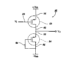
Referring to Figure 4, there is shown a PMOS negative and positive
voltage swing circuit 50 which can be integrated with CMOS circuits. In this
invention the discrete transistor 12 (Figure 1) and the discrete resistor 14 (Figure 1)
are replaced by two PMOS transistors 52 and 54. In this circuit the source 56 of the
PMOS transistor 52 is connected to a positive voltage + Vss, the gate 58 of the PMOS
transistor 52 is connected to the input voltage Vj and the drain 60 of the PMOS
transistor 52 is connected to the source 62 of the PMOS transistor 54. In order to
have the transistor 54 function as an active resistor, its gate 64 is connected to its
drain 66 and the drain 66 is connected to a negative voltage VDD. BY connecting the
gate 64 of the PMOS transistor 54 to its drain 66, the PMOS transistor 54 acts as an
active resistor.
Referring to Figure 5, there is shown a structure of the circuit 50 of Figure
4 utilizing two low voltage PMOS transistors. The two p + regions 56 and 60 of the
PMOS transistor 52 and the two p + regions 66 and 62 of the PMOS transistor 54 are
diffused into n-wells 72 and 74 respectively to generate the sources 56 and 62 and
the drains 60 and 66. Metal/poly gates 58 and 64 are insulated from the n-wells by
two layers of silicon dioxide 76 and 78 respectively. The substrate 70 is connected to
the ground potential through the P + region 80. It should be noted that the n-well
72 of PMOS transistor 52 and the n-well 74 of PMOS transistor 54 have to be
connected to the same potential or both transistors 52 and 54 have to be in the same
n-well. The n-well 72 and the n-well 74 are connected to the most positive voltage
through the n + regions 82 and 84 respectively.
Referring to Figure 6, there is shown a structure of the circuit 50 (Figure 4)
utilizing two high voltage PMOS transistors. It should be noted that all of the
process steps for deposition of materials, etching and patterning of the transistors
shown in Figures 5, 6 and 6A are well known in the art. In Figure 6, for the purpose
of simplicity and in order to be able to refer to Figures 4 and 9, the two PMOS
transistors, the source regions, the drain regions, the gates, the n-wells and the
substrate are all given the same reference numbers used in the structure of the
circuit 50 utilizing low voltage transistors (Figure 5).
D/91393
212S052
In the structure shown in Figure 6, layers of field oxide 92 and 94 are
located adjacent to the source regions 56 and 62. There is also a layer of field oxide
96 located between the drain 66 and the n + region 84 and another layer of fieldoxide 96 located between drain 60 and the n + region 82. P- type offset regions 90
are located under layers of field oxide 92, 94 and 96. The gates 58 and 64 are
insulated from the n-wells 72 and 74 by two layers 76 and 78 of silicon dioxide
respectively. The offset regions 90 have lower impurity concentration than the
impurity concentration of the source regions 56 and 62 in order to have high
resistance. The offset regions 90 redistribute the electric field density created due to
the high voltage thus increasing the breakdown voltages of regions 56 and 62.
In operation of the embodiment of Figures 4, 5 and 6, when the input
voltage Vj is in the neighborhood of the ground potential, the PMOS transistors 52
and 54 are ON. When the PMOS transistors 52 and 54 are ON, the output voltage
becomes approximately + Vss. However, when the input voltage Vj is at + 5V, the
PMOS transistor 52 is OFF and therefore the output voltage drops to a voltage close
to VDD-
When the n-wells 72 and 74 are grounded, the output VO swings between
the ground potential and VDD as long as the difference between ground and
VDD jS not more than the breakdown voltage. For example, with high voltage
transistors (Figure 6), if the breakdown voltage is 60V and VDD jS -60V, then the
output VO swings between 0V and -60V. Referring to Figure 7, there is shown an
example of a voltage swing between 0 and -60. The horizontal axis represents time
and the vertical axis represents voltage. It should be noted that for a high
breakdown voltage such as 60V the structure of Figure 6 will be used. However, if a
low voltage swing is needed, the structure of Figure 5 can provide a negative voltage
swing in the range of its breakdown voltage.
Referring back to Figure 4, circuit 50 of this invention is capable of not
only generating negative voltage swings but also positive voltage swings. In Figures
5 and 6, when the n-wells 72 and 74 are connected to a positive potential such as the
source voltage +Vss with respect to the grounded substrate 70, as long as the
difference between + Vss and VDD jS less than the breakdown voltage, the output
VO swings between +Vss and VDD. For example, with high voltage transistors
(Figure 6), if + Vss is + 5V and the breakdown voltage VBR jS 60V, then VDD can not
D/91393
212~052
be more negative than -55V and therefore the output voltage VO swings between
+ 5V and -55V. It should be noted that in the structure of Figure 6, the PMOS
transistors 52 and 54 are high voltage transistors and they have a high breakdown
voltage. However, the n-wells 72 and 74 are not designed to be connected to highvoltages. Therefore, the n-wells 72 and 74 can handle a voltage in the range of 0 to
+ 5 V. Circuit 50, with the structure of Figure 6, has a negative voltage swing as low
as -60V and a positive voltage swing as high as + 5V. However, if a positive voltage
swing with a higher voltage is desired, the n-wells 72 and 74 can be designed tohandle higher voltages.
Referring to Figure 6A, there is shown a preferred embodiment of a
structure of the circuit 50 (Figure 4) utilizing two high voltage PMOS transistors with
two n-well areas 72 and 74 designed to handle high voltages. Figure 6A is an
improved version of the structure shown in Figure 6. In Figure 6A, the field oxide 92
of n-well 74 (adjacent to the source 62) is extended beyond the n-well 74 and into
the n-well 72, the field oxide 92 of n-well 72 (adjacent to the source 56) is extended
beyond the n-well 72 and finally there is another layer of field oxide 92 between the
n + region 84 and p + region 80. N- type offset regions 91 are located under thelayers of field oxide 92 in the substrate 70 and out side of the n-wells 72 and 74. The
additional field oxide layers along with the n- type offset regions increase thevoltage handling capability of the n-wells 72 and 74. Therefore, with the structure
of Figure 6A, the n-wells 72 and 74 can be connected to voltages as high as + 60V.
This capability allows the voltage swing of circuit 50 (Figure 4) to have
high positive voltages as well as high negative voltages. Therefore, a high voltage
transistor with a high voltage n-well provides the possibility of connecting the n-well
to voltages as high as + 60V and also provides the possibility of connecting the drain
to high negative voltages such as -60V. With these characteristics, different swings
can be gen~rateJ. For example, if the breakdown voltage is 60V and if +Vss
is + 15V, then -Vss should not be more negative than -45V. In this arrangement, the
output voltage VO swings between + 15V and -45V. Referring to Figure 8, there isshown an example of a voltage swing between + 15 and -45. The horizontal axis
represents time and the vertical axis represents voltage.
It should always be noted that the voltage difference between the high
positive voltage (the n-well voltage) and the high negative voltage ( VDD) should be
D/91 393
2125052
kept below the break down voltage. For Example If the breakdown voltage is 60V,
and if the n-well is connected to + S0V or + 30V, then the drain can be connected to
-10V or -30V respectively.
It should also be noted that any high voltage PMOS can replace the high
voltage PMOS disclosed in this embodiment.
Referring to Figure 9, it should further be noted that if the source voltage
+ Vss is more than + SV, a level translator 100 is needed to shift the input voltage Vj
from TTL (Transistor-Transistor Logic level (0 to + SV)) to a level which matches the
+ Vss. Referring to Figure 10, there is shown a voltage swing of a TTL input voltage
Vj The horizontal axis represents time and the vertical axis represents voltage. The
input voltage Vj swings between 0V and + 5V and the swing range (the difference
between the highest voltage and the lowest voltage) is 5V. Referring to Figure 11,
there is shown an example of a shifted input voltage which matches a voltage
source+Vss = +10V. The horizontal axis represents time and the vertical axis
represents voltage. Referring back to Figure 9, for example, if the source voltage
+Vss = + 10 and if the input voltage Vj is a TTL input, then the level translator 100
has to shift the input voltage Vj from its TTL level in such a manner that the shifted
input voltage swings between + 5V to + 10V (Figure 11). In other words, the swing
range is kept at 5V, but the lowest voltage level and the highest voltage level of the
the input voltage are shifted to the new levels of + 5V and + 10V respectively.
Referring to Figure 12, there is disclosed a power normal circuit 1 10 which
is another application of a PMOS transistor utilized to recognize a negative voltage
level. The power normal circuit 110 consists of a resistor 112, an op-amp 114 and ten
PMOS transistors which for the purpose of simplicity only four transistors 116, 118,
120 and 134 are shown. Each one of these ten transistors has a threshold voltageequal to -1V. The PMOS transistors 116 through 134 have their gates connected totheir drains. The drain of PMOS transistor 116 is connected to the source of thePMOS transistor 118 and the drain of PMOS transistor 118 is connected to the source
of the PMOS transistor 120. In the same manner all the PMOS transistors which are
not shown are connected to each other and the drain of the PMOS transistor 134 is
connected to a negative voltage VDD. The source of PMOS transistor 116 is
connected to node 140 and node 140 is connected to a positive voltage + 5V
through the resistor 112. The node 140 is also connected to the inverting input of
D/91393
2125052
the op-amp 114. The non-inverting input of the op-amp 114 is connected to a
reference voltage Vref
In operation, the circuit 110 functions as a sensor. Every time the negative
voltage VDD becomes more negative than -5V, the output of the op-amp 114 sends
out a signal. When the negative voltage VDD jS less negative than -5V, the
difference between the+5V and VDD jS less than 10 volts. Since the threshold
voltage of each transistor is -1V and there are ten transistors, there should be at least
10 volts difference across node 140 and VDD in order to turn on the transistors.Therefore, when the negative voltage VDDjS less negative than -5V, the circuit is
inactive and the node 140 is at + 5V.
However, when the negative voltage VDD becomes more negative than
-5V, the transistors turn on and the voltage of node 140 starts dropping. As thenegative voltage VDD becomes more negative, the voltage of the node 140 drops
more. Referring to Figure 13, there is shown a curve of the voltage of the node 140
as a function of the negative voltage VDD. The horizontal axis represents the
negative voltage VDD and the vertical axis represents the voltage of node 140. As it
can be observed, the voltage of node 140 stays at 5V during the time the negative
voltage VDD jS less negative than -5V and it starts dropping as the negative voltage
VDD becomes more negative than -5V. When the voltage of the node 140 drops to
the level of the reference voltage (Vref) of the op-amp, the output voltage of the op-
amp 114switches. Referring to Figure 14, there is shown a curve of the output
voltage of the op-amp 114 which corresponds to the curve shown in Figure 13. Thehorizontal axis represents the negative voltage VDD and the vertical axis represents
the output voltage of op-amp which is shown by the voltage of node 142. Referring
to both Figures 13 and 14, as it can be observed, when the dropping voltage of node
140 reaches the Vref, the output voltage of the op-amp switches from + 5V to a
voltage close to the ground potential.
It should be noted that the disclosed embodiment of the invention can be
designed by utilizing NMOS transistors. Referring to Figure 15, there is shown acircuit diagram 150 of a NMOS circuit which is capable of having positive and
negative voltage swings. The gate 152 of a NMOS transistor 154 is connected to its
drain 156 and the drain 156 is connected to a positive voltage + VDD. The source 158
of the NMOS transistor 154 is connected to the drain 160 of a NMOS transistor 162.
D/91393
21251)5Z
The source 164 of the transistor 162 is connected to a negative voltage -Vss and the
gate 166 of the NMOS transistor 162 is connected to an input voltage Vj. The output
voltage VO is the voltage of the source 158 of the NMOS transistor 154.
Referring to Figure 16, there is shown a structure of the circuit 150 of
Figure 15. For simplicity, the structure of the circuit 150 is shown with two low
voltage NMOS transistor. The two n + regions 156 and 158 of the NMOS transistor
154 and the two n + regions 160 and 164 of the NMOS transistor 162 are diffused
into p-wells 170 and 172 respectively to generate the sources 158 and 164 and the
drains 156 and 160. Metal/poly gates 152 and 166 are insulated from the n-wells by
two layers of silicon dioxide 174 and 176 respectively.
The n-type substrate 180 is connected to a positive voltage such as + 5V
through the n + region 182. It should be noted that the p-well 170 of NMOS
transistor 154 and the p-well 172 of NMOS transistor 162 have to be connected tothe same potential or both transistors 154 and 162 have to be in the same p-well.
The p-well 170 and the p-well 172 are connected to a negative voltage through the
p + regions 184 and 186 respectively.
If the NMOS transistors 154 and 162 are designed to handle high voltages,
then the drain 156 of the NMOS transistors 154 can be connected to positive voltages
such as +60V and the if the p-well of the transistors 154 and 162 are designed to
handle high voltages, then the source 164 of the NMOS transistors 162 can be
connected to negative voltages such as -60V. However, it should always be noted
that the difference between the positive voltage ( + VDD) and the negative voltage
(the n-well voltage) should be kept below the breakdown voltage.
It should be understood that the principle of this invention can also be
applied to other technologies such as silicon on insulator (SOI), silicon on Sapphire
(SOS), Dielectric isolated CMOS (Dl), Bipolar CMOS DMOS process (BCD), etc.