Note: Descriptions are shown in the official language in which they were submitted.
-
212~218
AT9-93-068
:
DYNAMIC MANAGEMENT OF SNOOP GRANULARITY FOR A COHERENT
ASYNCHRONOUS DMA CACHE
BACKGROUND OF THE INVENTION
1. Field of the Invention
The present invention ~elates to providing cache coherency in
a computer system having a central processing unit (CPU) and
other devices that monitor the system bus by "snooping". More
specifically, coherency is maintained between asynchronous
buses by altering the criteria used to compare and iclentify
the memory address of data owned by a first device and
requested by another device.
2. Description of Related Art
A problem exists with conventional multi-cache systems having
asynchronous buses and a snooping protocol in that a time
period exists when the address of data being written to a
cache is invalid. If a snoop comparison occurs during this
time period (due to the synchrony between the update and the
snoop comparison) an erroneous response may cause performance
degradation or incorrect data in the system. This erroneous -
response may include a false snoop hit, or an actual snoop
hit that was not identified. More particularly, due to the
asynchronous nature of input/output (I/O) devices writing to,
or reading from, a cache memory included in an input/output
channel controller (ICC), a period of time exists when the I/O
device is ending its interaction with one`memory sector and
beginning to interact with another memory sector. Thus, the
sector address used for a snoop comparison is in a state of
transition such that if a snoop of the system bus occurs
during the address transition time period, then an erroneous
snoop hit or failure to detect a snoop hit may occur.
A conventional solution for maintaining cache coherency is
described by US patent 5,119,485 which involves coupling an
encoded control signal from an alternate bushmaster to a bus
interface control circuit to selectively enable data bus
212~
AT9~93-068 2
snooping. US patent 5,072,369 discusses mapping addresses
across different buses to ensure coherency. That is, an
interface circuit maps selected bus addresses to corresponding
addresses on another bus such that when a busmaster on a
first bus attempts to read or wrlte a bus interface circui-t
responds by accessiny a corresponding address in the memory of
the second bus.
Another method of cache coherency is described by US patent
5,025,365 which has distributed directories which allow
updates of each cache memory a-t different time periods. This
causes directory inconsis-tencies to occur during the period
between updates. A system bus protocol is arranged to provide
a periodic correct operation to maintain data coherency by
updating the distributed directories. US patent 5,193,170
includes a CPU, RAM and ROM. During a ROM mapped to RAM mode
a snoop cycle is implemented to detect any CPU write
operations and, if detected, a cache invalidation signal is
sent to the CPU. US patent 4,945,486 includes a series of
processors connected through a shared data bus wi-th each
processor generatiny a synchroni~ation request signal. A
synchronization controller broadcas-ts the processor status on
a synchronization bus, thereby enabling snooping of the bus to
monitor communications.
lt can be seen that conventional systems usa various
techniques, such as mapping, distributed directories,
synchronization processor, enabling bits, and the like to
maintain cache coherency. These conventional systems solve
cache coherency problems in a synchronous system, but do not
address the additional problems encountered when at least two
buses in the system are asynchronous. Therefore, it can be
seen that a system which redefines existing parameters in a
system to provide cache coherency between asynchronous buses
without the need for additional complex logic would be
extremely advantageous.
SUMMARY OF THE IN~ENTION
2~ ~218
AT9-93-068 3
In contrast to the prior art, the present invention, uses a
dynamically redefined level of detail (granularity) to
identify a snoop hit such that cache coherency is maintained
between asynchronous buses.
Broadly, the present invention uses, at certain times, a page
address rather than a sector address for a snoop comparison,
i.e. to determine whether a snoop hit has occurred.
A page of memory as used herein is a set of memory sectors
wherein a page may be 4K bytes and a sector 32 bytes, such
that there are 128 sectors per page. A memory address includes
both a page address and sector address. Normally, a system
maintains cache coherency at -the sector level, i.e. a snoop
hit is considered to have occurred if both the page and the
sector addresses are the same. However, the present invention
dynamically changes the snoop comparison granularity between
a sector and a page, depending upon the state (active or
inactive) of a direct memory access (DMA) operation which
proceeds asynchronously when compared to the CPU clock. By
using page address granularity, the present invention ensures
that erroneous snoop hits will not occur, since the
potentially invalid sector addresses are not used during the
snoop comparison.
When the busmaster requests a page address change, the DMA
operation is rendered inactive by holding off the busmaster,
and the IOCC snoop compare address is updated synchronously
with the CPU clock. Thus, ~f a busmaster device requests data
at a page address other than the one the IOCC is currently
using the data processing system of the present invention
automatically places the busmaster in an inactive state.
When a DMA operation is active the busmaster device is
asynchronously interacting with -the level 1 (Ll) cache
contained in a device such as an IOCC. This causes the IOCC to
update the address used for a snoop comparison asynchronously,
since the busmaster controls a command clock which is
21 2~21~
AT9-93-068 4
independent of the CPU clock. In accordance with the present
invantion, the IOCC snoops a system hus only on a page address
basis during such periods of DMA activity.
Using a page granularity, a snoop hit may occur if another
device requests data from a memory sector on the same page as
the sector that the DMA busmaster is currently accessing. In
this case, the IOCC holds off the other device by issuing an
ARTRY_ signal until the DMA activity is complete. Once the DMA
operation is complete or becomes temporarily inactive, the
requested memory access is then allowed to proceed. In the
case where the busmaster is writing to memory the requesting
device will get access to the updated copy. Also, when the DMA
operation is inactive, the addresses of the data owned by the
IOCC are static such that no transitional phase is present
that could cause a sector address to be invalid and the snoop
comparison granularity returns to the sector address level.
More particularly, assume an I/O busmaster is reading data
from the IOCC cache, i.e. the busmaster requests various
memory addresses until all of the data is read, or some type
of cessation condition occurs. During such periods of DMA
activity, the busmaster may cause the sector portion of the
snoop comparison address to be updated during the snoop
comparison operation, when occurs when another device requests
data at a sector address which is OIl the same page as t:he data
being accessed by the busmaster. In such a case, an ARTRY_
signal is issued holding off the requesting device until the
busmaster activity is complete, thereby maintaining coherency.
Therefore, the data processing system of present invention
will not fail to detect a possible snoop hit, because the
memory address comparison is made between page addresses and
not sector addresses. In this manner the potential invalidity
of the sector portion of the memory address during the
transition between memory sectors is avoided and cache
coherency is assured.
/-~
2~2~218
AT9-93-068 5
As noted above, if the memory address requested by the DMA
busmaster crosses a page boundary, processing is interrupted
and the snoop comparison is reset to become synchronous with
the CPU clock, thereby maintaining coherency.
Therefore, in accordance with the previous summary, objects,
features and advantages of the present invention will become
apparent to one skilled in the art from the subsequent
description and the appended claims taken in conjunction with
the accompanying drawings.
BRIEF DESCRIPTION 0~ THE DRAWINGS
Figure 1 is a block diayram of a data processing system
capable of utilizing the present invention;
Figure 2 shows clock signals illustrating khe
asynchronous nature of the data write operations to an
input/output control chip from a busmaster devic~ on the I/O
bus;
Figure 3 is a schematic diagram of the logic components
utilized by the present invention to provide cache coherency
in a system with snooping protocol;
Figure 4 shows pages of memory, each haviny a plurality
of sectors capable of being written to by an I/O busmaster DMA
device;
Figure 5 is a representative memory address showing the
level of detail needed to identify the page, sector and byte
offset of the memory location;
Figure 6 shows an example of the actual bits of a sector
address which are subject to change and are respor.sible for
the problem solved by the present invention; and
Figure 7 is a diagram showi~g the individual 4 byte word
offset portions of plural 32 byte memory sectors.
DETAILED DESCRIPTION OF THE PREFERRED EMBODIMENTS
Referring to Figure 1, the block diagram of a data processing
system capable of utilizing the present invention is shown
wherein reference numeral 1 is a central processing unit
having a level 1 (Ll) cache 3 internal thereto. CPU can be any
21'~21~
AT9-93-068 6
one of several commercially available processors, such as the
PowerPC 601 Microprocessor (PowerPC is a trademark of IBM
Corp.). System bus 5 connects CPU 1 with input/output channel
controller 7 and memory subsystem 11 which includes a memory
control chip and the actual physical locations of random
access memory. IOCC 7 includes an Ll cache 9 having a
plurality of memory sectors 10 each capable of storing 32
bytes of data. Input/output bus 13 is shown also connected to
IOCC 7 such that a plurality of I/O peripheral devices
including a keyboard, mouse, display, small computer system
interface (SCSI), communication devices, bus memory, and
possibly one or more additional I/O busmaster devices (M, N),
are all connectable to CPU 1 and memory 11 via IOCC 7. It
should be noted that sys-tem bus 5 and I/O bus 13 have an
asynchronous relation with respect to the timing of data
transfers thereon. That is system bus 5 is driven by CPU 1
which includes a clock having a first speed, whereas I/O bus
13 is driven by a particular I/O busmaster device which has
its own independent clock, and controls the transfer of data
between itself and IOCC cache 9. Therefore, address sampling
periods on the two buses will be asynchronous. Additionally,
the data processing system shown in Figure 1 includes a
snooping protocol wherein a device which owns a valid (and
possibly modified) copy of a given memory sector will snoop
system bus 5 in order to determlne if any other devices
connected thereto are requesting access to the data. If the
snooping comparison determines that another device is
requesting the data, a snoop hit is said to occur wherein the
device owning the data will take whatever actions are
necessary to maintain coherency. These actions may include
invalidating the data in the owner's cache, writing back the
modified data to memory, sharing the unmodified data with
other devices, and the like. Thus, IOCC 7 also includes a
snooping function wherein system bus 5 is monitored for the
address of the data contained in Ll cache 9 in order to
determine if a snoop hit occurs.
212~2~8
AT9-93-068 7
In a preferred embodiment of the present invention, memory
subsystem 11 is organized on a page, sector and byte offset
hierarchical system. That is, each memory address includes a
portion indicating the page address, sector address and byte
offset. Using the PowerPC memory address mapping scheme as an
example, each memory address is 32 bits long of which 20 bits
are utilized to identify this specific page, 7 bits are used
to identify the sector and 5 bits are utilized to identify the
byte offset within a sector. ~ach page includes 4K bytes of
memory and each sector storing 32 bytes, such that a 128
sectors of 32 bytes each are present in each 4K byte page. The
byte offset amount may be varied, but quantities of l, 4 or 8
bytes are preferred. Figure 5 shows a memory address and the
number of bits allocated for each portion, i.e. page, sector
and byte offset. Under normal snooping conditions, the entire
memory address as shown in Figure 5 is placed on the system
bus by the device desiring access to the data at that address.
The device which currently owns the desired data then snoops
the system bus and compares the address on the bus with the
address of the data owned and if the page and sector are
identical then a snoop hit occurs. This comparison is done on
a page and sector basis such that coherency maintenance
actions are taken relative to the individual sector subject to
the snoop hit.
Figure 4 shows two representative 4K byte pages utilized by
the memory subsystem of the present invention to divide
addresses for data stored therein. These pages 21 and 23 are
shown including a plurality of 32 byte memory sectors 10
labelled from zero through N, where N equals ~28 in a
preferred embodiment. Each of the 32 byte sectors are shown
having a plurality of byte offset portions 12 (which in
preferred embodiment will equal ei~ht four byte sections). It
can be seen that each one of the individual byte offset
portions 12 will have a distinct address, such as the 32 bit
memory address shown in Figure 5. As noted above, normal
snooping operations will compare the page and sector portions
of 32 bit address in order to determine if a snoop hit occurs.
2~2~2~ 8
AT9-93-068 8
Figure 7 is a diagram showing a further breakdown of
representative 32 byte sectors lOA, lOB and lOL, each having
eight four byte offset portions 12A, 12B and 12L,
respectively. These byte offset portions 12 are designated
0-7.
The data processing system of the present invention provides
for direct memory access (DMA~ between I/O devices 20, 22, 24
and 26 and memory 11, mediated by IOCC 7. This means that data
may be transferred between these I/O devices and memory 11
without any intervention by CPU 1. Thus, if an I/O device is
programmed to read data from memory subsystem 11, the I/O
device 24 initially arbi-trates for ownership of bus 13 and
then provides an address-to IOCC 7 corresponding to a location
in memory 11 from where the data is to be read. The IOCC loads
a copy of the desired sector into its cache 9 and then allows
the I/O device to access the copy using bus 13.
In a particular example, a DMA I/O busmaster device, such as
a SCSI device (reference 22 of Figure 1), or the like, will
initiate a data transfer operation, such as a read from memory
11. The busmaster device will arbitrate for ownership of I/O
bus 13. The busmaster device then presents an address to IOCC
7 for tha data to be read, and uses an internal command clock
to signal when IOCC 7 is to use the address and obtain the
data from memory 11. When the busmaster device has completed
readiny the data from the sector of memory corresponding to
the presen-ted address and, if more data is to be read, another
address is presented -to IOCC 7 and the command clock defines
when it is to be obtained. As previously noted, this command
clock is asynchronous with the CPU clock, which indicates when
the IOCC is to perform a snoop comparison. The busmaster
device then periodically presents a new memory address and
activates a signal from the command clock every time the
memory address is to be changed before the next portion of
data is to be read. This command clock timing is chosen by the
DMA busmaster device and is asynchronous with any clock
~ 212~21~
,::
AT9-93-068 9
signals generated by the CPU 1 or used by IOCC 7 for other
purposes.
Referring to Figure 7, it is illustrated how a busmaster
device may request a data read to byte offset portion 2 in
memory sector 10A. The busmaster device has presented this
address to IOCC 7 and pulsed the command clock such that
ownership of the data will be obtained. The read operation
then occurs and the busmaster device may then provide another
sector address, e.g. byte offset 5 of memory sector 10L. It
can be seen tha-t a sector address transition will occur
between 32 byte sector 10A and 10L such that the sector
address as shown in Figure 5 will be changed due to a command
clock signal from a DMA busmaster device subse~uent to the
data being read from byte offset 2 of 32 byte sector lOA. It
will be understood that the present invention i5 also
applicable to a ~Istreaming~ data transfer wherein the
busmaster device provides an initial sector address to IOCC 7,
which then increments the address a-t each pulse of a strobe
signal provided by the busmaster device. The streaming data
example is shown in Figure 7 when the busmaster has requested
byte offset 7 of sector lOA and IOCC 7 increments the address
to byte offset 0 of sector 10B, thus causing a sector address
transition to occur.
Figure 2 is an example of a command clock signal which may be
used by a DMA busmaster device accessing in cache 9 of IOCC 7.
For each cycle, a busmaster device has presented a new sector
memory address to IOCC 7, and at each trailing edge 1-6, the
busmaster is beginning to read from the new address location.
Again, when IOCC 7 changes the memory address from, e.y. byte
offset portion 2 of 32 byte sector 10A to byte offset portion
5 of memory sec-tor 10L (Fiyure 7) a transitional phase occurs
wherein the 7 bit sector address (Fiyure 5) will change.
Figure ~ shows an example of the type of address transition
which may occur. For example, assume the sector address for 32
byte sector 10A is 0111111. When busmaster device requests
2i2~218
AT9-93-068 10
data to be read from a new sector, such as sector lOL, e.g.
when a trailing edge 1-6 of clock signal is received by IOCC
7, the address for sector lOA may be incremented by 11 (binary
1011) to the address for sector lOL. Thus, the 7 bit sector
address for 32 byte sector lOL would be 1001010, which is
obtained by performing binary addi-tion. However, there is a
period of time in which the state of the sector address from
sector lOA has not yet reached the accurate value for sector
lOL. That is, all of the bits have not yet been corrected such
that IOCC 7 contains the accurate sector address for 32 byte
sector lOL. Figure 6 shows several potential transition stages
wherein the correct address for sector lOa (0111111) has not
yet been completely chanyed to -the correct address of sector
lOL (1001010~. This transitional phase is shown alongside the
strobe signal of Figure 2 as periods A and B which indicate
the trailing edge at points 1 and 4 have the potential to
cause a change in memory sector, as previously described with
regard to Figure 7.
It should be noted that this transition period is due to the
latent timing delays inherent in the logic of IOCC 7. For ;
example, when the busmaster command clock requests a memory
sector change, there is a transition period between the time
when the new address is request read and the IOCC logic
calculates the new address and replaces the previous sector
address in a latch. -~
: .
Therefore, those skilled in the art will understand that if a
snoop operation occurs synchronously with CPU 1 clock during
a transitional phase shown in Figure 6 (i.e. when the CPU
clock defines an address sampling period for a snoop
comparison to match period A or B of Figure 2), an erroneous
snoop hit may occur or a valid snoop hit maybe omikted wherein
the device snooping system bus 5 will fail to determine that
IOCC 7 owns data corresponding to one of the transitional
sector address, when in fact IOCC 7 does own this data,
thereby creating a situation where cache 9, cache 3 and memory
11 may become non-cohierent due to the improper response given
212~21~ :~
AT9-93-068 11
. .
during the transitional phase. During the time when IOCC 7
owns a memory sec-tor, it performs snooping on the system bus.
CPU bus pro-tocol signals are used to determine that a
particular bus cycle is a "snoop window'l.
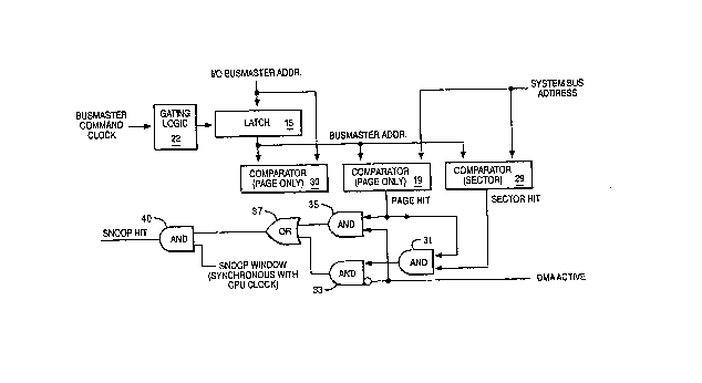
Figure 3 shows the hardware logic u-tilized by the present
invention, and included in IOC~ 7, to determine if a snoop hit
has occurred. Latch 15 receives the address presented by the
I/O busmaster during data transfer operations. The busmaster
device also inputs the command clock of Figure 2
(appropriately conditioned by gating logic 22) to latch 15
which indicates when the memory address is to be latched. In
order to determine if a snoop hit occurs IOCC 7 also includes
a page comparator 19 and sector comparator 29, which receive
an address from system bus 5 correspon~ing to d data location
which is desired by another device connected to the system bus
5 and capable of accessing memory 11. The address in latch 15
is also provided ko comparators 19 and 29 and includes the
memory address of the data in I/O cache 9 being accessed by
I/O busmaster device.
Additionally, a page onl~ comparator 30 is provided which
determines if the busmaster device has requested access to
data on another page, thus causing the system to deactivate
the busmaster and reset the busmaster address latch
synchronously with the CPU clock. The memory address provided
by the busmaster and the memory address from the system bus
are then compared. If the pages are identical, a page hit
occurs and a corresponding signal is output to AND gates 31
and 35. If a the sector addresses are identical, then a sector
hit occurs and a signal is output from comparator 29 to AND
gate 31. If the page hit signal an~ the sector hit signal ar~
both valid, then a signal is output from AND gate 31 to AND
gate 33. Next, a signal indicating the state of the DMA
operation is input to AND gates 33 and 35. The DMA busmaster
active signal is inverted prior to being input to AND gate 33.
The output of both AND gates 33 and 35 are input to an OR gate
37, which then outputs a signal to AND gate 40, which also
212~21~
AT9-93-068 12
receives a signal, defined by the CPU clock (Figure ~)
indicating that snoop comparison is to occur.
Therefore, it can be seen from Figure 3 how the present
invention allows the snoop comparison address granularity to
be dynamic, based upon the state of the DMA busmaster device.
That is, if the DMA siynal of Figure 3 is inactive, then a
valid signal is input to AND gate 33. If both a page and
sector hit occur, based on the signal from AND yate 31, gate
33 will then output a valid signal to OR gate 37. AND gate 40
will then output a signal indicating a snoop hit occurred, if
the signal from OR gate 37 is present when the snoop window
signal is input. Thus, the CPU bus clock is used to determine
the time when the IOCC 7 is to sample its internal logic to
determine if a snoop hit has occurred. In this manner, when
the DMA busmaster device is inactive, snoop comparisons are
implemented on a sector granularity basis. However, if the DMA
active signal is active, then a valid signal will be input to
AND gate 35 and not gate 33. Thus, a page hit signal from
comparator 19 and the DMA active signal will cause a signal to
be output to OR gate 37 and on to AND gate 40. In this manner,
gate 40 will indicate the existence of a snoop hit if the -
snoop hit signal is input while the page hit is present. Thus, - j
as the DMA signal is toggled (changed between the active and
inactive state) it can be seen how the system dynamically
changes snoop comparison granularity between a page address
and a sector address.
:: :
Therefore, the present invention modifies the snoop comparison
logic of IOCC 7 such that the snoop comparison granularity
dynamically changes between a page address portion and the
sector address portion. In this manner the sector address is
completely ignored durinc3 periods of actlvity by a DMA
busmaster device when the device may cause the acldress used
for a snoop comparison to be updated asynchronously.
It can be seen that if page address granularity is used for
snooping operations, it is possible that an active DMA
-` 212~21~
AT9-93 068 13
busmaster device, and ano-ther device on system bus 5 (such as
CPU 1) will want access to data in different memory address
sectors which are on the same page. In this case, a snoop hit
will occur because of the page address granularity. If the DMA
busmaster device is accessing data in cache 9 when a snoop hit
occurs, IOCC 7 then issues an ARTRY signal which tells the
device requesting the da-ta to wait until the DMA busmaster
activity is stopped, at which time IOCC 7 will not intervene
(e.g. cease issuing an ARTRY) to prevent a transfer of
ownership of the data. In this first case, the presen-t
invention avoids non-coherent data between various memory
locations (Ll caches and system memory) in the data processing
system when another device connected to system bus 5 requests
a memory sector address on the same page as a memory sector
address being accessed by a DMA busmaster device.
START
In another case, the active DMA busmaster device may cause a
snoop hit by requesting da-ta which the IOCC must fetch from a
memory sector address which is owned by another device. That
device will detect a snoop hi-t and will hold off the IOCC
while it performs required coherency maintenance actions, such
as writing a modified copy of the requested sector to memory.
When IOCC 7 is unable to provide the data requested by the I/O
busmaster, the IOCC holds off said ~usmaster and de-asserts
(deactivates) its DMA active signal. When DMA is inactive the
IOCC snoops the CPU bus using sector granularity and,
additionally, will respond to a snoop hit by invalidating its
~unmodified) co~y of the requested sector, i.e. the unmodified
copy o the sector in the cache 9 of IOCC 7 is invalidated.
In the previous case, a snoop hit will occur, ragardless of
the memory sector address, since the DMA busmaster device is
active and the snoop comparison granularity is at the page
address level. However, since the DMA busmaster has requested
data with a different page address from the data currently
being accessed (as determined by comparator 30 of Figure 3
when the busmaster device presents an address for a new page),
12~13
AT9-93-068 14
the previously described reset activities occur wherein the
DMA busmaster becomes inactive and the latch 15 of Eigure 3 is
synchronously updated with an address based on the CPU clock.
: . ~
In this manner, I/0 Bus master devices can asynchronously
transfer data between cache 9, and any snoop operation
initiated based on the CPU clock is assured of having a valid
address to use for a snoop comparison since a page address :~
granularity is used. ~-
Therefore, it can be seen that little or no degradation in
system performance will occur by briefly holding off activity
on I/0 bus 13 when a new page is addressed by the busmaster
device.
'::
Those skilled in the art will understand that although the
present invention has been described in terms of a data
transfer between a busmaster device and an IOCC, the present ~: ~
invention will provide cache coherency between any device ~: ;
which accesses data in system memory synchronously with a .
system bus, while its Ll cache is being updated asynchronously :
with respect to the system bus. -~
Although certain preferred embodiments have been shown and
described, it should be understood that many changes and
modifications may be made therein without departing from the
scope of the appended clai.ms.