Note: Descriptions are shown in the official language in which they were submitted.
. .,..YO 93/16512 ? ~ ~ ~ ~ ~ O PC'f/SE93/00023
LASER CONTROL METHOD AND APPARATUS
BACKGROUND OF THE INVENTION
Field of the Inve t~ion
The present invention relates to methods and
apparatus for regulating lasers. More particularly,
the present invention relates to methods and apparatus
for regulating laser diodes.
Des~riution of Re7~at Art
Simulated emission from a GaAs semiconductor diode
laser was first observed in the early 1960's. In the
intervening years, the semiconductor diode laser (the
"laser diode") has come to dominate the laser field in
its technological importance. It has become the key
element in an increasing number of applications, most
notably ~in optical fiber communication and optical data
storage. This "success" is due to the fact that
semiconductor lasers can be simply pumped by passing a
current through them at voltage and current levels that
are compatible with those of integrated circuits, and
because they can be modulated directly at frequencies
in excess of 20GHz. Laser diodes can also be
'~ 93/16512 ~ ~ ~ ~ J ~ ~ PGT/SE93/U0023
-2-
conveniently made because they can be mass-produced by
the same photolithographic techniques as electronic
circuits and because they can be integrated
monolithically with those circuits.
Laser diodes are not without shortcomings,
however. For example, laser diodes typically
demonstrate strong non-linear characteristics for
variations in operating temperature. Thus, the optical
output intensity of a laser diode is difficult to
regulate during variations in operating temperature.
Laser diodes are also known to present considerable
variations: of the light power emitted over tame, that
is, as the laser diodes age.
To moderate the intensity of these variations, it
is necessary to provide. for regulation of the output
light power. Processes are already known for
regulating the light power emitted by a laser diode
under continuous operating conditions in which an
electric signal representative of the light power is
compared with an electric reference signal
corresponding to a reference power. These processes
include means for generating an error signal if
appropriate, and for automatically modifying the
operating conditions of the laser diode upon generation
of such an error signal.
Typically, prior art automatic power controls
supply a bias current that is set at approximately the
threshold current level of the laser diode. In this
manner, When a pulse current is added to the bias
current, the laser diode is effectively switched
between a high and low optical output intensity
corresponding to the wave form of the pulse current.
The supplied bias current is controllably varied to be
approximately at the threshold current level of the
laser diode, particularly when variations in the
VO 93/16512 l PGT/~E93/00023
-3-
threshold current level occur because of corresponding
variations in the operating temperature of the laser
diode.
For clarity and convenience in understanding the
foregoing, a typical digital fiber optical
communication system and the roles of laser diodes and
specific regulators that may be found in such a system
will now be discussed.
A typical digital fiber optical communication
l0 system has a transmitter at a first end and a receiver
at a second end. Between the transmitter and the
receiver are fiber optical contacts, splices, and
optical fiber. The transmitter is an electro-optical
interface which includes an amplifier, laser diode, and
some kind of regulation or circuits for keeping the
laser diode at the same working point. The receiver is
an opto-electrical interface and consists of a
photodiode, generally either of the positive-intrinsic
negative ("PIN") or avalanche photo diode ("APD") type,
an amplifier and clock recovery circuitry.
It is important in digital optical fiber systems
to have as good a power margin as possible. The power
margin is the difference between upper and lower
optical power limits. These upper and lower optical
lower limits are typically set by the receiver. The
upper limit is determined by distortion in the
amplifier caused by overload. The lower limit,
generally called sensitivity, is mainly determined by
noise in the front end amplifier.
3~ The upper limit gives the maximum output from the
' transmitter if there is no damping of the optical
signal in the contacts, splices, and fiber. The lower
limit tells how much power has to be left after the
optical signal from the transmitter has been damped
after passing a number of contacts and splices and
'O 93/16512 ~ ~ ~ ~ 3 ~ ~ PCT/SE93/00023
-4-
kilometers of fibers. The upper and lower limits
define a power budget. Recognizing that every
component in an optical signal path causes some damping
or penalty, it should be appreciated that only a
limited number of contacts or splices or only a limited
length of fiber can be included within any path before
the power budget of that path is depleted. This power
budget may also be decreased by tolerances in both the
transmitter and receiver ends. The tolerance in the
transmitter end is determined by quality of regulation
of the optical output power. All of the aforementioned
relations and penalties are measured in dBm where a
penalty or damping first splice is defined as lOX log
(Pin/Pout)dBm.
As previously mentioned, a laser diode is a
nonlinear element and its characteristics are very
dependent on working temperature and aging effects.
For proper operation, it is necessary to Work over the
knee of the diode. If work takes place under the knee,
the diode will have turn on delay and ringing effects
which may be tolerable but only in small amounts. The
ratio between maximum and minimum optical output power,
the extinction ratio, should be as high as possible but
is limited by maximum mean power and maximum turn on
delay. Regulation has to adjust the working point as
well as possible to compensate for temperature and
aging delays, recognizing that any mismatch between the
ideal and real values will cause a penalty that will
decrease the power budget.
One of the most common ways to regulate a laser is
to have the laser diode work at a constant temperature
by a regulated peltier element. Such regulators
contain two regulation loops, one for the peltier
element and one for the mean power regulation. The
output power regulator senses the mean optical output
~' JVO 93/16512 '~ ~ ~ ~ ~ ~ a PCT/SE93/00023
-5-
power with the monitor pin diode, and adjusts the bias
current to compensate for the by-age increased Ith or
threshold current. In such cases changes in scope
efficiency are quite small. This kind of regulation
works well but is expensive to implement, has a high
power consumption (that is, a couple of watts for
temperature regulation), requires cooling, and consumes
space. Further, the peltier element is not as reliable
as the laser diode.
As previously mentioned there are a number of
alternative methods to regulate a laser without
temperature regulation. One such method is to have
only mean power regulation. Such a method has a
constant modulation current and a simple,regulation of
the bias current. This method gives a penalty of 5-6
dBm's for a PIN receiver and more for a APD receiver.
Another method, slightly more complex, is to
complement a mean power regulator with a simple feed
forward regulator for the modulation current. By
sensing the temperature and predicting the modulation
currents of the laser diode compensation for variations
of slope efficiency can be made. This method is very
simple but it requires matching between the sensing
element and the characteristics of the laser and does
not compensate for aging. This method gives a penalty
of a couple of dBm's.
A third method is to regulate mean power as above
and also to regulate the madulation power via some kind
of low frequency modulated optical power. The optical
output power is modulated with a low frequency signal,
the amplitude of the signal being ~10% or less of the
data signal's amplitude so that it can be seen as an
low frequency ("hF") ripple on the signal. Modulatian
can be done via the bias current and causes both
maximum and minimum optical values to vary. If such
~O 93/16512 ~ ~ ~ ~ j ~ ~ PCT/SE93/00023
-6-
modulation is done completely above the knee these
variations would be the same for bath maximum and
minimum power, but if the bias current is decreased
close to the knee or slightly under it, the minimum
output power variations will be suppressed. This
variation of the LF signal will be registered by the
monitor and filtered away and used for regulation
together with the mean power signal. This third method
has a penalty of approximately a dBm caused by the LF
modulation. Additionally, regulation of this method
can only work close to the knee for proper regulation.
The optimal working point can at some times be out of
this range.
SUr9~IARY OF THE INVENTION
The present invention overcomes the shortcomings
and deficiencies of the prior art by providing an
apparatus for controlling the optical output intensity
of a laser diode. The apparatus according to the
teachings of the present invention includes first means
2o for receiving a portion of the optical output of the
laser diode and delivering a first signal having a
magnitude representative of the mean output intensity
of the laser diode optical output, second means for
receiving a portion of the optical output of the laser
diode and delivering a second signal having a magnitude
representative of the peak output intensity of the
laser diode optical output, third means for comparing
the magnitude of the first signal to a reference
current signal and adjusting the mean output intensity
so that it remains substantially constant: and fourth
means for comparing the magnitude of the second signal
to a reference current signal and adjusting the peak
output intensity so that it remains substantially
constant.
CA 02125390 2003-O1-21
Embodiments of the present invention may also
include structure operable to perform data clocking, such
as a D-latch.
The first means and third means effectively form a
mean power regulation loop, the second and fourth means
effectively form a peak power regulation loop. In
embodiments of the present invention, the mean power
regulation loop and the peak power regulation loop may
operate with a same predetermined time constant.
In apparatus according to the teachings of the
present invention the third means may comprise a
modulation regulator and/or the fourth means may comprise
a biasing regulator. Additionally, apparatus according
to the teachings of the present invention may include a
laser and/or data failure alarm. Still further, apparatus
according to the teachings of the present invention may
include a narrowband channel and a broadband channel.
According to the teachings of the present invention,
a method for controlling the optical output intensity of a
laser diode used in an optical communication system to
periodically transmit data, in which the laser diode
receives current from a pulse current supply and a bias
current supply, includes the steps of (a) receiving a
portion of the optical output of the laser diode and
delivering a first signal having a magnitude
representative of the mean output intensity of the laser
diode optical output; (b) receiving a portion of the
optical output of the laser diode and delivering a second
signal having a magnitude representative of the peak
output intensity of the laser diode optical output; (c)
comparing the magnitude of the first signal to a reference
current signal and adjusting the mean output intensity so
that it remains substantially constant; and (d) comparing
CA 02125390 2003-O1-21
8
the magnitude of the second signal to a reference current
signal and adjusting the peak output intensity so that it
remains substantially constant.
Steps (a) and (c) effectively provide a mean-power
regulation loop, and steps (b) and (d) effectively provide a
peak-power regulation loop. In embodiments of the present
invention, the mean-power regulation loop and the peak-power
regulation loop may operate with a same predetermined time
constant, provided by a data-clocking step.
Accordingly, in one aspect the present invention
provides a laser driver which is not sensitive to DC
imbalance of transmitted data signal.
Another aspect of the present invention is the
provision of a laser driver using a relatively small time
constant in its regulation loops.
A feature of the present invention is its provision
a laser driver in which process, temperature and supply
variations are suppressed.
By another feature the present invention is able to
provide a laser driver in which a working point, both
under and over biased, can be readily chosen.
Other advantages and novel features of the present
invention will become apparent from the following
detailed description of the invention when considered in
conjunction with the accompanying drawings wherein:
FIG. 1 depicts a typical Ga.As~Gal_"AlXAs laser;
FIG. 2 depicts the conduction and valence band edges
under large positive bias in the laser of FIG. l;
FIG. 3 depicts the index of refraction profile and
optical field (fundamental mode) profile relating to FIG. 2;
FIG. 4 a,s a graph illustrating typical laser diode
behavior based upon temperature changes and aging;
FIG. 5 is a graph illustrating various variables
involved in modulating a laser diode; and
FIG. 6 is a block diagram of a laser driver
according to the teachings of the present invention.
~'O 93/16512 ~ ~. ~ 5 3 J 0 PCT/SE93/00023
_g_
Referring now to the drawings wherein like or
similar elements are designated with identical
reference numerals throughout the several views, and
more particularly to FIG. 1, there is shown a laser
diode 10. Laser diode 10 will be discussed in some
detail below to facilitate understanding of the laser
diode control method and apparatus of the present
invention. .
As is known to those skilled in the art, the high
l0 carrier densities needed to obtain gain in
semiconductors can be achieved with moderate current
densities~~near the junction region of a p-n diode. The
most important class of semiconductor diode lasers are
based on III-V semiconductors. One system is based on
GaAs and Ga~_xAlxAs. The active region in this case is
GaAs or Ga~_xAlxAs. The subscript x indicates the
fraction of the Ga atoms in GaAs that are replaced by
A1. The resulting lasers emit (depending on the active
region molar fraction x and its doping) with a
wavelength between about .0'75 and 0.88 microns. This
spectral region is convenient for short-haul (<2km)
optical communication in silica fibers.
A second system has Ga~_xIn~rs~_yPy as its active
region. The lasers emit in the 1.1 to 1.6 micron
frequency spectral region depending on x and y. The
region near 1.55 microns is especially favorable, since
optical fibers with losses as small as 0.15 d8/lan at
this wavelength are available, making it extremely
desirable for long-distance high data rate optical
communication.
Referring now specifically to FIG. 1, there is
shown a generic GaAs/Gay_xAlXAs laser diode l0. This
laser diode 10 has a thin (0.1 - 0.2 micron) region of
GaAs 12 that is sandwiched between two regions of Ga~_x
Alx As of opposite doping 14, 16, thus forming a double
VO 93/16512 ~ 3 ~ Q PCT/SE93/00023
-10-
heterojunction. The contents of FIG. 2 helps explain
the reasons for this structure. FIG. 2, as mentioned
in the brief description of the drawings section above,
shows the conduction and valence band edges (designated
by reference numerals 18 and 20, respectively) in a
typical heterojunction diode at full forward bias: A
key element in this structure is the formation of a
potential well for electrons of height delta E~ 22 that
coincides spatially with a well for holes of height
delta EN 24. The energy gap discontinuity is due to its
dependence in Gay_x Alx As on the A1 molar fraction x.
Under forward bias with eVa ' Eg, the large densities
of injected electrons (from the n side) and holes (from
the p side) in the well cause the inversion condition
in that region to be satisfied so that radiation at
omega satisfying the equation
EFe - EF~ > h bar (that is, Planck's constant
divided by 2 pi) times omega.
2A is amplified in the well. This GaAs inner layer where
stimulated emission 'takes place is called the active
region. For maximum gain, it is necessary to confine
the light as tightly as possible to the active region
since light travelling outside this region does not
give rise to stimulated emission, thus not contributing
to the gain. This confinement is brought about by a
dielectric waveguiding effect due to the fact that a
lowering of the energy gap of a semiconductor causes an
increase in the index of refraction so that the Ga~_x
Alx As/GaAs/Ga~.x Alx As sandwich acts as a dielectric
waveguide with the modal energy concentrated in the
active region. The index distribution and the modal
yfO 93/16512 I j ,/, ~ c'~ ~ V j'(: «S~ysiuvucs
-11-
profile of a typical heterojunction laser is shown in
FIG. 3. The index of refraction dependence on x is
delta n, which is approximately equal to - 0.7x.
Referring now to FIG. 4, there is graphically
shown typical laser diode behavior, which behavior was
discussed in the description of related art section
above. FIG. 4 shows that laser diode threshold current
increases and slope efficiency (dP/dI) decreases as
ambient temperature increases and/or the laser diode
ages.
FIG. 5, as previously mentioned, shows a number of
significant variables involved in modulation of a laser
diode. In FIG. 5, Ib;as denotes the bias current and I~
the modulation current. P~ is the maximum optical
power or peak power. The extinction ratio, also
discussed in the description of related art section
above, is P~ P";n.
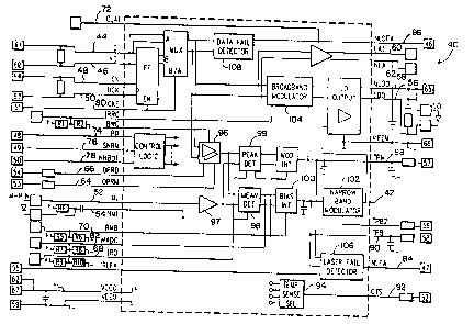
Referring now to FIG. 6, there is shown a laser
driver 40 according to the teachings of the present
invention. This driver 40 comprises simple hardware
relative to prior art drivers and, further, allows
integration of a relatively large number of functions
on a single chip. Recognizing that dashed line 42 may
be considered to designate the boundary of an
integrated circuit ("IC"), an IC according to the
teachings o~ the present invention contains, as will be
discussed in detail below, high current output stages,
control loops, and maintenance perfor~aing structure.
The driver also features a broadband and a narrowband
channel.
"~'O 93/16512 ~ ~ ~ ~ pCT/SE93/OIy023
-12-
With regard to the data/HF interface of the driver
40, data input signals Dl/NDl (true/not true,
respectively) are shown and represented in FIG. 6 by
reference numerals 44 and 46. Likewise, clock input
S signals CIC/NC1C (true/not true, respectively) are shown
and represented in FIG. 6 by reference numerals 48 and
50 and monitor input MI/NMI (with max input current
being 1 mA) are shown and represented in FIG. 6 by
reference numerals 52 and 54. Data/HF interface output
comprises laser diode output signal LDO, laser diode
output inverted signal NLDO, and maintenance loop A1
true and inverted outputs LA1 and NLA1. The foregoing
output signals are shown and represented in FIG. 6 by
reference numerals 56, 58, 60 and 62, respectively.
With respect to control and Y-interface signals,
there are two basic analog input signals to driver 40.
They are the optical power reference for modulation
signal oPRM~and the optical power for biasing signal
OPRB. The OPRM signal provides a reference input for
adjusting the modulation value of the optical output
power, that is, the level difference between optical
'1' and optical '0'. The OPRB signal, on the other
hand, provides a reference input for adjusting the mean
value of the optical output power. The OPRM signal and
the OPRB signal are shown and represented in FIG. 6 by
reference numbers 64 and 66, respectively.
There are a number of extra inputs to the driver
circuit 40. Generally, these inputs are for testing
purposes. Via these inputs, the values of internal
references may be changed. All of the internal
references within the driver circuit 40 have their own
default values: however, these defaults can be changed
if desired by adding an external reference current.
Every internal reference source with an external
reference input works in the same way. If an external
JVO 93/16512 ~ ~ ~ ~ ~ ~ ~ PCT/S~93/00023
-13-
reference input is low (e.g., lower than -4V), the
default value is used. If a current is applied to the
input it will go high (e. g., over -4V). This will
effectively turn off the internal reference source and
effect a mirroring of the external current for use as
new internal reference.
Four of the aforementioned extra inputs are SRC1,
SCR2, IRD, and IRMB. SRC1 and SRC2 may be connected to
the Y-interface and may be adjusted externally outside
the TR-module if necessary. SRC1 and SRC2 are
effectively for slew rate control. SRC1 and SRC2
provide reference input for controlling the positive
and negative slope of the laser output signal to
optimize the signal for each implementation if the
default values are not sufficient. It is not necessary
to connect the SRC1 and SRC2 signals directly to the Y°
interface and those signals can be adjusted directly on
the TR module. The default value for SRC1 can be about
100 uA. The default value of SRC2 can be about 0.4% of
the modulator current.
It is important to note that the SRCl and SRC2
signals discussed in the immediately preceding
paragraph merely constitute certain aspects of certain
embodiments of the present invention. Other
embodiments of the present invention, which embodiments
lack SRCl and/or SRC2 signals and/or those signals as
described hereinabove, are possible. For example, in
an embodiment of the present invention which has been
actually constructed, the signals SRC1 and SRC2
described above have been replaced with a single signal
designated IRRC, which signal performs the SRCl and
SRC2 functions described above. Such modifications
should be appreciated and understood to be aspects of
the present invention within the scope of the appended
claims.
/O 93/16512 ~ ~ ~ PGT/SE93/00023
-14-
The IRD and IRMB signals can only be adjusted
internally on the submodule. The IRD signal provides
a reference input for the current and the detector
circuit. Default value for an IRD signal can be about
10 uA. The IRMB signal provides a reference input for
the current in the integrator circuits, mod reg and
bias reg. A typical default value for an IRMB signal
may be about ZO uA.
FCl and FC2 are frequency compensation
connections. These connections are for compensation of
the slow monitor PIN diode. The peak value of the
monitor signal will be dependent upon the frequency
spectrum in the data signal. This causes a dependence
in the optical output level when alternating between
different frequency spectres around or over the
bandwidth of the monitor PIN diode. This dependence
can partially be compensated for by connecting an
inductor between FC1 and FC2. An example value of this
inductor could be about 50 nH. This compensation can
also be omitted during the manufacturing process or by
simply connecting a jumper between the two pads.
An alternative solution has been implemented by
the inventor of the present invention for this
bandwidth compensation. An extra input, BWC (bandwidth
control), may be added to the circuit. This input can
control the bandwidth of the data reference signal
through the amplifier 96 so that the output signal from
the circuit 96 will almost look the same as the output
signal from the monitor amplifier 97. This function
can increase the usable bandwidth region for the
circuit which leads to a proper regulation even if
there is a bandwidth limitation in the monitor diode.
With respect to digital input, there are a number
of signals appropriately mentioned. In this
discussion, CMOS levels referred to are negative 5
r ,WO 93/16512 ~ ~ ~ ~ 3 9 ~ PCT/SE93100023
-15-
volts so that high or H is equal to 0 volts and low or
L is equal to negative 5 volts. The closed loop A1 or
CL~rl signal 72 closes the loop A1 by enabling the loop
A1 output. H is equal to loop A1 connected. Power
down or PD signal 74 is a power down command input.
For this PD signal high is equal to power down. ~ The
select narrow band mode or SNBM signal 76 sets the
laser driver 40 in a narrow band traffic mode. For
this signal high is equal to enabled. The narrow band
data input or NNBDI signal 78 is a negative narrow band
data input when the laser driver works in the narrow
band traffic mode. CMOS levels refer to negative 5
volts, inverted. High on the input gives no optical
output power. For the aforementioned PD, SNBM and
NNBDI signals in a driver 40 according to the teachings
of the present invention, the following truth table may
be employed:
~'HUTH TABLE
PD SNBM NNBDI
H L X Power down
mode
H H X Narrow band
operating
mode
L X X Broad band
operating
mode
The clock enable or CKE signal 8o enables clocking of
the data signal. For the CIA signal high is equal to
clocked data. An NADC signal 82 adds extra capacitance
to the peak detector in the detector circuit if
necessary. Low gives extra capacitance. This is
connected by a jumper on the subcarrier.
Two digital output signals are a negative laser fail
alarm or NLFA signal 84 and a negative laser data fail
alarm NLDFA signal 86. The NLFA signal 84 alarms if
WO 93/16512 ~ ~ 2 ~ 3 9 0 PCT/SE93/00023
-16-
there is no optical power detected in the monitor. For
this signal, low is equal to alarm. The NLDFA signal
86 alarms when there is no current data on the data
input. For this signal, law means alarm.
Driver 40 has five test points situated close to the
driver chip for testing of internal signals in
connecting external compensation components. These
five test points are designated TPM, TPB, CTS, TPl and
TP2. The TPM test point 88 is for test point
ZO modulation. The TPB test point 90 is for test point
bias. TPM and TPB are for regulating voltages. It is
possible'.to override this inherent regulation by
forcing these test points, which allows external
regulation of the optical signal. External capacitors
can also be connected to these test points if it is
necessary to increase the time constants in the
integrators. The CTS test point 92 relates to chip
temperature. A temperature sensing component 94 is
associated with this test point 92. In embodiments of
the laser driver 40 of the present invention, a number
of temperature sensors can be placed at different
places on the chip. These sensors can be selected one
at a time and connected to the output CTS. These
sensors may be selected by the signals NNBDI and SNBM.
TP1 and TP2 are optional test points.
~lith respect to function, the laser diode driver 40
consists of six parts: a data clocking and signal
path, a modulation regulator, a biasing regulator, a
modulator, a supervisory part, and a part for low power
bit rate reduced traffic, that is, narrow band traffic
at about 200 kilobits per second. In, general, in
embodiments of the present invention narrowband
modulation works to a range from 0 up to some number of
M/bits/s and broadband modulation works from P~its/s up
1VQ 93/16512 ~ ~ ~ ~ 3 ~ fl PCT/SE93/00023
-17-
to Gbits/s. Each of these parts will be described in
individual paragraphs immediately below.
The data clocking and signal path comprises a D-latch
for clacking of the input data. This path further
comprises a driver for an extra output, that is, loop
A1 output. The extra output is enabled by a control
signal. In general, this path handles internal
distribution of data. In embodiments of the present
invention, the D-latch itself can be bypassed by a
control signal.
The modulation regulator comprises the modulation
current regulator. In this part the opticar '1' level
is detected by a monitor diode and compared with the
"OPRM" reference signal. This comparison is done in
element 99 and it effectively detenaines the optical
amplitude, optical '1' - optical '0', on the laser
diode°s P/I transfer curve. In embodiments of the
present in~rention, the modulation is always adjusted so
that the optical amplitude power level remains
constant. The functions performed by this part
effectively compensate for variations in the external
differential efficiency of the laser diode due to
temperature and aging effects.
The biasing regulator part of the laser driver 40
comprises a biasing current regulator. In this part
the optical mean level is detected by the monitor diode
and compared with the "OPRB" reference signal. By
means of this regulator, specifically elements 98 and
100 shown in FIG. 6, the bias current from the laser
driver circuit is regulated together with the
modulation current so that the optical ' 0' output power
is always constant. The functions performed by this
part effectively compensate far variations of the
threshold current due to aging and temperature
variations. This part and the modulation part 102
'O 93/16512 ~ ~ ? ~ j 9 4 PCT/SE93/00023
-18-
together hold the optical output power levels for the
'0' and '1' constant and independent of ambient
temperature, supply voltage variations, aging effects
of the laser diode, and the like.
The comparison effected within this portion of a
laser driver according to the teachings of the present
invention constitutes a significant advance aver the
prior art and a matter of particular interest to those
skilled in the relevant art. In general, a comparison
is made between the "data voltage reference" and the
"monitor voltage reference". More specifically, a
comparison between the peak values and mean values,
respectively, is made for those two voltages.
Continuing the discussion immediately above, it
should be appreciated that the method by which the two
voltages are created causes them to be electrically
equal. Thus, modulator 96 and monitor front end 97
(see FIG. 6) provide a symmetric balance. Summarizing
the foregoing, it may be said that the two reference
currents control a modulator 96 that modulates the data
signal to an internal reference voltage. The monitor
current converts in a monitor front end 97 to a monitor
voltage. Accordingly, the two reference currents
mirror the mean and peak current in the monitor current
and the data signal mirrors the data pattern in the
monitor signal.
The modulator comprises the output laser driver
stages and an adjustable modulation controlling
circuit. Elements 102 and 104 shown in FIG. 6 form
part of this modulation. The adjustable modulation
controlling circuit controls the positive and negative
slope of the laser diode output. Rise and fall time of
the signal can be adjusted to optimize the signal for
the laser diode and for the connections between the
driver and a laser associated therewith. This facility
7V0 93/16512 ~ ~ ~~ ~ (~ ~ PCT/SE93/00023
-19-
allows partial reduction of the penalty caused by
mismatch in laser diode connections, which connections
differ in different implementations.
The supervisory part of the laser driver perfonas two
supervisory functions. One such function is a laser
failure alarm. This alarm 106 activates in the event
of a failure in a laser or a monitor. The alarm
circuit senses the two regulation voltages TPB and TPM
and if one or both are stuck to the limiting power
supply rails for the circuit that will indicate that
the regulation is out of order and, in turn, that the
laser is out of order. At that point, the output alarm
may and should be triggered. The second function is a
data failure alarm. This alarm 108 activates when
there is no current data to transmit on the data input .
The low power/narrow band traffic portion of the
laser driver 40 handles low power bit rate reduced
traffic. The narrow band has a bit rate of from 0 to
some Mbits/s. The ISDN U-interface for 2B+D has a bit
rate of 160 kilobits per second. Power is saved by
using a low bandwidth and a modified modulation method
of the laser. Typically, a laser Works by being
completely on or completely off. When optical 1's are
transmitted the laser works as usual with the same
power level as determined by the "OPRB" and "OPRM'°
references. When optical 0's are transmitted the bias
is turned off. In such a case, the incoming narrow
band data stream modulates the laser directly. Power
dissipation is also decreased by using bi-phase coding
and by shortening the pulses. The narrow band part
uses the bias current stage to modulate the laser
rather than the modulator 104.
From the foregoing description and the accompanying
drawings, it may gathered that the laser driver of the
present invention relies upon a bipolar-CMOS process.
'"WO 93/16512 ~ ~ ~ ~ ~ (~ O PCT/SE93/00023
-20-
The process of the present invention is generally
intended for digital applications. More specifically,
a laser driver chip serves as an interface between an
electrical path and a laser diode. The Laser driver
chip according to the teachings of the present
invention may be used in other, similar applications.
By way of example only, set forth below are
recommended operating conditions, electrical
characteristics, and control signal/Y-interface signals
for one embodiment of the present invention.
Recommended Operating Conditions
Power supply min 4.5 V nom 5.0 vmax 5.3
V
Current max 200mA
operating temperature 0 - 7o C
~Iectrical Characteristics
Data/HF Interface
All values are referred to 0 and -5 V supply voltage.
Data/Clock input
min input level peak to peak 300 mV
common mode range -3 - -0.3 V
max input current (sinking) 10 uA
capacitive load max 2 pF
Data output (LA1)
Terminating load 150 ohm, max capacitive
load 5 pF
min output level peak to peak 200 mV
output range min - max -1.4- -0.9V
max rise and fall time (l0-90%) 0.8nS
Monitor input
max current from NMI to MI l.mA
voltage level of MI -4.2 - -4.0 V
voltage level of NMI 0.0 V
. 1 ~1~V0 93/16512 ~ ~ ? '~ ~ ~ ~ PCT/SE93100023
-21-
Laser diode output, LDO
max modulation current, Im 50 mA
max bias current, Ib 100 mA
max modulation current in narrowband operation
Imn 100 mA
Laser diode output negative, NLDO
max modulation current 50 mA
Control Sianals/Y-Interface Sicrnals
Analog input
OPRM modulation reference current input
reference, current 0.1 - 1 mA
voltage level -4.2 - OV
OPRB bias reference current input
reference current 0.1 - 1 mA
voltage level -4.2 - OV
SRC1/SRC2, external reference input for controlling
slopes in output signal to the LD is necessary.
Disabled, voltage level lower than -4 V
Those skilled in the art should now appreciate that
the laser driver according to the teachings of the
present invention effects comparison between real
values from a monitor diode and desired values from an
internal network. These two.data paths are virtually
identical. The mean current and peak current for the
monitor is mirrored by the two external reference
currents OPRB and OPRM. The data signals from the
monitor amplifier and the data amplifier look the same.
Ali of the foregoing give rise to a number of
advantages. One such advantage is suppression of
~~'O 93/16512
PC'TISF.93/00023
-22-
pattern variations. The circuit according to the
teachings of the present invention is not sensitive to
DC imbalance of the transmitted data signal:
Furthermore, the comparison between two almost
identical signals allows for reduction in the time
constant in the loops. Still further, the two
regulator loops, the peak power and the mean power,
modulator and bias, cooperate. Their time constants
can be the;same. This is opposed to other systems in
which a difference of 5 to 10 times is necessary.
Still further, an almost perfect symmetry~in operation
suppresses process, temperature and supply variations.
The laser driver of the present invention effects very
accurate regulation. Mean and peak regulation allows
choosing desired working point under and over bias.
~bviously, numerous modifications and variations are
possible in light of the above teachings. For example,
while the specific embodiment of the present invention
described herein is made for a digital data stream, an
embodiment of the present invention could also be made
for an analog application where the data stream is a
sinusoidal signal which is frequency modulated, phased
modulated, or modulated in some other way. As another
example, the inventor of the present invention. has
chosen a mean and peak combination (Note: there are
three different detectors for measuring two points on
'JO 93/16512 ~ ~ 2 ~ 3 ~ p PGT/SE93/00023
-23-
the P/I curve for the laser diode, valley-, mean- or
peak-detector, and there are three possibilities for
combining these detectors; valley and mean, valley and
peak, or mean and peak) herein because mean detection
is simple and accurate and if peak detection does not
work there should be at least a working mean power
regulation. Those skilled in the art should
appreciate, however, that the mean detector may be
replaced with a minimum peak or valley detector in
1~ laser control apparatus. In fact, such a valley and
peak combination would probably give a very accurate
regulation if the P/I curve for the laser diode is bent
and the radius of the bend is temperature dependent
(which happens with some laser diodes, especially when
there is a high driving current and high temperature).
From the circuit s point of view, there is a very
simple way to effect these changes. That is, to
substitute the detectors to the preferred combination,
with the first detector as block 98 and the second as
block 99. When such detector blocks are used, of
course, valley value instead of mean value will be
detected. Functionally, however, everything, including
the rest of the circuit, will remain the same. Other
changes and variations leading to other embodiments of
the present invention are possible. Accordingly,
within the scope of the appended claims, the present
'-'y0 93/16512 ~ ~ PGT/SE93/00023
-24-
invention may be practised otherwise than as
specifically described herein.