Note: Descriptions are shown in the official language in which they were submitted.
--' 2~2~827
LEVEL CONVERSION CIRCUIT
The present invention relates to a level conversion
circuit for converting a digital input signal varying between
first and second voltage levels to a digital output signal
varying between said first level and a third voltage level,
and including b~tween first and second poles of a DC supply
source the series connection of the main paths of a first
transistor and of a second transistor, to the control
electrode of which said input signal is applied.
Such a level conversion circuit is already known in
the art, e.g. from the published European patent application
EP 0 3~8 074 A1. Therein, the first and second transistors -
are of opposite conductivity type and two further third and
fourth transistors are coupled between the two DC supply
poles in a si~ilar way as the first and second transistors
and in parallel to the series connection of the latter
transistors. The first and third transistors are of PMOS
conductivity type, and the second and fourth transistors are
of NMOS conductivity type. The complement of the input signal
is applied to the gate electrode of the third transistor. The ~ -~
~unction point between the third and fourth transistors
constitutes a true output terminal of the level conversion
circuit, and the junction point between the flrst and the
second transistor constitutes a complemented output terminal.
The gate electrode of the second transistor is connected to
the true output terminal, whereas the gate electrode of the
fourth transistor is connected to the complemented output
terminal. The voltage provided at the first DC supply pole is
0 volts and the voltage provided at the second DC supply pole
is 5 volts. ~ --
Such a level conversion circuit is for instance
used to convert a digital input signal varying between 0
volts and 3.3 volts to a digital output signal varying
between 0 volts and 5 volts, the digital input signal being
provided by circuitry operating with a 3.3 volt supply
':
D. SALLAERTS -- L. Cl,OETEl~S 10 -- 7
'-.'
::
:.
~ 212~827
voltage as is necessary when the conductor line widths are so
small and the gate oxide layers are so thin that the use of
e.g. a 5 volts supply voltage would cause prob]ems of metal
electromigration and hot electron effects, respectively. The
latter digital signal is then applied to circuitry operating
with a 5 volt supply voltage. To be noted that the problem of
metal electromigration is due to the current through the
conductor, i.e. smaller conductor line widths necessitate
lower currents and thus lower supply voltages.
When the input signal is high, i.e. 3.3 volts, the
first transistor is turned on and the third transistor is
turned off. As a result, the voltage at the complemented
output is low and the fourth transistor is turned on, thereby
causing the voltage at the true output terminal to be high
and the second transistor to be turned off. Across the main
paths as well as across the gate drain junctions of both the
second transistor and the third transistor a voltage drop of
5 volt is produced. Across the gate drain junction of the
fourth transistor also a voltage drop of 5 volt is produced.
For an input signal which is low similar conclusions apply.
Thus, it is clear that together with tt-e input
signal a complemented version thereof is needed in the above
level conversion circuit. Furthermore, when the level
conversion circuit is integrated on a chip operatiny with a
3.3 volt power supply necessary because of small line widths
and thin gate oxide layers thereon, then problems due to
metal electromigration and hot electron effects may occur
since voltage drops across the transistors may rise up to 5
volts instead of the maximum allowed 3.3 volts, which is the
,maximum of the input voltage.
An object of the present invention is to provide a
level conversion circuit of the above known type but wherein
no complement of the input signal is needed and wherein
voltage drops across the transistors of the circuit are in
absolute value limited to the maximum of the input voltage.
D. SALLAERTS - L. CLOETENS 10 -- 7
---" 212~827-
- 3 -
According to the invention, this object is achieved
due to the fact that said level conversion circuit further
includes a load impedance between said first DC supply pole
and an output terminal connected to said series connection,
wherein said second transistor, which is of a same first
conductivity type as said first transistor, is connected in
parallel to a main path of a third transistor of a second
conductivity type opposite to said first conductivity type,
and whose control electrode and that of said first transistor
are biased by a constant DC bias voltage, the junction point
of said load impedance and said series connection
constituting an output terminal of the conversion circuit.
In this way, because of the DC bias voltage applied
to the control electrode of the first transistor, this -~
transistor isolates the second transistor from the second DC
supply pole so that the voltage across any two poles of this
first transistor is prevented from rising above the maximum
input voltage. Indeed, when the input signal is equal to the
first voltage level, then the second transistor is turned off
and the voltage across its main path rises until a limit
voltage which causes the fi.rst transistor to be also turned
of~. The latter limit voltage depends upon the DC bias
voltage applied to the control electrode of the second
transistor. Furthermore, in order to avoid that due to a slow
charging of parasitic capacitances present at the junction
point between the first and the second transistor the voltage
thereat would rise too much above the mentioned limit
voltage, the third transistor is provided which when the
voltage at the latter junction point becomes too high is
turned on thereby reducing the latter voltage until the third
transistor is turned off again. Thus, the voltage at the
junction point between the first and the second transistor is
limited to a voltage between a minimum value below which the
second transistor is turned on and a maximum value above
which the third transistor is turned on. The latter values
can be so chosen that the voltage across any junction of the
D. SALLAERTS - L. CLOETENS 10 - 7
~,
` ~ 212~27
- 4 -
first, second or third transistor is at most equal to the
maximum input signal level. Furthermore, it is clear that no
complement of the input siqnal is needed.
Another characteristic feature of the present
invention is that said level conversion circuit includes a
level clamping circuit.
In this way, a protection against too high and too
low a voltage on the output terminal is provided.
The above mentioned and other objects and features
of the invention will become more apparent and the invention
itself will be best understood by referring to the following
description of an embodiment taken in conjunction with the -
accompanying drawing which shows a level conversion circuit
according to the invention. --
This level conversion circuit is used to convert a
first digital signal varying between 0 volt and 3.3 volt
applied to an input terminal IN to a second digital signal
varying between 0 volt and 5 volt provided at an input/output
or output terminal OUT, and to convert a third digital signal
varying between 0 volt and 5 volt applied to the input/output
terminal OUT to a fourth digital signal varying between 0
volt and 3.3 volt provided at an output terminal OUT2. The
first and fourth digital signals are for instance used in
circuitry operating with a 3.3 volt supply voltage, whereas
the second and third digital signals are used in circuitry
operating with a 5 volt supply voltage. Such level conversion
circuits become necessary when small line widths and very
thin gate oxides raise problems of metal electromigration and
hot electron effects, thereby ruling out the possibility of
a 5 volt supply voltage and necessitating the use of a lower
supply voltage, e.g. 3.3 volt, when, moreover, such 3.3 volt
circuits are to be used together with circuits operating with
a 5 volt supply voltage, and when one wants to implement the
circuit on a 3.3 volt integrated circuit, i.e. whPre no gate
or junction voltage may rise above 3.3 volt in order to avoid
the above mentioned problems. It is evident that other supply
D. SALLAERTS - L. CLO~TE~S 10_- 7
--~ 2~2~827
voltage combinations than the above 3.3 volt/5 volt are
possible.
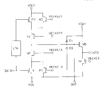
The level conversion circuit shown in the drawing
includes between a positive pole VDD2 of a DC supply source
providing a like named positive supply voltage and a negative
pole VSS thereof providing a like named negative supply
voltage the series connection of source drain paths of a PMOS
transistor P2 and of a PMOS transistor P3 and drain source
paths of an NMOS transistor N1 and of an NMOS transistor N2.
The source drain path of a PMOS transistor P1 is coupled in
parallel to the drain source path of N1, and the drain source
path of an NMOS transistor N3 is coupled in parallel to the
source drain path of P2. The gate of N2 is biased by a DC
bias voltage VBIAS1A and that of P1 by a DC bias voltage
vsIAs1s, whereas the gate of N3 is biased by a DC bias
voltage VBIAS2A and that of P3 by a DC bias voltage VBIAS2B.
The input terminal IN is coupled to the gate of N1 and via a
level shift circuit LSH to the gate of P2. Such a level shift
circuit merely duplicates the digital signal applied to IN at
a higher level and is e.g. described i.n the book 'Analog MOS
integrated circuits for signal processing' by R. Gregorian
e.a., J. Wiley & Sons, 1986, pp. 200 to 203. In order to be
able to turn off transistor P2 completely, the output signal
~ ~S~ mus h~Ye ~ high ~eve~ equa~ to VDV2. ~he
2S interconnected drains of N2 ~d P3 consti~ute the
input/output terminal OUT which is connected to a clamping
clrcuit which ls constituted by a diode or diode means D2
whose anode is connected to VSS and whose cathode is
connected to OUT, and a diode or diode means D1 whose cathode
30 is connected to a positive pole VDD1 of the DC supply source
providing a like named positive supply voltage and whose
anode is connected to OUT. The level conversion circuit
further includes between VDD1 and VSS the series connection
of drain source paths of two NMOS transistors N5 and N4. The
gate of N5 is connected to the input/output terminal OUT, and
the gate of N4 is connected to a DC bias voltage VBIAS3. The
D. SALLAERTS - L. CLOETENS 10 - 7
-` 2125827
- 6 -
connecting terminal between N4 and N5 constitutes the output
terminal OUT2.
To be noted that the part P2, P3, N3 of the circuit
can be seen as a load impedance for the part N1, N2, Pl of
the circuit, and that it may also be replaced by a load
impedance proper. Such a configuration is referred to in
literature as an open drain configuration. In that case, LSH
is no longer needed. Furthermore, when the input signal is
high a DC current will then flow from positive supply pole
VDD2 via transistors N2 and Nl to VSS thus giving additional
power dissipation, whereas no such DC current flows in the
circuit shown in the drawing, as will become clear
hereinafter.
The values of the supply and bias voltages are
given in the following table.
. _ , _
VSS 0 volt
VDDl 3.3 volt
VDD2 5 volt
VBIAS1A 3 volt
20 VBIAS1 B 2 volt
VBIAS2A 3 volt
VBIAS2B 2 volt
¦ VBIAS3 see text
_ _ -
Also, since the input signal of the level shift
circuit LSH varies between 0 volt and 3.3 volt and since its
output must be a digital signal with a high level of 5 volt
(VDD2), the latter output digital signal varies between 1.7
volt correspond:ing to a 0 volt input level and 5 volt
corresponding to a 3.3 volt input level.
The operation of the level conversion circuit is
now described hereinafter. First the conversion of a digital
signal varying between 0 and 3.3 volt to one varying between
0 and 5 volt as performed by the upper part of the circuit is
considered.
D. SALLAERTS - L. CLOETENS 10 - 7
-~ 212S827
- 7 -
When the voltage at IN iS high, i.e. 3.3 volt, then
N1 is turned on and the voltage at its drain is pulled down. -~
When the latter voltage is at the so-called threshold voltage
VTN2 Of N2 below VBIAS1 A then N2 iS turned on. At the same
time a 5 volt signal is applied to the gate of P2 via LSH, so
that P2 iS turned off and the voltage at its drain drops
until it is at the absolute value of the threshold voltage
¦VTP3¦ of P3 above VBIAS2B at which point P3 1S also turned
off. Here, ¦.¦ denotes the absolute value. N3 makes sure that
the voltage at the drain of P2 can not drift to too low a
voltage. Indeed, when this voltage is at the threshold
voltage VTN3 Of N3 below VBIAS2A, N3 iS turned on and the
voltage increases to V~IAS2A minus VTN3 again. Thus, the
voltage at the drain o~ P2 iS confined between VBIAS2A - VTN3
and VBIAS2B + ¦VTP3¦. Since N1 and N2 are turned on and P2
and P3 are turned off, the voltage at OUT drops to about VSS,
i.e. 0 volt. To be noted that VBIAS2A - VTN3 must be lower
than VBIAS2B + ¦ VTP3¦ in order to avoid a voltage which is
lower than VBIAS2A - VTN3 but higher than VBIAS2B + ¦VTP3¦ to ~ -
be able to turn on both N3 and P3.
When the voltage at IN is low, i.e. 0 volt, then N1
is turned off and the voltage at its drain rises until it
reaches the threshold voltage VTN2 of N2 below VBIAS1A at
which point N2 is also turned off. P1 makes s~re that the
voltage at the drain of N1 can not drift to too high a
voltage. Indeed, when this voltage is at the absolute value
of the threshold voltage ¦VTP1¦ of P1 above VBIAS1B, P1 iS
turned on and the voltage is pulled down to VBIAS1B plus
¦VTP1¦ again. Thus, the voltage at the drain of N1 is
30 confined between VBIAS1A - VTN2 and VBIAS1B + ¦VTP1¦. At the ~
same time a 1.7 volt signal is applied to the gate of P2 via
LSH, whereby P2 is turned on so that the voltage at its drain
rises. When this voltage is at ¦VTP3¦ above VBIAS2B, P3 is
turned on. Since N1 and N2 are turned off and P2 and P3 are
turned on, the voltage at OUT rises to about VDD2, i.e. 5
volt. To be noted that VBIAS1A - VTN2 must be lower than
.~:
D. SALLAERTS - L. CLOETENS 10 - 7
- ~
--` 2125827
- 8 -
VBIAS1B ~ ¦VTP1¦ in order to avoid a voltage which is lower
than VBIASlA - VTN2 but higher than VBIAS1B -~ ¦VTP1¦ to be
able to turn on both N2 and P1.
NOW the conversion of a digital signal varying
between 0 and 5 volt to one varying between 0 and 3.3 volt as
performed by the lower part of the circuit is considered.
When the voltage at the input/output terminal OUT
is high, i.e. 5 volt, then transistor N5 is turned on and the
voltage at terminal OUT2 increases to VDDl, i.e. 3.3 volt. On
the other hand, when the voltage at OUT is low, i.e. 0 volt,
then N5 is turned of and the voltage at OUT2 drops to nearly
0 volt. N4 operates as a current sink and the voltage VBIAS3
at its gate determines the maximum current flowing through
N4. To be noted that VBIAS3 must at least be equal to the
threshold voltage VTN4 of N4 A typical value for VBIAS3
corresponding to the above voltages is about 2.5 volt.
The voltages across the different transistor
junctions of the circuit for the different cases are given in
the following tables.
The first table concerns the case where the input
voltage is low.
. _
¦VIN = 0 volt
¦VOUT = 5 volt , ¦
¦VOUT2 = 3.3 volt ¦
~ N1 0 volt VGD Nl see text VDS N1 see text
I N2 see text N2 -2 volt N2 see text I
N3 - 2 volt N3 -2 volt N3 0 volt
P1 see text P1 2 volt P1 see text
P2 -3.3 volt P2 -3.3 volt P2 0 volt
l P3 -3 volt P3 -3 volt P3 0 volt ~
I N4 VBIAS3 N4 VR~S3 - 3.3 vol~ N4 3.3 volt
l N5 1.7 volt N5 1.7 voIt N5 0 volt
-- =-- _. ..
The second table concerns the case where the input
voltage is high.
D. SALLAERTS - L. CLOETENS 10 - 7
~ 212~827
VIN = 3. 3 volt
VOUT = O volt
vo~r2 = o volt
VGS Nl 3.3 volt VGD N13.3 volt VDS N1 0 volt
N2 3 volt N23 volt N2 0 volt
N3 see text N3 -2 volt N3 see text
P1 2 volt P1 2 volt P1 0 volt
P2 o volt P2 see text P2 see text
P3 see text P3 2 volt P3 see text
N4 VBIAS3 N4 VBIAS3 N4 0 volt
N5 0 volt N5 - 3.3 volt N5 3. 3 volt
5 _ _ _ . _
Herein, VIN denotes the voltage at the input
terminal IN, VOUT the voltage at OUT, VOUT2 the voltage at
OUT2, VGS the respective gate source voltayes, VGD the
respective gate drain voltages and VDS the respective drain
source voltages.
From these two tables it follows that, provided
some precautions are taken, the voltage across any junction
never exceeds 3.3 volt, thus making it possible to implement
the level conversion circuit on an integrated circuit which
because of small line widths and thin gate oxides operates
with a 3. 3 volt supply voltage. Therefor, VBIAS3 must be
lower than 3.3 volt which poses no problems as a typical NMOS
transistor has a threshold voltage of 0.7 volt which however
because of the so-called bulk effect due to the voltage
between substrate and source of the transistor, when
different from zero, may change. A typical value is then e.g.
1.7 volt which is well below 3.3 volt and hence, VBIAS3 can
be chosen between this 1.7 volt and 3.3 volt depending on the
maximum current to be conducted by N4.
Two further important parameters are VTP1 and VTN2
which when the input is low determine the voltage at the
drain of N1 and thereby also the VDS of Nl, N2 and P1, the
VGD of N1, and the VGS of N2 and P1. As shown above, this
D. SALLAERTS - L. CLOETENS 10 - 7
2125827
- 10 -
voltage at the drain of N1 lies between VBIAS1A - VTN2 and
VBIAS1B + ¦VTP1¦. Hence,
VDS Of N1 < VBIAS1B - VSS + ¦VTP1¦;
¦VDS¦ of P1 < VBIAS1B - VSS + ¦VTP1¦;
VDS of N2 < VDD2 - VBIAS1A + VTN2;
¦VGD¦ of N1 < VBIAS1B - VSS ~ ¦VTP1¦;
VBIAS1A - VBIAS1B -¦ VTP1¦ < VGS of N2 < VTN2;
-¦VTP1¦ < VGS of P1 < VBIAS1B - VBIAS1A + VTN2.
From these inequalities it follows that one can limit the
junction voltages in the circuit to maximum 3. 3 volt by
making VBIAS1B - VSS + ¦VTP1¦, VDD2 - VBIASIA + VTN2, ¦VTP1¦
and VTN2, and VBIAS1A - VBIAS1B -¦VTP1¦ and VBIAS1B - VBIAS1A
+ VTN2 less than 3. 3 volt. Thus, with the above voltages it
then follows that both ¦VTP1¦ and VTN2 must be less than 1.3
volt.
Likewise, when the input is high VTP3 and VTN3
determine the voltage at the drain of P2 and thereby also the
VDS of P2, P3 and N3, the VGD of P2, and the VGS of P3 and
N3. AS shown above, this voltage at the drain of P2 lies
between VBIAS2A - VTN3 and VBIAS2B + ¦VTP3¦. Hence,
¦VDS¦ of P2 < VDD~ - VBIAS2A + VTN3;
¦VDS¦ of P3 < VBIAS2B - VSS ~ ¦VTP3¦;
VDS of N3 < VDD2 - VBIAS2A L VTN3;
VGD of P2 < VDD2 - VBIAS2A -~ VTN3;
-¦ VTP3¦ < VGS of P3 < VBIAS2B - VBIAS2A + VTN3;
VBIAS2A -- VBIAS2B -¦VTP3¦ < VGS of N3 < VTN3.
From these inequalities it follows that one can limit the
junction voltages in the circuit to maximum 3.3 volt by
making VDD2 - VBIAS2A + VTN3, VBIAS2B - VSS -~ ¦VTP3¦, ¦VTP3¦
and VTN3, and VBIAS2B - VBIAS2A + VTN3 and VBIAS2A - VBIAS2B
-¦VTP3¦ less than 3.3 volt. Thus, with the above voltages it
then follows that both ¦VTP3¦ and VTN3 must be less than 1.3 -
volt.
It should be noted that, as mentioned above, a
typical value of the threshold voltage when no bulk effect is
present is 0.7 volt, which is however changed when the
D. SALLAERTS - L. CLOETENS 10 - 7
^ -~` 212~27
voltage between the source and the substrate is different
from zero. The design should take this bulk effect into
account in order that the threshold voltage of P1, N2, P3 and
N3 are restricted to the above limits. When a so-called n-
well process is used for implementing the circuit, then thebulk effect can be avoided for transistors P1 and P3 by
connecting the n-well with the respective sources, so that
the threshold voltages of P1 and P3 remain about 0.7 volt.
To be noted further that VBIAS1A and VBIAS1B, as
well as VBIAS2A and VBIAS2B, may be constituted by a same
bias voltage, e.g. 2. 5 volt, which only changes the above
quantitatively, although the principles remain the same.
The diodes D1 and D2 prevent excessive voltages on
the input/output terminal OUT from damaging the level
conversion circuit. Indeed, when the voltage at OUT becomes
too high, D1 is made conductive whereby the voltage at OUT is
limited to VDD1 + 0.7 volt. When a number of series connected
diodes is used, e.g. n, the voltage at OUT is limited to VDD1
+ n x 0.7 volt. Thus, with the above voltages Dl has to be
constituted by a series connection of three diodes so that
the voltage at OUT is limited to 5.4 volt. The cathode of D1
may also be connected to VDD2 in which case the voltage at
OUT ls limited to VDD2 + n x 0.7 volt. On the other hand,
when the voltage at OUT becomes too low D2 is made conductive
whereby the voltage at OUT is also limited to VSS - 0.7 volt
or to VSS - n x 0.7 volt when n series connected diodes are
used. With the above voltages one diode is used for D2 thus
limiting the voltage at OUT to above -0.7 volt.
While the principles of the invention have been
described above in cor-nection with specific apparatus, it is
to be clearly understood that this description is made only
by way of example and not as a limitation on the scope of the
invention.
D. SALLAERTS - L. CLOETENS 10 - 7