Note: Descriptions are shown in the official language in which they were submitted.
D 93/034A
~~.~ ~9~~
Method of seleeting the operating point of an
amplifier stage
The invention is based on a method of selecting the
operating point of an amplifier stage according to the
precharacterizing clause of Claim 1.
It is known that in the case of picture tubes which are
driven by a high video signal amplitude, such as for example
projectors, the video amplifiers for driving the picture tubes
are designed for relatively high supply voltages and output
levels. A limit is created by the maximum voltage and
temperature loading of the transistors. However, the video
signals with the high requirements on the output stage occur
only in the rarest cases, such as for example in the case of
frequency response measurements or special computer graphics.
Therefore, designing the output stage for these relatively high
loads tends to be detrimental in normal operation, since the
power consumption and the generation of heat increase. The cause
of this problem lies in the temperature dependence of the
transistor on the frequency, since the current, and consequently
the temperature, increase linearly at high frequencies.
Furthermore, the operating point of the video amplifier
shifts at high levels of high-frequency signal output, and then
low-frequency signal components are distorted when they are
transmitted. In practice this has the effect that the return
lines of the sweep circuits and various picture brightness
defects with. superimposed bar patterns or shades of grey are
evident. An increasing of the quiescent current far the
operating point of the video amplifier would indeed solve the
problem, but would have the known power and temperature problems
as a consequence.
The invention is based on the object of providing a
distortion-free display of video signals with little outlay on
the components. This object is achieved by the features of the
invention specified in Claim 1. Advantageous further
developments of the invention are specified in the subclaims.
In the case of the method according to the invention,
the operating point of an amplifier stage is controlled with the
aid of a controlled variable, which is obtained in dependence on
D 93/034A
2
the frequency output to which the amplifier stage is driven. The
amplifier stage is followed by an emitter follower, from the
current path of which the controlled variable is obtained. With
increasing frequency, as a physically dependent consequence, the
reactive currents in the transistor of the emitter follower
increase. As a result, the current in the current path of the
emitter follower increases, and the voltage drop across a
resistor in the current path of the emitter follower increases.
The controlled variable thus obtained is rectified and/or
filtered by means of capacitors. The frequency dependence is
produced by the voltage drop across the resistor, since at high
frequencies the current through the transistor increases. The
voltage across the resistor increases, and at the input of the
amplifier stage the operating point is influenced in the desired
way.
The controlled variable is provided in particular by the
(physically dependent) power loss of the transistor of the
emitter follower increasing with the frequency. There is in
addition the possibility of obtaining the controlled variable at
a linear input of the amplifier stage.
This controlling of the operating point permits a
greater modulation of the amplifier stages, in particular at
high frequencies, and reduces the power consumption when these
more demanding requirements do not arise. A distortion-free
display of video signals with a large proportion of high
frequencies, in particular on screens of cathode-ray tubes, is
possible with little outlay on components.
The invention is explained below with reference to the
drawings, in which:
Fig. 1 shows a circuit according to the invention,
Fig. 2 shows a further embodiment of the invention,
Fig. 3 shows a further embodiment of the invention,
Fig. 4 shows a next embodiment of the invention and
Fig. 5 shows a representation of video signals.
Fig. 6-8 show further embodiments of the invention
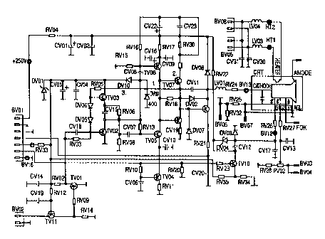
Fig. 1 shows the amplifier stage 1 with the transistors
TV06 and TV05, as well as the emitter follower 2 with the
transistor TV07 and the driver stage 3 with the transistor TV03
D 93/034A
3
and the resistors RV05 and RV03, which provide the overall
amplification. The transistor TV05 receives from the transistor
TV03 c.c. and d.c. voltage information, whereas the transistor
TV06 receives on1_y the c.c. voltage information. The circuit
takes the controlled variable from the transistor TV07 of the
emitter follower 2, from the current path of the latter. The
frequency dependence in the form of a controlled variable is
produced by the voltage drop across the resistor RV30, since at
high frequencies the reactive current of the transistor
increases as a physically dependent consequence. The voltage
consequently increases, and at the input of the amplifier stage
1 the operating point is influenced in the desired way. The
capacitor CV23 serves as a filter and the capacitor CV22 serves
as a rectifier. That means that they suppress the remaining
high-frequency and video components. This voltage is fed to the
transistor TV06 via the resistor RV16. The basic setting is
performed by means of the resistors RV15 and RV16. This setting
may be chosen to be very economical in the current drawn. The
quiescent current is determined furthermore by the transistor
TV07 and the load is determined by the resistor RV05.
Fig. 2 shows a further exemplary embodiment. To
compensate for the influence of the resistor RV05, an additional
control is possible by means of RV16. If the brightness
controller were used to run through the signal voltage over the
full d.c. range, a voltage drop would be produced across the
resistor RV30 without a high frequency being used, and the
control would load the resistor RV05 and the transistor TV07.
This is avoided by the resistor RV15 being connected via the
point A to the resistor RV05. Tf the d.c. voltage then increases
at point A, this is additionally evaluated as a control
component from the base of the transistor TV06. If the d.c.
voltage increases without a high frequency being required, it is
avoided that the operating current becomes too great.
Fig. 3 shows a further exemplary embodiment of the
invention. This exemplary embodiment has as a protective measure
a diode DV11, in order that the transistor TV06 does not receive
an excessive base current if the resistors RV30 and/or RV31 are
removed. Furthermore, the diode DV11 also protects against an
excessive increase in the control voltage at the amplifier
D 93/034A
~~~;~~~~
4
stage. The diode DV12 serves for compensation of the base-
emitter diode of the transistor TV06, in particular for
temperature compensation. The resistor RV31 serves for
intensification of the filtering of the capacitor CV22.
Fig. 4 shows a simplified equivalent circuit diagram.
The voltage picked off across the resistor RV30 is passed on via
the high-pass filter 4 and the resistor RV16 to the transistor
TV06. The transistor TV06 is in turn connected to the emitter
follower TV07. The high-pass filter comprises the capacitor CHP,
the diodes D1, D2, the filter capacitor CF and the load resistor
RA. If a higher signal current is required on account of the
increasing frequency, an increasing of the signal current can be
performed on account of the return via the high-pass filter 4 to
the base of the transistor TV06.
Fig. 5 shows the measurements in the case of a video
signal of 15 MHz.
Fig. 5.1 represents the video input signal at the
transistor TV01 with the characteristics white W, black S, burst
Bu and blanking B1.
Fig. 5.2 represents the video output signal VAUS at
BV13-CAT with control. With control, the output signal has a
maximum value of 230-Vpp. The maximum current requirement with
control is 120 mA.
Fig. 5.3 represents the video output signal VAUS at
BV13-CAT without control, the return signal s RS not being
adequately blanked. The maximum output signal VAUS is limited
and distorted. Without control, the output signal has a maximum
value of 50 Vpp. The maximum current requirement without control
is about 60 mA.
The same overall quiescent current of the output stage
of 13 mA at the operating voltage UB=250 volts applies for both
values, with or without control. That corresponds to a power of
3.25 watts. The maximum current requirement without control is
about 60 mA and with control is 120 mA. Since these values occur
only briefly, the overall situation is positive with respect to
outlay and power consumption.
Each transistor has a transition frequency, at which the
amplification of high frequency HF reaches the value 1. The
absolute limit of this transistor with respect to HF
D 93/03~A
amplification is then reached. This value "1" is also referred
to as the "gain bandwidth product". At the operating point of
the maximum transition frequency, a transistor can also deliver
the highest peak output level for high frequency. This operating
point is associated with a higher current consumption.
In Fig. 6 this higher current consumption is represented
by the change from the operating point AP1 to the operating
point AP2 due to the increasing of the current ic. For the
design of the amplifier it is very important whether it is
operated with a power loss of 1 W or 10 W, since the cooling
surfaces, the high-frequency channel and the mains power unit
have to be of a larger design.
Fig. 7 shows a further development of the invention. The
amplification is determined by a negative voltage feedback in
the usual sense due to the ratio of the resistors RV03 and RV05.
The voltage amplification of the circuit is governed by the
transistors TV05 and TV06. The transistor TV06 is represented
here as a controlled current source. It thus acts as a load
resistance for the transistor TV05 and ensures a high
amplification factor. The high frequency is fed via the
capacitor CVOB. The increasing of the transition frequency of
the transistors TV06 and TV05 takes place due to the d.c.
voltage which occurs across the resistor RV17 and CV09. The
collector current of the transistor TV06 is increased and
consequently so too is the transition frequency. As represented
in Fig. 6, the operating point AP1 shifts to the operating point
AP2. Depending on demand, there are also intermediate values. In
order to maintain symmetrical driving, the correct operating
point for the transistor TV05 is then reset by means of the
resistors RV05 and RV03. The transistor TV05 then operates in
the same way with a higher current.
Consequently, its transition frequency has then also
been increased. Usually complementary types are used for the
transistors TV05 and TV06. Consequently, the d.c. voltage
amplification is symmetrical and high up to the highest
frequencies. Since this case only occurs with specific signals,
the designing of the cooling and of the mains power unit can be
simplified.
If the high-frequency operating point is improved by
D 93/034A
6
increasing the current in the transistor stages TV05 and TV06,
this simultaneously ensures stabilization of the circuit. The
transistor TV07 then only continues to supply control current if
it is offered sufficient high frequency. This ensures that it
does not become possible to over-control the overall circuit. If
the transistor TV06, and consequently also the transistor TV05,
is opened beyond the optimum, the high-frequency amplitude drops
again, and the control current no longer increases. Therefore,
this circuit remains automatically at the maximum value - the
optimum for high frequency. Increases in d.c. voltage are
corrected by means of negative-feedback resistors RV03 and RV05.
Consequently, only operation between the compromise minimum for
the video signal and the high-frequency optimum is possible.
Fig. 8 shows that the frequency spectrum in the upper
range is really only driven to high output levels in the case of
particular signals. Fig. 8.1 shows the video signal V and Fig.
8.2 shows the test signal T.
The improvement in modulation is represented in Fig. 9.
The maximum output voltage max. A is represented in dependence
on the frequency F in the case without control oR and with
control mR.
The following components were used in the case of a
circuittested:
TV03 BF 763 RV03 820 S2 CV09 10
nF
TV05 2SC3790 RV05 33 kS2 CV16 4.7
~,F
TV06 2SA1480 RV15 150 kSZ/180 CV22 47
kSZ ~,F
TV07 2SC3790 RV16 1 kS2 CV23 10
nF
DV11 ZPY6.2 RV17 100 S2
DV12 1N4004 RV30 150 S2
RV31 1 kS2