Note: Descriptions are shown in the official language in which they were submitted.
2 i 26394
SCANNABLE INTERFACE TO NON-SCANNABLE MICROPROCESSOR
BACKGROUND OF THE INVENTION
The present invention relates to the field of
digital processing systems with diagnostics capabilities.
More specifically, in one embodiment, the invention provldes
a means for scanning scannable processor circuitry without
disturbing a nonscannable microprocessor which forms part of
a digital system.
To fully diagnose a logic-only circuit (i.e., no
memory of past states), a diagnostic system need only control
the overall inputs to the circuit, and record the outputs.
The outputs for a known set of inputs, when compared to an
expected set of outputs, will indicate whether the circuit is
working properly. Circuits with memory elements, such as
flip-flops, latches, and memory storage cells, are more
complicated to dlagnose.
To fully diagnose circuits with memory elements,
not only must the inputs be controlled, but the internally
remembered states must be known and controllable. Some
internal states can be controlled by manipulation of the
inputs to the circuit. For example, the internal state of a
counter, i.e., its count, can be controlled by asserting a
reset input of the counter to reach a known state, then
clocking the clock input to reach the desired internal state.
Thls, of course, ls not practical with today's complex
circuits. Furthermore, for certain tests, the internal state
might need to be set to a state whlch is not reachable
A 64157-430
21 263~4
through mere manipulatlon of the clrcult's lnputs.
What ls needed is a means for reading the lnternal
state of the circult and for settlng the lnternal state to a
speclflc state. Wlth dlscrete clrcultry, an lnternal state
can be read by problng each memory element and a known state
can be set by gatlng off each memory element output and
substltutlng a loglc value conslstent with the deslred
lnternal state. Wlth lntegrated clrcultry, however, the
number of plns over whlch slgnals can be communlcated between
a test system and the lntegrated clrcult severely llmlts the
number of plns whlch can be allocated to lnternal state
testlng and control.
One well-known method of deallng wlth dlagnostlcs
ln lntegrated clrcults ~IC's) ls to lnclude a scan path among
the loglc of the clrcult. A scan path ls a serlal path
llnklng all the memory elements of a clrcult, or at least
those whlch are to be scannable elements, lnto a serlal
stream. Placlng the elements ln a serlal scan path allows
the lnternal state to be read serlally from one pln, and
allows the lnternal state to be set wlth one pln.
The lntegrated clrcult has a mechanlsm for
swltchlng from a normal clrcult operatlon mode to a test
mode. In the normal clrcult operatlon mode, a memory element
ls responslve to lts lnputs, and ln a test mode, the memory
element ls responslve to data passlng along the scan path.
Consequently, shlftlng data lnto and out of the scan path
wlll cause the outputs of the memory element to change as the
data shlfts by. If the memory element ls one whlch dlrectly
A 64157430
- 2126394
-- 3--
affects the output of the circuit, the shifting of test data
on the scan path will appear as data rippling over the
outputs of the circuit.
To set the circuit to a known state (scan in),
setting for each memory element in the scan path are scanned
into a scan lnput, and to read the state of the clrcuit (scan
out), data is read from a scan path output. The scan in and
scan out is performed by clocking the scan path by a number
of clocks equal to the number of memory elements ln the scan
path. Of course, a scan enable must be provided, which when
not asserted allows for normal operation of the circuit.
Thus, in normal operation, the circuit behaves as designed,
and when the scan enable is asserted, the circuit behaves as
a serial register encompassing all the diagnosable memory
elements.
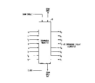
Fig. 1 illustrates thls concept. Fig. 1 shows a
parallel reglster 10, with 8 bits of data input, 8 bits of
data output, a clock input, an input for a scan enable
signal, a scan data input, and a scan data output. Register
ZO 10 operates as a register when the scan enable signal is not
asserted, wlth data passlng from the lnputs Io-I7 to the
outputs 00-07 wlth the clock.
When a scan enable slgnal is asserted, the data
inputs no longer affect the data outputs. Instead, the data
outputs are affected by the data scanned lnto the reglster
via the scan data input using the clock. The current
lnternal state of reglster 10 ls read out at the scan data
output. Thls scanning process presents a problem where
A 64157-430
~1 26394
-- 4--
reglster 10 ls part of a larger system. Suppose reglster 10
contains all zeros, and "10000000" ls to be scanned ln, where
the "1" ls to end up as blt 7. Because the scan lnput ls
coupled to blt 0, the "1" wlll rlpple through each of the
outputs as lt ls belng clocked ln, thus dlsturblng any
clrcult element whlch depends on the output of reglster 10,
thereby dlsturblng the states of other clrcults.
One solutlon to the problem of output rlppllng of
reglster 10 ls to place another 8-blt nonscannable latch at
the output of reglster 10, and not clock that latch whlle a
scan ls occurrlng, thus shleldlng any dependent clrcult
elements from reglster 10. However, thls leaves no way of
testlng the now-added nonscannable latch.
Another solutlon ls to coordlnate the scan of
reglster 10 wlth the scan of the dependent elements.
However, where the dependent elements are not scannable, such
as where the dependent element ls an enclosed IC provlded by
another manufacturer, thls solutlon ls not posslble.
From the above lt ls seen that an lmproved means ls
needed for scannlng a clrcult whlch has dependencles ln a
nonscannable clrcult, such as a mlcroprocessor, wlthout
dlsturblng the operatlon of those dependent clrcults.
SUMMARY OF THE INVENTION
An lmproved clrcult dlagnostlc system ls provlded
by the present lnventlon.
In one embodlment of a diagnostlc system accordlng
to the present lnventlon, the dlagnostlc system can scan
everythlng up to the boundary of a nonscannable clrcult
64157-430
CA 02126394 1998-0~-12
-- 5 --
element, without disturbing the nonscannable element. One such
diagnostic system for a digital computer is a processor board
comprising scannable processor ASIC's (Application Specific
Integrated Circuits), including a processor interface chip
(PIC), which interfaces a nonscannable microprocessor and the
other scannable processor ASIC's with a processor bus between
the microprocessor and the PIC. A scan controller is provided
which reads and writes scan data through the scannable ASIC's,
including the PIC. The ASIC's are typically individual chips
on a processor board, with each chip having a separately
controllable scan path. However, in alternate embodiments,
more than one ASIC might be combined on a single chip, or reduce
space more than one chip might make up a single ASIC. Also, the
processor circuitry need not be on a single board.
In particular embodiments, the scan controller is
itself an ASIC, a Maintenance and Diagnostic Chip (MDC), which
makes requests of the PIC to bus step the microprocessor. When
the MDC requests a bus step, the microprocessor and the
processor ASIC's run normally, until the PIC determines that
the microprocessor can be held up and that the PIC can be
scanned without violating the bus protocol. At that point, the
microprocessor is held up, waiting for a response from the PIC.
Because the microprocessor is expecting the wait, a delay in
getting the response will not necessarily affect the state of
the microprocessor.
In accordance with the present invention, there is
provided a diagnostic system for diagnosing states of circuit
64157-430
CA 02126394 1998-0~-12
- 5a ~
elements within a digital computer where internal states of a
microprocessor in the digital computer are not available for
control by the diagnostic system, comprising: a plurality of
- scannable processor circuits; a processor interface circuit
coupled to the microprocessor via a processor bus and coupled
to said plurality of scannable processor circuits via an
internal bus, wherein said processor interface circuit inter-
faces with the microprocessor using a predetermined bus
protocol over said processor bus; a scan controller coupled to
said plurality of scannable processor circuits and said
processor interface circuit, wherein said scan controller is
capable of reading out and modifying internal states of said
plurality of scannable processor circuits and said processor
interface circuit; a first signal means for providing a
maintenance request signal from said scan controller to said
processor interface circuit; a second signal means for provid-
ing a maintenance approval signal from said processor interface
circuit to said scan controller; and means within said
processor interface circuit and coupled to said processor bus,
for ensuring that said maintenance approval signal is not
asserted if said predetermined bus protocol would be violated
by a change of an internal state of said processor interface
circuit.
In accordance with another aspect of the invention,
there is provided a method of diagnosing scannable circuit
elements which are coupled in a circuit including unscannable
circuit elements, comprising the steps of: isolating the
64157-430
CA 02126394 1998-0~-12
- 5b -
unscannable circuit elements from the scannable elements over a
known interface, said known interface connecting the unscannable
circuit elements to a scannable interface element; asserting a
first signal requesting a diagnostic, where said first signal
is input to said scannable interface element; waiting for any
in-process bus cycles to complete over said known interface;
holding control signals output by said scannable interface
element over said known interface in a fixed state, said fixed
state selected such that a state of the unscannable circuit
elements is not uncontrollably affected by any unfixed signals
on said known interface while said scannable interface element
is being scanned.
In accordance with a further aspect of the invention,
there is provided a digital processor system with scannable
processor circuits and a nonscannable microprocessor, compris-
ing: a processor bus which uses a predefined bus protocol and
predefined handshaking sequences comprising bus steps to couple
the microprocessor to the scannable processor circuits; a
scannable processor interface circuit coupled to said processor
bus, said scannable processor interface circuit including logic
circuitry which allows said scannable processor interface
circuit to perform a bus step of the processor; a first logical
circuit coupled to said scannable processor interface circuit,
which performs a bus step of the processor bus such that said
scannable processor circuits can be scanned between bus steps
without violating said bus protocol; a second logical circuit,
coupled to the scannable processor circuits for single-stepping
64157-430
CA 02126394 1998-0~-12
at least one of the scannable circuits; and a third logical
circuit, coupled to the first and second logical circuits,
which allows said first and second logical circuits to be
included in a scan path through the scannable processor
circuits.
One advantage of the present invention is that the
processor board, up to the processor bus, can be scanned with-
out disturbing the state of the microprocessor. This is
useful where a computer system including a nonscannable micro-
processor needs to be tested, set into a known state, ordebugged in a setting closely aligned with a normal operation
setting.
Another advantage of the present invention is that
it also allows for the processor board to be bus stepped
without requiring any special hardware in the microprocessor.
If no special hardware is needed, then a standard microprocessor
chip could be used.
Yet another advantage of the present invention is
that it allows clock cycle single stepping of the scannable
ASIC's without interference from the microprocessor. Some
diagnostics can be run even without the presence of the
microprocessor.
A further understanding of the nature and advantages
of the invention herein may be realized by reference to the
remaining portions of the specification and the attached
drawings.
64157-430
CA 02126394 1998-0~-12
- 5d -
BRIEF DESCRIPTION OF THE DRAWINGS
Fig. 1 is a block diagram of a typical scannable
register;
Fig. 2 is a block diagram of a digital computer with
a nonscannable microprocessor and processor circuitry;
Fig. 3 is a state diagram of a protocol between a
PIC and an MDC for performing scans or processor bus steps
without disturbing the operation of a microprocessor on the
processor bus;
Fig. 4 is a block diagram of an output enable latch
circuit and a processor bus handshake signal register circuit
according to the present invention; and
Fig. 5 is a block diagram of the PIC showing
diagnostic state machines.
DESCRIPTION OF THE PREFERRED EMBODIMENTS
Fig. 2 is a block diagram of a digital computer
system 20 with a nonscannable microprocessor 22 and scannable
processor circuitry 24 on a processor board 21. Processor
circuitry 24 includes a variety of ASIC's such as a processor
interface chip (PIC) 30, a memory interface chip (MIC) 32,
interprocessor bus controllers 34x,y (IPBX/IPBY), input/output
controller system (IOS) 36 and a maintenance and diagnostic
chip (MDC) 38. Processor circuitry 24 is interconnected by
three busses, an internal bus (IBus) 40, a maintenance bus
(MBus) 42, and an external bus (EBus) 43. Processor circuitry
24 is shown in Fig. 2 interfacing to a memory 44 via the MIC,
to other processing units 46x,y via interprocessor controllers
64157-430
CA 02126394 1998-0~-14
34x,y, and to I/O devices 48 via IOS 36 and Ebus 43. PIC 30
includes state machines, shown in more detail in Fig. 5, whose
operation is discussed in connection with Figs. 3 and 5.
The Mbus contains signal lines for controlling the
scan of the ASIC's attached to the Mbus, allowing the MDC to
set up an ASIC for a scan operation or to hold its state in
place. Holding the state of one ASIC in place allows the MDC
to scan another ASIC without disturbing the state of the held
ASIC. The Mbus also contains scan data lines used for writing
scan data into an ASIC and for reading scan data out of an ASIC.
In addition to the Mbus, the MDC interfaces with the
PIC over three lines, DIAG_REQ, STEP_REQ, and DIAG_OK, although
in some embodiments, the information provided by these signals
is distributed over a different set of signal lines.
In the normal operation mode of digital computer
system 20, the Mbus is not needed. Microprocessor 22 issues
requests to the PIC over a processor bus (PBus) 50, which in
turn relays the requests over the IBus to other ASIC's. For
example, if microprocessor 22 requests a memory write, the
request will include the data to be written and will be passed
from the PIC to the MIC for storage of the data accompanying
the request into memory 44. Similarly, a read request for a
given block of memory 44 is sent from microprocessor 22 over
the PBus to the PIC, and then from there to the MIC over IBus
40. In response, the MIC retrieves the data from memory 44
and passes it to the PIC, which relays it to microprocessor 22
at the appropriate time in the PBus protocol.
64157-430
CA 02126394 1998-0~-14
- 6a ~
In a diagnostic mode, the MDC can control the ASIC's
over the Mbus. Although the Mbus is shown leading to each ASIC
individually, in some embodiments, the scan path through the
ASIC's is serial, i. e., all the scan data runs through each
ASIC. The latter configuration is useful where a connection
between two ASIC's is less costly than the connections from
each ASIC to the MDC.
One means for controlling diagnostics of an ASIC,
such as MIC 32, for example, is by scanning a desired state
64157-430
21 26394
lnto the ASIC, over the MBus. Because each ASIC wlthin
processor clrcultry 24 ls scannable, the state of the ASIC
can be monltored and changed. Therefore, the MDC need not be
concerned wlth the lnternal operatlon of the ASIC's
lnteractlng on the IBus slnce the states of all scannable
ASIC's can be scanned in or held. For example, durlng a scan
operatlon, the MIC can be scanned ln such a way that the
rlppllng of the scan blts appears on the IBus, but thls ls
not a problem lf each ASIC on the IBus ls also under the
control of the MDC.
Generally, when an ASIC ls belng scanned, the
abllity of the lnputs to the ASIC to affect the state of the
clrcultry lnslde the ASIC ls blocked. In the case where all
the ASIC's are coupled on a serlal scan path, when one ASIC
ls scanned, they are all scanned, so the effect of the
rlppllng of the scan blts on the IBus ls of llttle concern.
In the case where each ASIC has a scan path dlrectly
connected to the MDC, the MDC can lssue a hold command over
the MBus to all ASIC's whlch are not belng scanned, to
prevent the rlppllng on the IBus from trlggerlng an
undeslrable input to the unscanned ASIC's. In summary,
because the ASIC and lts surroundlng envlronment ls fully
controllable by the MDC, the MBus ls all that ls needed
between the MDC and that ASIC. The exceptlon to thls rule,
shown ln Flg. 2, ls PIC 30, whlch has an lnterface to
mlcroprocessor 22, whlch ls not controllable by MDC 38.
The PIC ls freely scannable by the MDC wlthout
regard to the status of the PBus, except for memory elements
~ 64157-430
2 1 263~4
--8
whlch would affect the slgnals put out on the PBus, but even
those memory elements are scannable when provlded wlth the
control loglc embodled ln the state dlagram shown ln Flg. 3.
These slgnals comprlse M address/data lines and K control
llnes for a total of N llnes. In one embodlment, 6 control
lines (Kz6) and 82 address/data llnes (M=82; N=88). These
llnes are shown ln greater detall ln Flg. 4. When certaln
condltlons are met, mlcroprocessor 22 wlll not be affected by
the slgnals on the address/data llnes. These condltlons are
met when control slgnals passed from the PIC to the
mlcroprocessor lndlcate that the data on the address/data
llnes ls not valld. Another such condltlon ls when
mlcroprocessor 22 ls waltlng for a response to a
mlcroprocessor request and a "response ready" slgnal from the
PIC to the mlcroprocessor has not yet been asserted by the
PIC. Thus, the MDC must assure that the PBus ls ln a
condltlon such that a scan can occur wlthout causlng
undeslred operatlon of mlcroprocessor 22.
Flg. 3 ls a state dlagram showlng the varlous
protocol states between the MDC and the PIC. The state ls
tracked by a state machlne 52 (see Flg. 5) wlthln the PIC,
although other conflguratlons are posslble. Slgnlflcantly,
even thls state machlne 52 ls scannable.
Flg. 5 shows PIC 30 ln greater detall. PIC
lncludes state machlnes 52, 54, 56. Slgnal connectlons are
provlded for state machlne 52 to send a stay_off_PBus slgnal
to PBus stàte machlne 54 and a stay_off_IBus slgnal to IBus
state machlne 56, as well as slgnal connectlons for recelpt
64157-430
AL
.L~"
3 q 4
g
by state machlne 52 of a PBus_ldle slgnal from PBus state
machlne 54 and an IBUS_ldle slgnal from IBus state machlne
56.
In state 1, the PIC and the MDC are ln the normal
operatlng mode. The state machlne 52 changes from state 1 to
state 2 when the DIAG_REQ slgnal ls asserted. Throughout
thls descrlption, the slgnal may be lnterchangeably referred
to as an "asserted" slgnal or a slgnal wlth a value of
"true", wlth the opposltes belng a "deasserted" slgnal and a
slgnal wlth a value of "false". The DIAG_REQ slgnal ls
asserted by the MDC when a scan of the PIC, a bus-step of the
PBus or a slngle clock cycle step of the clock of processor
clrcultry 24 ls deslred.
Upon changlng to state 2, the PIC deasserts a RDY
(ready) slgnal. The RDY slgnal represents two slgnals, RdRdy
(read ready) and WrRdy (wrlte ready), but for clarlty, slnce
the slgnals are treated ldentlcally wlthln state machlne 52,
they are shown ln Flg. 3 as a slngle slgnal. These slgnals,
RdRdy and WrRdy are output by the PIC over the PBus, and are
lnput by mlcroprocessor 22. Another slgnal, stay_off_bus, ls
asserted each clock cycle ln whlch the state remalns state 2.
As wlth the RDY slgnal, the stay_off_bus slgnal also
represents two slmllarly treated slgnals, a stay_off_PBus and
a stay_off_IBus slgnal, whlch are output by state machlne 52
to state machlne 54 and 56 (see Flg. 5). State machlne 52
remalns ln state 2 untll both the PBus and the IBus are ldle
wlth re~pect to the PIC, at whlch polnt state machlne 52
changes to state 3.
~A 6415
7-430
2 1 26394
-9a-
The stay_off_bus signal is sent to state machines
54, 56, and state machine 52 stays in state 2 until it
receives a bus idle signal from both state machines 54, 56.
Upon changing to state 3, the PIC asserts the
DIAG_OK signal, which indicates to the MDC that stepping and
scanning are allowed. State machlne 52 remalns in state 3
until either the MDC deasserts DIAG_REQ or the MDC asserts
the STEP_REQ slgnal. If the MDC deasserts the DIAG_REQ
slgnal, state machine 52 changes to state 1, and the flow for
a scan operation ls completed. Upon changlng to state 1, the
PIC asserts RDY (RdRdy, WrRdy) and deasserts stay_off_bus.
On the other hand, lf the MDC malntalns the
DIAG_REQ signal asserted and asserts the STEP_REQ signal, the
state machlne changes to state 4, to begln a single bus step
of the PBus. Upon changlng to state 4, the PIC asserts the
RDY slgnal, and walts ln state 4 untll a mlcroprocessor
request occurs. Because the bus step runs untll the next
processor request occurs, lt ls not a slngle step of the
mlcroprocessor clock, but ls rather a slngle block of code
between two requests. Of course, wlth some mlcroprocessors,
a request for an lnstructlon occurs each instruction cycle,
but in a preferred embodiment, microprocessor 22 malntalns a
secondary cache for caching instructions and recently used
data, making it possible to run for several instruction
cycles without needing to interact with the PIC.
State machine 52 remains ln state 4 untll the PIC
has accepted the microprocessor request, and then changes to
state 5. Upon changing to state 5, the PIC asserts DIAG_OK
~A 6
4157-430
21 263'~4
-9b-
lf DIAG_REQ ls stlll true, and also deasserts RDY. Thls
causes mlcroprocessor 22 elther to walt for the results of
the request, or to continue lnternal processlng ~such as
readlng
~A 6415
7-430
21~6~
-- 10
instructions from its primary or secondary cache). Either
way, the PBus is not used.
The state machine remains in state 5 until the MDC
either deasserts DIAG_REQ or asserts STEP_REQ. In either
case, the state transitions are from state 5 to state 6, and
then to state 3. From state 3, if the signals from the MDC
have not changed, the former case causes a transition to state
1, and the latter to state 4.
Upon entering state 6, the PIC deasserts the
stay_off_bus signal, to allow the request to be processed by
processor circuitry 24. State machine 52 remains in state 6
until the request processing is complete and a response is
sent to microprocessor Z2, and then transitions to state 3.
Upon the transition to state 3, the PIC once again asserts
stay_off bus and asserts DIAG OK for one clock cycle if_
DIAG_REQ is still true.
Thus, according to the state diagram shown in Fig.
3, the PIC and the MDC can coordinate times for scanning
processor circuitry 24, including the PIC itself, and for bus
stepping microprocessor 22 and PBus 50, without microprocessor
22 even being aware of what is happening. This eliminates the
need for modifications to microprocessor 22. But one benefit
of such an arrangement is that microprocessor 22 could be
selected from available microprocessors without limiting the
selection to those microprocessors which are scannable. In
one embodiment, microprocessor 22 is two R4400 microprocessors
(manufactured by the MTI division of Silicon Graphics, Inc.)
operating in tandem.
Of course, if the PIC is fully scannable, then the
ripple of a scan appearing on some control lines of the PBus
might still affect microprocessor 22. For example, if a flip-
flop normally outputs a value for the RDY signal, when the
scan path running through that flip-flop is scanned, the RDY
output will ripple in the pattern of the bits of the memory
elements in the scan path. Thus, to avoid undesirable
operations, some memory elements cannot be directly connected
to the PBus. However, some means is needed to test these
memory elements.
212533 l
11
Table 1 shows several signals which are output by
the PIC onto the PBus which must be held during a scan ("*"
indicates that a signal is active low).
Signal Value
ValidIn* False
ExtRqust* False
RdRdy* False
WrRdy* False
IvdAck* True
IvdErr* False
Table 1.
ValidIn* is a PBus line on which the PIC indicates
that the data driven onto the PBus by the PIC is valid.
ExtRqust* is a PBus line on which the PIC sends a request to
the microprocessor. RdRdy* and WrRdy* were previously
discussed. InvAck* and InvErr* are PBus lines on which the
PIC indicates the successful and unsuccessful completion,
respectively, of an invalidate/update request made by the
mlcroprocessor.
During a scan operation, the PIC must maintain the
~ ~d tus oE these bit lines, since the signals on these lines
are part of the PBus handshaking protocol between the
microprocessor and the PIC. However, it is not enough to
merely leave out of the scan path any memory elements which
affect these lines, as that would preclude diagnostics which
read or write these lines.
Fig. 4 illustrates how the PIC is made fully
scannable, while at the same time providing fixed outputs
during a scan when necessary. Fig. 4 shows a one-bit memory
element 80, an N-bit memory element 82, an M-bit latch 84, a
K-bit 2-to-1 multiplexer 86, an invertor 90, and an N output
driver 92. The actual configuration may vary from embodiment
to embodiment, but the essential features are the same. For
example, memory element 82 is shown for clarity as a single
device, where in some PIC's, the functionality of memory
element 82 is distributed throughout the PIC.
In the example of Fig. 4, an output enable signal
which is output during normal operation of the PIC is output
2 1263"~ ~
- 12
from memory element 80 to latch 84, which outputs its inputs
to an enable input of output driver 92, when a signal applied
at an enable (E) input of latch 84 is low (active). N signals
are output from memory element 82 to either multiplexer 86 (X
s signals) or directly to output driver 92 (M signals). The K
signals going to multiplexer 86 are control lines coupled to
the PBus when a select signal is not asserted (i.e., false, or
"0") at a select (S) input to multiplexer 86. When the E
input to latch 84 is false, latch 84 latches its input to its
output, and when the S input to multiplexer 86 is asserted
(select input set to "1"), multiplexer 86 inputs a preselected
set of constants from its "1" input and outputs them onto the
K control lines of the PBus.
The use of the circuitry shown in Fig. 4 will now be
described. During a scan operation, the PBus should not be
affected. Therefore, any PBus line which is being driven
during a scan should be one of the K lines output by
multiplexer 86. The K signals shown in Table 1 are examples
of signals which are always the same value during a scan.
Thus, the first column of Table 1 lists some signals which
wo~id be part of the K lines from memory element 82 to the "o"
input of multiplexer 86, and the second column shows the
constants which would be applied to the "1" input of
multiplexer 86.
Within the PIC, at least one memory element (a flip-
flop) maintains a bit indicating whether or not the PIC is the
current PBus master. For illustration purposes, assume that
this bit is stored in memory element 80. When a scan begins,
the scan signal line is set true, causing the E input to latch
84 to go false, which latches the bit onto line 94 which
connects to the enable input of output driver 92. By the way,
the enable input might fan out to each bit of output driver
92. Also, the K constant bits are output onto the PBus.
With the configuration shown in Fig. 4, all memory
elements of the PIC are scannable, except for latch 84. This
should not be a problem, since latch 84, when a scan is being
performed, merely reflects the contents of memory element 80.
Note that memory element 80 and 82 are scannable. Fig. 4
. . CA 02126394 1998-0~-14
- 13 -
shows them on the scan path. The scan path runs from the Mbus
through each memory element on the scan path, where memory
elements 80 and 82 can be anywhere along the scan path. Also,
to be fully scannable, the state machine 52, itself, is also
scannable, since it contains at least three bits of memory to
remember the current state, which is one of six values.
The above description is illustrative and not
restrictive. Many variations of the invention will become
apparent to those of skill in the art upon review of this
disclosure. The scope of the invention should, therefore, be
determined not with reference to the above description, but
instead should be determined with reference to the appended
claims along with their full scope of equivalents.
64157-430