Note: Descriptions are shown in the official language in which they were submitted.
WO 93/13602
fCI'/SE92f00~09
1
Shifting the phase of a clock signal in particular for
clock recovery of a diclital data signal.
Technical area.
According to a first aspect the present invention relates
more generally to a system for shifting the phase of a clock
signal, including first means for receiving said clock signal
DLO and providing a number of auxiliary clock signals phase
shifted with respect to said clock signal and to each other,
second means for choosing two of the auxiliary clock signals
between the phases of which a desired new phase of said clock
signal is situated, and third means fox. mixing the two chosen
auxiliary clock signals with each other until a signal with
said desired phase is obtained.
According to a second aspect the inventian relates to
a method for clock recovery of a digital data signal,
wherein a number of mutually phase shifted auxiliary clock
signals are used to create a recovered clock signal for the
data signal based upon the result of detection of a phase
position error, if any, between the data signal and its
rec~ve~ed clock signal, and
a.system for Block recovery .of a digital data signal
including a phase detector for receiving the data signal. ands
transmitting the same after clock recover, a phase
correcting device for creating and emitting, by means of a
number of mutually phase shifted auxiliary signals derived
from an incoming clock signal, a recovered clock signal for
3~ the data signal, said recovered clock signal being fed to the
phase detector for detecting a phase position error, if any,
between the data signal and its recovered clock signal and to
transmit information with respect to this to the phase
correcting device.
:Mate of the art.
Among conventional methods for providing clock recovery
can be mentioned the use of so called SAw filters, or a
voltaCde or cuY°rent controlled oscillator o ~Th~sP ~n1 gafi-_i ~ns
WO 93/i364o2 ~ PCf/Si:921~08419
have the following disadvantages.
SAW filters are relatively expensive, space consuming,
cannot be integrated and consume a relatively large amount of
power. Furthermore, one filter is required for each input.
A controlled oscillator can certainly be integrated,
except for ttie crystal, but requires a relatively great
amount of electronic circuitry for carrying through the
control, and consumes a relatively large amount of power.
Through U.s. ~ 955 p~0 a digital clock recovery system is
20 knorom, which includes a phase sensor for a digital data
signal. The phase sensor provides information to a p&~ase
correcting device with regard to the phase position of the
digital data signal and obtains therefrom a first auxiliary
data clock signal being the recovered clock of the digital
15~ signal, as well as a second auxiliary data clock signal which
has a defined phase difference with respect to the first one.
The phase sensor compares the phase relation between the
active edges of the pulses of the digital data signal and the
a~econd auxiliary data signal. If the result of the comparison
20 is that no phase difference can be seen, a correction signal
is generated which causes a phase correction of the two
auxiliary data clock signals resulting in the creation of the
defined phase difference.
xn U8 ~6 2~.a 77?. a controlled phase shift circuit is
25 described. The phase of the clock pulses is continuously
optim~.~ed with respect to the received signal under the
control of pseudo-error detectors.
In ~P 60-X53.74~ it is described how optimal timing of
sampling as always maintained by the use of a timing
30 synchroni~a.ng system including a variable phase circuit
automatically controlling/regulating 'the phase of an output
signal from an osoilla~tor forming an original oscillator for
a timing signal.
zn ~F fil.-~1953~ a digital phase synchronising circuit. is
35 described. The phase of the output clock signal of the
circuit is corrected and its phase locking properties are
improved by detection of the magnitude of the phase shift in
either direction.of the output clock signal based upon .an
iniaut clock signal, and proportional settincx of the ~ahase
CA 02126552 2000-10-23
3
correction with respect to the detected magnitude.
Statement of Invention
A first object of the invention is to provide a system
in accordance with the first aspect, which allows simple and
continuous shifting of the phase of a clock signal.
A second object of the invention is to provide a method
and a system, of the kind defined by way of introduction
according to the second aspect, for clock recovery of a
digital data signal which can be integrated and, as compared
with conventional solutions, is cheaper and less power
consuming.
A further object of the present invention is to provide
a system for shifting the phase of a clock signal,
comprising: first means for receiving the clock signal and
providing a number of auxiliary clock signals phase shifted
with respect to the clock signal and to each other, second
means for choosing two of the auxiliary clock signals between
the phases of which a desired new phase of the clock signal
is situated, and third means for mixing the two chosen
auxiliary clock signals with each other until a signal with
the desired phase is obtained, including: a number of
controllable switching means having auxiliary clock signal
inputs for receiving the auxiliary clock signals, and a
common output on which the signal with the desired phase is
obtained, a control signal generator for providing a control
signal with a variable amplitude and sign, and a selector
circuit having a control input for receiving the control
signal, control outputs for controlling the switching means
to let through their respective auxiliary clock signals, and
activating means for monitoring the amplitude and sign of the
CA 02126552 2000-10-23
4
control signal and selectively activating a number of the
control outputs; wherein the activating means include an
analog control network and an analog selector, which both are
connected for receiving the control signal, the control
network controlling the selector for entirely opening, via
one of the chosen control outputs, a corresponding switching
means for letting through the corresponding auxiliary signal
without amplitude decrease, and for connecting, via another
chosen control output, the control signal with correct sign
to a corresponding switching means for letting through the
corresponding auxiliary clock signal with an amplitude
decrease determined by the amplitude of the control signal.
According to a further object of the present invention
there is provided a system for shifting the phase of a clock
signal, comprising: first means for receiving the clock
signal and providing a number of auxiliary clock signals
phase shifted with respect to the clock signal and to each
other, second means for choosing two of the auxiliary clock
signals between the phases of which a desired new phase of
the clock signal is situated, and third means for mixing the
two chosen auxiliary clock signals with each other until a
signal with the desired phase is obtained, including: a
number of controllable switching means having auxiliary clock
signal inputs for receiving the auxiliary clock signals, and
a common output on which the signal with the desired phase is
obtained, a control signal generator for providing a control
signal with a variable amplitude and sign, and a selector
circuit having a control input for receiving the control
signal, control outputs for controlling the switching means
to let through their respective auxiliary clock signals, and
activating means for monitoring the amplitude and sign of the
CA 02126552 2000-10-23
control signal and selectively activating a number of the
control outputs; wherein the controllable switching means
comprise a number of differentially connected pairs of first
and second controlled switches, the pairs being located
5 between voltage source means and a common differential output
having first and second terminals for forming the common
output for the signal with the-desired phase, the first and
second controlled switches of each pair having respective
outputs connected to the first and second terminals,
respectively, the pairs being further connected to the
voltage source means via current path means containing
current source means and control means connected to the
control outputs for controlling the current flow to the
pairs, the controlled switches having control inputs
connected for receiving the auxiliary clock signals.
According to a further object of the present invention
there is provided a system for shifting the phase of a clock
signal, comprising: first means for receiving the clock
signal and providing a number of auxiliary clock signals
phase shifted with respect to the clock signal and to each
other, second means for choosing two of the auxiliary clock
signals between the phases of which a desired new phase of
the clock signal is situated, and third means for mixing the
two chosen auxiliary clock signals with each other until a
signal with the desired phase is obtained, including: a
number of controllable switching means having auxiliary clock
signal inputs for receiving the auxiliary clock signals, and
a common output on which the signal with the desired phase is
obtained, a control signal generator for providing a control
signal with a variable amplitude and sign, and a selector
circuit having a control input for receiving the control
CA 02126552 2000-10-23
6
signal, control outputs for controlling the switching means
to let through their respective auxiliary clock signals, and
activating means for monitoring the amplitude and sign of the
control signal and selectively activating a number of the
control outputs; wherein the controllable switching means
comprise a number of sets of at least one differentially
connected pair each of first and second controlled switches,
the pairs being located between voltage source means and a
common differential output having first and second terminals
for forming the common output for the signal with the desired
phase, the first and second controlled switches of each pair
having respective outputs connected to the first and second
terminals, respectively, the sets of pairs being further
connected to the voltage source means via a number of
digitally controllable current sources having control inputs
connected to logic circuitry having as an input the control
signal with a variable amplitude and sign, and the controlled
switches having control inputs connected for receiving the
auxiliary clock signals.
According to a further aspect of the present invention,
there is provided a system for clock recovery of a digital
data signal, comprising: a phase detector for receiving the
data signal and transmitting the same after clock recovery, a
phase correcting device for creating and emitting, by means
of a number of mutually phase shifted auxiliary signals
derived from an incoming clock signal, a recovered clock
signal for the data signal, the recovered clock signal being
fed to the phase detector for detecting a phase position
error, if any, between the data signal and its recovered
clock signal and transmitting information with respect to
this to the phase correcting device, the phase correction
CA 02126552 2000-10-23
7
device including; a phase variation circuit for mixing, if
the phase position error is different from zero and the phase
position of the recovered clock signal is situated between
the phase position for two auxiliary clock signals, these two
auxiliary clock signals being mixed with each other for
forming an adjusted recovered clock signal having the same
phase position as the data signal; wherein the phase
variation circuit includes; a number of controllable
switching means for receiving on auxiliary clock signal
inputs the auxiliary clock signals and connected to a common
output, on which the recovered clock signal with the shifted
phase is obtained, and a selector circuit with control
outputs connected for controlling the switch means to let
through their respective auxiliary clock signals, and with
activating means for monitoring the magnitude and sign of the
control signal and selectively activating a number of the
control outputs; wherein the detector circuit creates and
transmits the phase position information in the form of an
analog signal, the amplitude of which is a measure of the
magnitude of the phase error, and the sign of which indicates
the direction of the phase error, and the activating means
include an analog control network and an analog selector,
which both are connected for receiving the analog signal, the
control network controlling the selector to entirely open,
via one of the two chosen control outputs, the corresponding
switching means for letting through the auxiliary clock
signal thereof without amplitude decrease, and to connect,
via the other chosen control output, the analog signal with
the correct sign to the corresponding switching means for
letting through the auxiliary clock signal thereof with an
CA 02126552 2000-10-23
8
amplitude decrease determined by the amplitude of the control
signal.
According to another aspect of the present invention
there is provided a system for clock recovery of a digital
S data signal, comprising: a phase detector for receiving the
data signal and transmitting the same after clock recovery, a
phase correcting device for creating and emitting, by means
of a number of mutually phase shifted auxiliary signals
derived from an incoming clock signal, a recovered clock
signal for the data signal, the recovered clock signal being
fed to the phase detector for detecting a phase position
error, if any, between the data signal and its recovered
clock signal and transmitting information with respect to
this to the phase correcting device, the phase correction
device including; a phase variation circuit for mixing, if
the phase position error is different from zero and the phase
position of the recovered clock signal is situated between
the phase position for two auxiliary clock signals, these two
auxiliary clock signals being mixed with each other for
forming an adjusted recovered clock signal having the same
phase position as the data signal; wherein the controllable
switching means comprise a number of differentially connected
pairs of first and second controlled switches, the pairs
being located between voltage source means and a common
differential output having first and second terminals for
forming the common output for the signal with the desired
phase, the first and second controlled switches of each pair
having respective outputs connected to the first and second
terminals, respectively, the pairs being further connected to
the voltage source means via current path means containing
current source means and control means connected to the
CA 02126552 2000-10-23
9
control outputs for controlling the current flow to the
pairs, the controlled switches having control inputs
connected for receiving the auxiliary clock signals.
According to a further aspect of the present invention
there is provided a system for clock recovery of a digital
data signal, comprising: a phase detector for receiving the
data signal and transmitting the same after clock recovery, a
phase correcting device for creating and emitting, by means
of a number of mutually phase shifted auxiliary signals
derived from an incoming clock signal a recovered clock
signal for the data signal, the recovered clock signal being
fed to the phase detector for detecting a phase position
error, if any, between the data signal and its recovered
clock signal and transmitting information with respect to
this to the phase correcting device, the phase correction
device including; a phase variation circuit for mixing, if
the phase position error is different from zero and the phase
position of the recovered clock signal is situated between
the phase position for two auxiliary clock signals, these two
auxiliary clock signals being mixed with each other for
forming an adjusted recovered clock wherein the phase
variation circuit includes; a number of controllable
switching means for receiving on auxiliary clock signal
inputs the auxiliary clock signals and connected to a common
output, on which the recovered clock signal with the shifted
phase is obtained, and a selector circuit with control
outputs connected for controlling the switch means to let
through their respective auxiliary clock signals, and with
activating means for monitoring the magnitude and sign of the
control signal and selectively activating a number of the
control outputs; wherein the controllable switching means
CA 02126552 2000-10-23
comprise a number of sets of at least one differentially
connected pair each of first and second controlled switches,
the pairs being located between voltage source means and a
common differential output having first and second terminals
5 for forming the common output for the signal with the desired
phase, the first and second controlled switches of each pair
having respective outputs connected to the first and second
terminals, respectively, the sets of pairs being further
connected to the voltage source means via a number of
10 digitally controllable current sources having control inputs'
connected to logic circuitry having as an input the control
signal with a variable amplitude and sign, and the controlled
switches having control inputs connected for receiving the
auxiliary clock signals.
According to another aspect of the present invention
there is provided a system for shifting the phase of a clock
signal, comprising: first means for receiving the clock
signal and providing a number of auxiliary clock signals
phase shifted with respect to the clock signal and to each
other, second means for choosing two of the auxiliary clock
signals between the phases of which a desired new phase of
the clock signal is situated, and third means for mixing the
two chosen auxiliary clock signals with each other until a
signal with the desired phase is obtained, including a number
of controllable switching means having auxiliary clock signal
inputs for receiving the auxiliary clock signals, and a
common output on which the signal with the desired phase is
obtained, means for providing control signals to the
switching means; wherein the controllable switching means
comprise a number of differentially connected pairs of first
and second controlled switches, the pairs being located
CA 02126552 2000-10-23
l0a
between voltage source means and a common differential output
having first and second terminals for forming the common
output for the signal with the desired phase, the first and
second controlled switches of each pair having respective
outputs connected to the first and second terminals,
respectively, the pairs being further connected to the
voltage source means via current path means containing
current source means and control means connected to the
control outputs for controlling the current flow to the
pairs, the controlled switches having control inputs
connected for receiving the auxiliary clock signals.
According to another aspect of the present invention
there is provided a system for shifting the phase of a clock
signal, comprising: first means for receiving the clock
signal and providing a number of auxiliary clock signals
phase shifted with respect to the clock signal and to each
other, second means for choosing two of the auxiliary clock
signals between the phases of which a desired new phase of
the clock signal is situated, and third means for mixing the
two chosen auxiliary clock signals with each other until a
signal with the desired phase is obtained, including a number
of controllable switching means having auxiliary clock signal
inputs for receiving the auxiliary clock signals, and a
common output on which the signal with the desired phase is
obtained, means for providing control signals to the
switching means; wherein the controllable switching means
comprise a number of sets of at least one differentially
connected pair each of first and second controlled switches,
the pairs being located between voltage source means and a
common differential output having first and second terminals
for forming the common output for the signal with the desired
CA 02126552 2000-10-23
lOb
phase, the first and second controlled switches of each pair
having respective outputs connected to the first and second
terminals, respectively, the sets of pairs being further
connected to the voltage source means via a number of
S digitally controllable current sources having control inputs
connected to logic circuitry, and the controlled switches
having control inputs connected for receiving the auxiliary
clock signals.
According to a further aspect of the present invention
there is provided a system for shifting the phase of a clock
signal, comprising: first means for receiving the clock
signal and providing a number of auxiliary clock signals
phase shifted with respect to the clock signal and to each
other, second means for choosing two of the auxiliary clock
signals between the phases of which a desired new phase of
the clock signal is situated, and third means for mixing the
two chosen auxiliary clock signals with each other until a
signal with the desired phase is obtained, including a number
of controllable switching means having auxiliary clock signal
inputs for receiving the auxiliary clock signals, and a
common output on which the signal with the desired phase is
obtained, means for providing control signals to the
switching means; wherein the controllable switching means
comprise a number of sets of at least one differentially
connected pair each of first and second controlled switches,
the pairs being located between voltage source means and a
common differential output having first and second terminals
for forming the common output for the signal with the desired
phase, the first and second controlled switches of each pair
having respective outputs connected to the first and second
terminals, respectively, the sets of pairs being further
11/20/00 12:12 FAX 613 230 8821 MARKS & CLERK
--..-_- ------ ----_-- - ----- - --- X002/003
1aC
connected.to the voltage source means via a number of
digitally controllable current sources having control inputs
connected to logic circuitry, and the controlled switches
having control inputs connected for receiving the auxiliary
clock signals.
Alternatively each of said differentially connected
pairs may be connected for receiving the two auxiliary clock
signals of a respective pair of said auxiliary clock signals
alternately on its first and second control inputs.
Each of said sets may preferably comprise a single
differentially connected pair of first and second controlled
switches connected via at least two of said digitally
controllable current sources in parallel to said voltage
source means.
Alternatively each set may comprise more than one of
said differentially connected pairs of first and second
controlled switches.
Description of the Drawiricis
On the drawings
Figure 1 shows a schematic block diagram of a clock
recovery device according to the invention,
Figure 2 shows a more detailed block diagram of the
clock recovery device according to the invention including a
phase detector and a phase correction device in the form of a
"clock rotator",
Figures 3a-a show signal diagrams of the phase
correction device according to Figure 2 for deriving 90°
phase shifted auxiliary clock signals,
Figure 4 shows a diagram of one embodiment of the phase
correction device,
CA 02126552 2000-11-20
11!20/00 12:12 FAX 813 230 8821 - - - MARKS & CLERK - - - - - 0 003/003
J
lOd
Figures 5 and 6 show portions of the diagram according
to Figure ~ more in detail,
Figures 7a-d show diagrams illustrating control signals
derived in the phase correction device for enabling
continuous variation of the phase of recovered clock signal,
Figure 8 is a state graph illustrating the way of
operation of the phase correction device,
Figure 9 is a vector diagram illustrating the variation
of the amplitude of the recovered clock signal with phase
changes, .
Figures l0a-g show signal diagrams of the phase detector
according to Figure 2,
Figure 11 shows an alternative embodiment of the phase
detector according to Figure 2,
Figure 12 shows signal diagrams of the phase detector
according to Figure 11,
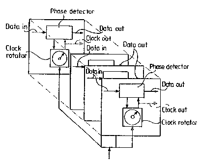
Figure 13 is a schematic perspective view illustrating
use of clock recovery systems according to Figure 1 for clock
CA 02126552 2000-11-20
dV0 93/135U2 PCf/~E92/OU~09
11
recovery in the case of several data flows,
Figure 14 shows a schematic diagram of a circuit for
imparting common phase position to several clock recovered
data flows according to Figure 13,
Figure 15 is a schematic circuit diagram of a further
embodiment of a portion of a ptaase variation circuit included
in the phase correction device,
Figure 1~ is a vector diagram illustrating vari~.tion of
the amplitude of the output clock signal with phase changes
1~ in the circuit according to Figure 15,
Figure 17 is a schematic circuit diagram illustrating a
modification of the circuit according to Figure 15,
Figure 18 is a vector diagram illustrating variation of
the amplitude of the output clock signal with phase changes
in the circuit according to Figure 17,
Figure 19 illustrates a phase variation circuit similar
to the one of Figure 15 but differing therefrom by being
digitally controlled,
Figures 20 and 21 show two embodiments of control logic
circuits for controlling the circuit of Figure 19.
#~referred embodiments.
The system schematically shown in Figure 1 for clock
recovery of a digital data signal Din includes a phase
~5 detector 2. The phase detector 2 has an input 4 for receiving
the data signal Din and an output ~ for emitting the same
after clock recovery. A phase correction system 8 has an
input 7Lt~ for receiving a reference clock signal Ckira, either
from a clock 12 or in the form of an external clock signal.
~teferring also to Figure 2 the phase correction system 8
includes a circuit 14 deriving from the reference clock
sigfnal CKin a number of mutually phase shifted auxiliary
clock signals. The phase correction system 8 is furthermore '
arranged 9~or creating and emitting, in a gray to be described
snore closely' below, a recovered clock signal CKut fox the
data signal. The recovered clock signal is fed to the phase
detector 2 which, in a ~aay to be likewise described more
closely below, detects a phase position error, if any,
between the data signal and its recovered clock signal, and
N~ 93/13602 fCT/SE92/00809
12
emits information with regard to this to the phase correction
system 8. _
The phase correction system 8 includes a phase variation
circuit 16 which, if the phase position error is different
from zero and the phase position of the recovered clock
signal as situated between the phase positions of two of the
auxiliary clock signals, mixes these two auxiliary clock
signals with each other for forming an adjusted recovered
clock signal with the same phase position as the data signal.
This will likewise be described more closely below.
The phase variation circuit Z6 is also referred to as a
clock or phase rotator below.
More particularly, the recovered clock signal CKut is fed
to an input 18 of the phase detector 2 which creates the
phase position information in the form of a current signal
xint2, which is fed to a control input 20 of the circuit 16.
As likewise described more closely below, this current signal
is created so that its amplitude will form a measure of the
magnitude of the phase position error and so that the sign
thereof indicates the direction for adjusting the phase
position of the recovered clock signal.
The design and function of the circuit 14 will now be
described more closely with reference to Figures 2 and 3.
The circuit l4 includes two phase delay and differential
steps 22 and 24, consisting of differential amplifiers, the
speed and band width of which may be controlled by means of
an external .reference current generated in a way described
below.
The delay step 22 on an input 26 receives the clock
signal CKin and delays it with 90°, and emits this 90°
signal
and its antiphase signal, i.e. a~signal phase shifted 270°
with respect to the incoming clock signal CKin, on a
respective output. The 90° phase delayed signal is fed to an
input 28 of tRae delay step 24 which in turn shifts the phase
thereof further by 90°, i.e. to 180° with respect to the
incoming clock signal, and emits this signal and its 360°
antiphase signal on a respective output.
zn Fa.gure 2 aa~d further below the four thus obtained
phase delayed sa.gna~s are indicated with their respective
~' ,'VVO 93/13602 _ ~ ~ ~ ~ ~ ~ PtT»92/00809
23
phase delay values with respect to the clock signal CKin.
The clock signal CKin and the 360° signal are fed to a
plus and a minus input, respectively, of an integrator 30,
the band width of which is s~ lo~a that the output current nay
be regarded as a direct current. The integrator 30 has an
extra gate input 32 for snaking the integrator active only
when a positive signal is received on this input. The 90°
signal is fed to the gate input 32 of the integratoY. Thereby
the integrator 30 is arranged to generate the above ~aentioned
external reference signal for the delay steps ~:2 and 2.4 and
emits the same on an output 33 which is fed back to
respective control inputs 34 and 36 of the two delay steps 22
and 2~ and thereby by means of said reference signal controls
the latter so that they are set to 90° phase delay.
Figures 3a-d show the clock signal CKin, the 90° signal,
the 360° signal and the output signal gintl of the integrator
30 above each other for three different cases following each
other in the horizontal direction. These are phase shift with
exactly 90°, less than 90° and mare than 90°,
respectively,
of the delay steps. The latter two cases involve, as appears
from a comparison of Figure 3a and Figure 3c, a corresponding
phase shift between the clock signal CKin and the 360°
signal, and gives rise to positive and negativ current pulses
from the integrator 30 with a width corresponding to the
phase shift, as appears from Figure 3d. Figure 3e shows the
mean current Tint. as a function of the phase shift or
angular error ~ over a delay step. The output current of the
integrator is thus zero at 90° phase shift.
The design and operation of the delay steps 22 and 24
designed as differential amplifiers according to the above,
as well as of the integrator 30 should be evident to the
ordinary man of the art and need therefore not be described
snore closely below.
The design and function of the phase varying circuit 16
will npw be described snore closely below with reference to
Figures 2 and 4-9.
The 90°~ 1.80°, X70° and 360° output signals
derived from
the delay steps 22 and 24 are fed to a respect~v~e switching
element 38, ~40~ ~~~ and 44, included in the phase varying
...... .......~....._~.......~~.~,.~.....~...r~..~...x~~...............w......
~~~....~.......... ~ ~ F~ ~ . ..~..:~.~
~.~~.....~.....~.wu~.......".._Y_.........._... . _ .....
wo ~3im~oz ~cris~9zioo~o9
14
circuit 16. The switching elements 38-44 can consist of some
form of controllable impedances, e.g. SET resistances or MOS
transistors. ~'he recovered clock signal CF~,at is obtained, in
a way to be described more closely below, on the outputs of.
the switching elements 38-44, said outputs being connected in
parallel to the input 18 of the phase detector 2.
The central input 20 receiving the above-mentioned
current signal fortes the input of an analog selector circuit
46 which, via outputs 48, 50, 52, 54, controls tYae let
710 through of the respective switching elements 38, 40, 42 and
44, of their respective phase shifted signal.
An embodiment of the selector circuit 46 is shawn~in more
detail in Figure 4. The current signal to the selector
circuit 46 is led, on the one hand, to an input 55 of a logic
control network 56 to be described more closely below, which
contains digital logic, and, on the other hand, to a~n analog
swatch 58 receiving the current signal on an input 60 and,
via an inverting amplifier 62, its inverted value an an input
64. The switch 58 has an output connected to an analog
selector 65 with four outputs 68, 70, 72, and 74 connected to
each one of the respective outputs 48, 50, 52 and 54 of the
selector circua.t 4~, and to each one of four inputs 76, 78,
80 and 82, respectively, of the logic control network 56. The
latter has two outputs connected to a control input 84 of the
analog switch 58 and, respectively, to a control input 85 of
the analog selector 66.
The capacitances designated 88, 90, 92 and 94 in Figure 4
of the ~utputs 48-54 represent parasit capacitances and extra
capacitance, ~ if any.
The design of each of the inputs 76, 78, 80, 82 appears
more closely from Figure 5. ~3etween each input and the
digital logic there are trio comparators ~36 and 98 arranged in
parallel. The camparator ~6 an its -a-input receives a control
voltage derived in a way to be disclosed anore closely below
from tl3e current signal, and on its -input a set first
reference sralue refl, and gives maximum output signal if said
control voltage exceeds this reference ~ralue. The comparator
98 in the same way receives on its -input a central voltage
derived in a way to be disclosed more closely ~aelaw from the
lr .l. Fed 49 t~ ci Iw
VV~ 93/13602 - P~6'/~~92/0~8a9
current signal and on its -t-input a set second reference value
ref2, and gives minimum output signal if this control voltage
is lower than this reference value. By means of the above
described function of the two comparators 96 and 98 a
5 detection is carried thr~ugh with respect to when the outputs
from the selector 66 are fully set to minimum or maximum
value, as will be likewise described more closely below.
~aCh Of the inpilt~ 7~~g2 furtherlllore lnClLlde~ two
schematically indicated holding functions in the form of I4OS
10 transistors 100 and 102 of n and p type, respectively,
connected as shown, which are controlled by signals from the
digital logic for holding the corresponding output of the
selector 66 when it has such a phase position that it shall
keep a fixed level 0 or 1 Figure 7), said levels being
15 defined more closely below.
With reference to Figure f> the input 55 of the logic
control network 5S is connected to the digital logic included
therein via a comparator 104, more particularly its -input.
Comparison with a reference value ref3 on the --input of the
2o comparator is carried through for detecting whether the
current signal Iint2 from the detector 2 has a positive or
negativ sign. This gives a detection of whether the phase of
CKut precedes or lags, and enables the digital logic to
change the phase in the correct direction.
The digital techraics of the logic control network 55
provides for the current signal lint2s in accordance with
that which wall be described more closely below, to be
periodically corsnected to the outputs ~a8, 70, 72 and/or 74 in
accordance with a predetermined scheme by means of the analog
selector 56, and so that it becomes the correct sign by means
of the analog switch 58. The current signal charges the
respective capacitances 8$, 90, 92 or 94, tPae resulting
charging voltage of which being applied 'to the control
electrode of the respective switching elements 38, 40, 42 or
44.
Tae scheme menta.~aned above is illustrated most simply by
means of the diagrams of Figures 7a-d. These diagrams
illustrate the charging voltages ua, ub, uc, ud of the
capacf.tanc~s 8894, the degree signs on the lower horizontal
r, _ 2~~b~~~
W~ 93/13602 Pt.'T/SE92/00809
16
common axis representing the phase shift between C3Cin and
CKut. The levels 0 and 1 in the diagrams mean that the
respective signal is completely disconnected or completely
connected into circuit, respectively, which is obtained by
means of the systems described above with reference to figure
5. The ramps represent charge and discharge of the respective
capacitances 88-94, which enables a continuous control of the
switching elements 38-44 and thereby of the phase o~ the
recovered clack signal CKut. More particularly, this is
attained by such a design of the digital logic that its
function can be described by the state graph shown in.Figure
8.
In the state graph according to Figure 8
the state rings represent the successively varying states
of the switching elements 38, 40, 42 and 44, the degree sign
at 'the respective ring indicating the starting point for the
state according to this ring as seen along the horizontal
axis in Figure 7,
the letters a-d represent the respective diagrams a-d in
Figure 7, 'o~0av and °°=3°° in association
with the letter
indicating the state 0 and 1., respectively, of the respective
voltage ua-ud, °'~°° or "_°° in association
with the letter
indicating a state on the positive and negative edge,
respectively, Of tile respective diagram, and
°°max°° ar eemin°°
in association ~rith the letter indicating the end of a
positive or a negative edge, respectively,
~aint2 and -lint2 represent information as to whether the
sign of Iint2 is ~+ or -, respectively.
Tn the ring at 0° in the state graph b=c=0, d=1 involves
that the lagic of the logic control network 56 via the
holding functians 100 and 102 holds the inputs 78 and 80 on
the fixed level 0, and the input 82 on the fixed level 1.
~tegarding eaaWe , °°a°' involves that the logic controls
the
selector 6~ to keep the output s8 open, and °'+°° means
that
the swa.t'ch 58, by the logic detecting ties sign of lint2 at
the input 55 Figure G), is controlled to keep its input 60
open, i.e. Iint~ a.S let through non--inverted by the selector.
~s a result the switching element 44 is kept completely
open for the X60°4°) signal, and the capacitance 88 is
fV~ 93/13502 PC'I'/~E92/00809
~7
charged by the current from the output 68 so that the
switching eleanent 48 successively opens f~r the 90° signal. A
mixing of the two mentioned signals on the common output frcam
the switching elements is. obtained, and results in the phase
of the resulting signal (CKut) successively increasing from
0° as the amplitude of the 90° signal increases. this
corresponds to ~coving upwardly along the positive edge of the
curve a in Figure 7.
If the current Iint~ stops flowing the logic stops, and
the charging of the capacitance 88 stops. Qn one hand, this
results in the switching element 44 henceforth being kept
open due to the fact that the state on the logic input 82 is
kept fixed, and on the other hand, that the capacitance 88
keeps its attained charge, and its voltage maintains the
attained open state of the switch element 38. CKut has been
brought into phase with I~in.
However, if IintZ continues to flow with a positive sign
a state is attained at last where both of the switching
elements 38 and 44 are completely open, which implies that
the phase of CKut has moved halfway between 0° and 90°, i.e.
45~. 'The logic now vii the respective competitor pair 95, 98
(Figures 4,5) senses that its inputs 76 have exceeded the
reference value refs., and via its input 55 (Figure 6) that
the current signal continuous to have a positive sign. This
state, which: is characterized by the state change arrow
e~'~Iint2 & amax°' pointing clockwise from the upper state
circle in Figure 8, brings rthe.logic to keep the attained
state on the input '76, change over Iint2 to the input 64 of
the switch 58, and to open the output 74 for decharging the
capacitance 74 by the changed current flaw direction, cf.
also "d-°' in the 45° circle of Figure 8. the state defa.ned by
the 45°~-circle of the state graph has now been attained. The
resulting decrease of the amplitude of the 360° signal
results in the phase of the signal (CT~t) mixed by the 360°
and 90° signals being continuously changed (along the
negative edge of d in Figure 7) toward 90° which is attained
when the capacitance 94 is entirely decharged, if the current
Iint2 does not became ~:ero before that, in which case the
phase of CICut stops on a value between 45° and 900.
2~.~~~~~
WO 93/13602 PCT~'5~92/00809
18
The state "+lint2 ~' dxain" defined in association with the
clockwise directed state change arrow between the 45° and 90°
state circles has now been attained and is sensed by the
logic as implying that the inputs 78, 8o and 82 take the same
state. 7C~ the sign of Iint2 furthermore continues to be
positive, the logic is now set to open the input 50 of the
switch 58 and the output 70 of the selector ti6 for lint2 with
positive sign, that charges the capacitance 90, gol~owing the
positive edge of curved b in Figure 7, cf. also "b+at in the
1U 90° circle in Figure 8.
As long as lint2 is different from zero the logic
continuous to continously work through the state graph
according to Figure 8 for continuous change of the phase of
CKut, in the same way as has been described above. The
direction is determined by the sign of lint2, i.e. it is
counter clockwise in the graph at negative lint2, following
the inner state change arrows.
~f ~int2 is small, i.e. if a small phase error appears, a
relatively slow recharge is obtained at the respective ~autput
~8-54, whereby a relatively slow phase change is obtained via
the controllable impedances 38-44. The result becomes,
however, a slow movement aroaand according to Figures 7 and 8,
aid thereby a continous phase change.
A greater current xint2 results in a faster recharge of
the capacitances at.the outputs from the analog selector 6f
and thereby a faster phase change.
The magnitude of the capacitancs 88-94 also affects the
speed such as at increasing magnitude the process becomes
slower.
The above described can also be illustrated by means of
the vector diagram according to Figure 9, where the magnitude
of the arrow umix, which represents the signal resulting from
the mixing of two signals, i.e. CKut, gives the amplitude of
this signal for a certain phase,shift a~ between CKut and
CKin. As can be seen the amplitude has maximum at four
occa83ons, J..e. when the 9~°, 1.8~°, 2~~° and
3~~° s>Lgnals,
respectively, are let through unmixed alone.
The iaaplementation in practice of the logic control
network 56, in order to be able to carry through that
2~.~~~~~
W~ 93/13602 ft°I'>5~92/00809
1~
described above with reference to the state graph, is easily
conceivable by the man of the art and need therefore not be
described more closely here. Sh~rtly there can be the
question of a sequence circuit of a conventional
implementation per se, e.g. built from i.a. BIOS~transistors.
For each one of the inputs 60 and 64, and the outputs 68,
70, 72, ~4, respectively, the switches 58 and 66 can be
equipped with suitably connected transmission gates ~.ncluding
MOS~transistors digitally controlled from the control network
56. The inputs 84 and 86 represented in Figure ~ as each a
single input, would then in practice correspond to two and
four control inputs, respectively. ~.lso here 'the man of the
art understands how to carry this through in practice.
Two embodiments of the design and tine function of the
phase detector circuit ~ will now be described more closely
below with reference to Figures 2 and 10, and 11 and 12,
respectively.
In the embodiment according to Figure 2 the input 4 of
the phase detector circuit 2 is connected on the one hand to
an input of an I~2dD gate 156, on the other hand to the D-input
of a MS-flipflop 158~ i.e. an edge trigged D-flipflop. The
clock input of the ~IS~-flipflop 158 is connected to the input
18 for.the reccwered clock signal CICut and its output to an
inverting input of the F~ND~gate 156, the output of which is
connected to the negative input of an integrator 7.60. The
output of the bIS-flipflop 158 is furthermore connected on the
one hand to an input of a further 1~.ND-gate 162, on the other
hand to the D-input of a further MS--flipflop 164. The clock
input of the 1MS-flipflop 164, which is inverting, is likewise
connected to the input 18 for the recovered clock signal
CKut, and its output to an inverting input of an ~~.ND~gate
7.6~, the output of which is connected 'to the positive input
of the integrator 160. The output of the MS-flipflop 7.64 is
also connected tc~ the output 6 'of the phase detector 2 for
providing the data signal Dut after clock recovery. The
output of the integrator 7.60 is connected to the control
input 20 for the selector circuit 46.
~n Figure l0a~g there are shown for three different
cases, which fell~w upon each other in the horizontal
WO 93/13602 fC,'T/SE92/~~809
direction, diagraans over the incoxaing data signal Din, the
recovered clock signal CRut, the output signal D2 from the
MS-flip9~lop 158, the input signal I+ on the plus input of the
integrator 150, the output data signal Dut, the input signal
5 I- on the minus input of the integrator, and the signal
composed of I+ and I-, which by integration gives rise to the
output current Iint2 frown the integrator 1C0. More
particularly, tine three cases are, while referring to the
recovered clock signal CkCut, a correct clock, an early clock,
10 and a late clock, respectively.
The input data signal Din appears on the input of the
AND-gate 1.56, and is clocked into the flipflop 158 by CKut.
When correct clock appears the clocking in is carried through
e~into the middle of the data eye~~ with the positive clock
15 edge. The data signal D1 thereby becomes shifted half a clock
period, is inverted in the inverting input of the AND-gate
156, and forms together with Din on the other input thereof
t9ae signal + on the output of the AND-gte. ~'he positive edge
of the pulses of 'the signal I+ will thereby coincide with
20 positive edges of Din
Due to the inversion of CKut on the clock input of the
MS-flipflop 164 clocking in of D1 in this flipflop will be
carried through in a way similar to that of Din in the
flipflop 3.5g. Dut will thereby be shifted half a clock period
~5 with respect to D1, i.e. Dut and Din will be situated in the
same way with respect to the positive edges of CKut~ Dut is
inverted in the inverting input of AND--gate 162 and forms
together with D1 on the other input thereof the signal I- on
the output of the AND-gate. The positive edge of the pulses
of the signal I-, which in this case are of the same length
as those of the signal I+, will thereby coincide with the
negative edge of I+, which results in the current Iint2
becomming zero.
Tn the two other cases, i.e. early clock and late clock,
respectively, Din is clocked in too early and too late,
respectively, into the flipflop 158 by CKut. 'his gives rise
to the length change of the pulses of the corresponding
signals ~+, which appears froze Figure lOd, whereas the pulses
I- are maintained unchanged. "the respective signals composed
~~_~~J~~
WO 93/13502 i~CT/SE92/00~09
21
of I-~ and I- therefore obtain the appearances shown in Figure
lOg. The result becomes that the current signal Iint2
integrated thereby will be negative at an early clock, and
positive at a late clock.
As should have appeared from the above only the positive
edges of ~in are detected in the embodiment of the phase
detector ~ shown in Figure 2. Setting of the clock can be
made more optimal if both positi~re and negative edges are
detected. This can be carried through in a simple way by the
alternative embodiment of the phase detector shown in Figure
11. More particularly, the ARID-gates of the earlier
embodiment have there been replaced by exclusive-Olt gates
15f>° and 162°, respectively. The corresponding curve shapes
for the same three cases as according to Figure l0a-g are
shown in Figures 12a-g.
The reference clock signal CKin can be common to a number
of clock recovery circuits according to Figure 1, receiving
each its own data flow, as is schematcially illustrated in
Figure 13. Each of the output data flows will then have its
~0 own recovered clock CICut, but these clocks do not have any
common phase position. The latter can in many cases be
desirable, e.g. if the data flows are to be multiplexed
together. d~ circuit to carry this through for each data flow
is shown in Figure 14.
The circuit according to Figure 14 is implemented as a
FIFO consisting of two portions, vii. one portion for reading
the data signal ~ut and its clock CK~t from the clock
recovery circuit, and one portion b for reading out the data
signal the phase of which has been set to the common phase
positi~n. In Figure 1~ the input data signal corresponding to
Dut is designated tfa and its clock with CKa, which thus
corresponds to CZCI.~t. The common clock, to which the
respective phases are to be set is designated CKb, and the
output data signal with Db. Ckb can be the same as CKut from
35. one of the clock recovery circuits, or a separate clack.
The poxtion a includes a first MS-flipflop 170 connected
as a frequency halver by feed back of the inverting output to
the Dm3nput. ~n ids clock input it receives CKa. The flipflop
mutually inverted output signals having half the frequency of
v 2~.~~~i~2
WO 93/13602 fC.'T/SE92/00809
22
OKa are fed to one input of a respective AND°gate 172 and
174, of which the other respective input receives CKa. This
results in every second clock pulse appearing alternatively
on each one of the outputs of the two AND-gates 172 and 174,
said outputs being connected to the clock input of a
respective MS-flipflop 176 and 178. The D inputs of the MS
flipflops 176 and 178 are connected for reception of Da. This
results in every second data bit being clocked inta each a
corresponding one of these MS flipflops.
l0 Reading out in the portion b is carried through in a
corresponding way. The outputs of the MS flipflops 176 and
178 via aaa input of a respective AND-gate 180 and 182, are
connected to each an input of an OR--gate 184. The output of
the OR-gate 184 is connected, on the one hand to the D input
of a N!S flipflop 186 and, on the other hand, via a delay
element 187 to the D input of a MS flipflop 188. The clock
inputs of the his flipflops 186 and 188 receive the clock
signal CKb, which controls the reading out from every second
of the flipflops 1.76 and 178 to the flipflops 186 and 188 in
24 a way which will appear from the following.
34ore particularly, OKb is also fed to the clock input of
a further flipflop 1.90 which in the same way as the flipflop
170 is connected as a frequency halver and has its non-
inverting output connected to one input of an exclusive-OR
.25 gate 1.92, the output of which as connected to the respective
second inputs of the AND°gates 180 and 182, in the latter
case via an inverter 1J4. To the other input of the gate 7.92
the inverting output of a further P4S flipflop 196 is
connected, which is likewise connected as a freguency halver
30 and the clock input of which via an exclusive-OR gate 1.98 is
connected far receiving the signals on the outputs of the HIS
flipflops 196 and 198.
9.'he reading out to the NS flipflop 188 is carried through
via the delay element 187 so that this flipflop receives
35 somewhat delayed data. If the two flipflops 186 and 188 clock
different data the reading is carried through on an edge and
in this position the i4s flipflop 186 is reclocked. This
results in the reading being moved an. entire clock cycle.
This in turn results in resistibility against phase
2.~2~55~
WO~ 93J13fi62 ~~'/SE92/00809
23
variations between the input and output of at least one clock
cycle minus the delay of the element 187. Db is fed out from
the output of the MS flipflop 186.
The FTFO~circuit according to Figure 14 is as short as
possible, vie. only for two bits. This is a minimum for being
able to deal with a phase shift of at least one clock period
between the portions a and b without losing data. The FIFO
can, of course, be made longer if there is a requirement to
being able to deal with greater phase shifts without losing
l0 information.
In the above described embodiments the number of
auxiliary clock signals has furthermore been indicated to be
four. F~er se, this can be regarded being an optimal number,
but neither here there are any limitations. More generally,
the said number can thus be stated to be at least three.
The mixing portion of block or clock rotator l6~in
Figures 1 and 4 can be replaced by some other suitable form
of mixing step, e.g. one of a bipolar type, i.e, a
differential step with current drain, replacing each one of
2o the switching elements 38-X44.
~ne example of such a circuit is shown schematically in
Figure 1.5. The controllable switching means 38-44 in Figure 2
are here replaced by a number of differentially connected
pairs 200, 202, 204, 206 of first and second controlled
switches, here in the form of transistors.
Said pa~.rs are located between voltage source means
indicated by VIE, and a common differential output having
first and second terminals 208 and 210 for forming the common
output for the signal with the desired phase, i.e. CKut. The
3o first and second controlled switches 200.1, 200.2; 202.1,
202.2; 204.1, 204.2; and 206.1, 206.2; respectively, of each
pair have their respective outputs connected to said first
and second terminals 208, 210, respectively.
The differentially connected pairs 200-206 are
furthermore connected, in a way to be described more closely
below, to said °a~oltage source means VFF via current path
means containing current source means and control means
connected to the control outputs 48~54 for controiiing the
current flow. to the differentia~.ly connected pairs 200~206.
WO 93/13602 P~.'Y'1SF92/00809
24
More particularly said current path means comprise a
respective current path for each of said differentially
connected pairs and said current source means comprise a
respective controllable current source 212, 214, 23S - 218
in each current path. Said control means comprise respective
control inputs of said controllable current sources 212-218
connected to the control outputs 48-~54.
~rlso in a way to be described more in detail below, the
transistors of the differentially connected pairs have their
1.0 control inputs, i.e. base electrodes, connected for receiving
the auxiliary clock signals.
More particularly, the differentially connected pairs are
in turn connected in pairs for receiving two of the auxiliary
clock signals as shown in Figure 15. tdith reference to e.g.
the two pairs 200 and 204, it can be seen that the 0°
auxiliary clock signal is received on the base electrode of
the first transistor 200.1 of the differentially connected
pair 200 and on the base electrode of the second transistor
204.2 of the differentially connected pair 204. The 180°
auxiliary signal is received on the base electrode of the
second transistor 200.2 of tlae pair 200 and on the base
electrode of the first transistor 204.1 of the pair 204.
Similarity the differentially connected pairs 202 and 20~
form a pair for receiving the 90° and 270° auxiliary signals
in the same way.
~n Figure 15 it can be seen that a resistance is
indicated in series with each emitter electrode. This
resistance is a so called emitter degenerating resistance for
obtaining improved lineara.~ation of the transistor output
signal. The input signal to the phase rotator should be
triangular or sinus shaped for obtaining monotonously
identical phase steps.
In the vector da.agram according to Figure 15 the
ynagnitude of the arrow umixo in the same way as in Figure 9,
represents the signal resulting from the mixing of two
signals, i.e. CKut, and gives the amplitude of thiw signal
fox a certain phase shift ~p between CTCut and CKin. ids can be
seen the amplitude has maximum at four occasions, i.e. for
45°, 3.35°, 225° and 315° phase shift.
w
WU 93/d3602 d'C°f/SE92/0~~09
Txae circuit according to Figure 15 can be said to provide
active mixing with separate controllable current sources, in
contrast to the circuit with controllable resistances 38-44
in Figure 2, which provides a passive resistive mixing.
5 Figure 17 is a further example of a circuit providing
active mixing, but with a common fixed current source. The
circuit according to Figure 17 differs from that of Figure 15
only by the realization of its current paths connecting its
differentially connected pairs 200-206 of transistors with
10 the potential level ~IEE.
More particularly said current paths comprise a
respective first current path 220, 222, 224 and 226 for each
of the differentially connected pairs and a second current
path 228 common to all differentially connected pairs. 1.~
15 common f axed current source 230 is located in said second
current path, and each of said first current paths includes a
controllable current source 232, 234, 236 and 23g,
respectively, with respective control inputs for connection
to e.g. the control outputs 4d3-54.
20 zn the vector diagram according to Figure 18 the
magnitude of the arrow umix, in the same way as in Figure ~.6,
represents the signal resulting from the mixing of two
signals, i.e. CICut, and gives the amplitude of th~.s signal
for a certain phase shift ~ between Cdcut and CICin. As can be
25 seen the amplitude is taste constant.
In a further embodiment each of~e.g. two differentially
connected pairs, such as those of Figures 15 and 17, may be
connected for receiving the two auxiliary clock signals
alternately on its first and second control inputs. The way
of operation of the circuits according to Figures 15 and ~.7
is 'the same as that described above with reference to Figures
7 and 8.
Figure 1,5 scheanatically illustrates a digital clock
rotator solution having similarities to the circuit of Figure
15. For easy reference similar reference numerals as in
Figuxe 15 are used in Figure 19 for indicating the same or
similar details.
~s in Figure ~.5 the circuit includes four differentially
connected pairs 200~206 of first and second control switches
~~.~~a5~ .
~crm~~zioo~o~
vv~ 93ii~soz
26
connected, in the same way as in Figure 15, between a common
differential output 210, 208 and a common voltage source
means indicated by VEE.
The controllable current sources 212-218 of Figure 15
have, however, been replaced by each a number of n digitally
controlled current sources 1121...n - 2181a..n~ Most simply
there can &~e only one digital current source for each
differential step, which results in a possible resolution of
45°, As the number of simultaneously controlled current
l.0 sources increases it will be possible to obtain a digital
approximation of the sinus and cosinus functions for
obtaining an adjustment with a smooth step resolution and a
relatively smooth output amplitude. The obtainable resolution
and step size is determined by the number of current sources
and their individual weighting, as well as by a control logic
circuit illustrated ira Figure 20.
fihis control logic circuit has as many outputs as the
number of digitally controlled current sources, i.e. a number
of n for each of the differential s~.eps 200-206. For easy
reference the four sets of outputs of the control lagic
circuit and the four sets of control inputs to the digitally
controlled current sources have each been marked ~i8', 50°,
52° and 54', respectively, to underline the similarity to the
circuit of Figure 16.
The logic of the logic circuit is controlled by a ring
counter 250, to be described more in detail below, which
indicates the phase position to be taken by the clock
rotator. The number of phase positions is determined by the
desired degree of resolution.
The phase detector can be the same as in Figure 2 where
the sign of the current lint2 determines whether the clock is
early or late with respect to the phase position of the data
signal. The phase detector can also be a more simple type
which only states whether the timing is late or early.
Figure 20 i3.lustrates haw the signal :~int2 of the phase
detec~IGor is digitised. yint2 is received on the -input of a
comparator 252, the -input of which receives the reference
value re~3, c.f. Figure 6 and the description above referring
thereto. The output signal of the comparator 252 is received
i~'O 93/Y3602 P~'1S1E92/00809
27
on an input of a first AND-gate 254 and on an inverting ~.ayput
of a second AND-gate 256. The respective other inputs of the
gates 254 and 25E receive an adjustment or discriminator
clock signal DCK, which is thereby gated by the comparator
output signal. A high or low output signal from the
comparator indicates if CKin is early or late, respectively.
The outputs from the gates 254 and 256 are received by the
counter 250. The outputs of the counter 250 are received by a
decoder 258 having the outputs 48°-54°.
For early clocking Iint2 is positive, meaning that the
comparator provides a high output signal. This in turn.
results in up counting pulses to the counter 250 with a
frequency determined by 17CK. The up pulses cause forward
counting of the ring counter. This results in the digital
phase rotator increasing the phase until the output signal
Iint2 of the phase detector changes sign. when this happens
the comparator 252 will give a low output signal resulting in
the counter 250 receiving down pulses counting down the
counter until the phase detector again provides a positive
24 output signal, followed by up pulses, etc. In this way the
phase rotator will work to and fro around the desired value.
The phase variation or phase fitter amplitude obtained is
determined by the resolution or step sire of the clock
rotator.
. The speed of the adjustment of the clock phase is
determined by the speed~of DCK and the length of the ring
counter 250. The number of positions for each turn of the
decodes and clock rotator determines the resolution.
The ring counter 250 is an up/down ring counter having no
limitation with respect to the counting seguence up or down.
It works cyclically and when all steps have been passed it
counts further for a new turn. The ring counter running a
turn means that also the clock rotator runs a turn. The
number of steps of the counter.250 is the same as, or more
than the number of states which can be taken by the decoder
258. ~f there are an~re steps in the counter 250 there is
required a number of up or down pulses in sequence for
instructing the de~oeler 250 and the phase rotating circuit to
take a new phase position.
~~~~~52
~c-~~os~9z~oo~o9
WO 93/13602
28
In this manner the output signal of the phase detector
is integrated or filtered. By this error readings, if any, of
the phase detector are suppressed, which can occur due to
fitter in the input signal of the phase rotator.
The frequency of iSCK determines hose often the up or down
pulses can appear, and lianits the maximum speed of rotation
of the phase rotator, this providing a stabilising influence
on the logic in the control loop. DCK can be external or
internally divided down from CKin, which results in a good
control of the different regulation parameters.
It is also conceivable to use a simplified type of .phase
rotator with only two differential steps, which principally
performs the control within only one quadrant at a time (as
opposed to the cases illustrated by Figures W, 1.6 and 1~).
Change of quadrant is possible to obtain by inverting the
input clock signal for change-over to the next quadrant. This
change-over should be carried through, when the next
differential step is still turned off. Thereby a smooth and
continous chanfe-over between the quadrants is obtained.
by such an embodianent it is possible to save logic in the
decoder since it need only control two sets of current
sources (instead of four) plus two clock inverters (for ~ and
90°, respectively).
' Figure 21 illustrates a modification by means of which
also the magnitude of a phase position can be measured. I-n
this embodiment Iint2 is received on the +input of a first
comparator 260 and on the ~-input of a second comparator 262.
Dn their other inputs the comparators 260 and 262 receive a
respective reference signal ref4 and refs. The outputs of the
comparators 260 and 262 are respectively received by an input
of the F~TD-gate 254 and an input of the At~D-gate 256.
If Iint2 is small, resulting in neither up pulses, nor
down pulses, the clock rotator is made to take a stop state
in case of a small phase error. Ian this way a snore quiet
control is obtained although at the cost of a certain
backlash.
plthaugh in the embodiment according to Figure ~.9 the
differential stages are shown and described as co~npr~.si.ng
each a single differentially connected pair of control
WO 93/13602 PC.°I'fS~9x/00809
29
switches and a number of digitally controlled current
sources, it would also be conceivable to let each
differential step comprise several pairs of control stanches
in parallel, e.g. one for each digitally controlled current
source.
It would also be conceivable to use a combination of
digital and. analog control where the digital control is used
for coarse contral and the analog one for fine control.
The invention is furthermore not limited to clock
recovery for a digital data signal, but in its most general
forzu teaches a method for generally shafting the phase.of a
clock signal. This can be conceived if it is imagined that
details 2~6 and 20 are removed from Figures 1 and 2, and
instead a control signal with variable amplitude and sign is
directly fed to the input 20 of the phase varying circuit 16
from e.g, a variable current source. It is also possible to
influence the control logac directly. Tn the digital case in
Figure 20 it is possible to supply counting pulses directly
to the counter 250, or control the decoder directly, i.e.
2fl supplying state code directly thereto.
As has appeared from the above it should once again be
emphasised that the invention suggests a method for generally
shifting or rotating the phase of a clock signal continuously
an arbitrary nu~aber of turns forwards or backwards without
interruptions or discontinuities in the recovered clock
signal.