Note: Descriptions are shown in the official language in which they were submitted.
2126578
HIGH SPECTRAL PURITY
DIGlTAL WAVEFORM SYNTHESIZER ~ -
BACKGROUND
The present invention relates generally to waveforrn synthesizers, and more ;;
panticularly, to a digital waveform synthesizer that employs a direct digital synthesizer
and digital frequency dividers.
An e~isting variable frequency oscillator (VFO) uses a combination of indirect
S frequency synthesis (phase lock loop frequency synthesizer) to provide frequency
upconversion and multiplication, and a direct digital synthesizer using a triangular
waveforrn to generate very fine frequency steps. The use of the phase lock loop
` synthesizer with very narrow bandwidth lirnits the switching speed performance of the
this design. In addition, the phase lock loop scheme uses prograrnmable feedbackdividers that degrade the noise ~and spurious signal) performance inside the phase lock
loop bandwidth by a factor of 20*10g(N), where N is the divider ratio, over the noise
floor of both the frequency divider and the direct digitial synthesizer. The phase lock
Ioop also adds a noise hump near its loop bandwidth. Finally, the triangular waveform
used in the direct digital syn~lesizer generates a higher spur level compared tocornmercially available direct digital synthesizers that generate a sinusoidal waveforrn.
The linear frequency modulated (FM) waveform for use in frequency modulated
ranging (~;MR) is generated by applying a linear voltage rarnp derived from a linear
voltage rarnp generator tO a voltage controUed crystal oscillator (VCXO). The output of
the VCXO is frequency multiplied to X-band to provide rnaximum usable linear FM
¦ 20 biandwidth of 100 KHz. The linearity and the slope accuracy is lirnited by the linearity
of the VCXO and the accuracy of the voltage ramp generator. The slope accuracy is
~` 2 2126~78
increased but at a cost of using multi-unit level calibration and a rnicrowave calibration
target source. Also, the VCXO requires approxirnately 1 KHz of linear frequency
tuning which may be achieved by degrading its FM noise per~orrnance.
Accordingly, it is an objective of the present invention to provide a direct digital
synthesizer that overcomes the limitations of the above~escribed conventional wave-
forrn synthesizers. ln particular, it iS an objec~ve of the present inventic~ to provide a
direct digital synthesizer that provides fast switching, flexible and precisely defined
signals, and that improves the inherently poor spurious signal performance of its direct
digital synthesizer.
SUMMARY OF THE INVENTION
There are many advantages in using a direct digital synthesizer in a frequency
synthesizer, bul a primary disadvantage thereof is that it has inherently high spurious
signal levels. To overcome this problem, the present invention provides for the addi-
~ion of one or multiple frequency dividers in the synthesizer. Onç drawback of this
approach is that the signal bandwidth of the direct digital synthesizer is reduced by the
frequency division factor. However, the present invention is ideally suited for a wave-
fotm generator that requires very high spectral purity but relatively narrow signal
bandwidth.
Thus, in order to meet the above and other objectives, the present invention is a
digital waveforrn synthesizer that comprises a direct digital synthesizer, a waveforrn
generator, a reference frequency generator, and an upconverter and digital frequency
divider circuit. The direct digital synthesizer provides a digitally synthesized input
frequency signal. The digitally synthesized input frequency signal may be a waveform
derived from a waveform generator coupled to the direct digital synthesizer. More
specifically, the wavefortn generator rnay comprise a frequency accumulator adapted to
receive frequency modulated ramp slope signals, and a control and timing circuitcoupled to the frequency accumulator and direct digital synthesizer for synthesizing a
linear frequency modulated waveform.
- 30 A fu st upconverter and divider circuit comprises a mixer having a first input
coupled to the direct digital synthesizer for receiving the synthesized input frequency
signal, and having a second input coupled to the reference signal generator for receiv-
ing a first predetermined reference frequency signal. A bandpass filter is coupled to the
rn~xer, a divide by N divider circuit is coupled to the bandpass filter, where N is the
divide number, and a low pass filter is coupled to the divide by N divider circuit to
complete the first upconverter and divider circuit. The first upconverter and divider
circuit produces a first output signal comprising a first upconverted and divided signal.
~: \
~ 3 2126~78
An output upconverter circuit is coupled to the first upconverter and divider circuit and
comprises a mixer and a bandpass filter. The mixer is coupled to the low pass filter on
one input and has a second input coupled to the reference signal generator for receiving
a second predeterrnined reference frequency signal. The output upconverter circuit
upconverts the first upconverted and divided signal (f~rst OUtput signal) derived from
the digitally synthesized înput frequency signal.
The digital wavefonn synthesizer rnay further comprise additional upconverter
~nd divider circuits coupled between the fiirst upconvener and divider circuit and the
output up~onverter circuit. Each additional upconvener and divider circuits are coupled
to t'ne reference frequency generator for receiving additional predeterrnined frequency
reference signals therefrom.
The digital waveform synthesizer is adapted to generate a linear f~uency
rnodula~ed (FM) waveforrn on a transrnitter drive signal and a receiver first local
oscillator (LO) signal, and a variable frequency oscillator (VFO) signal at a receiver ItQ
reference frequency or at a LO frequency. The frequency divider is used to improve the
inherently poor spurious signal performance of the direct digital synthesizer. The direct
digital synthesizer provides fast switching, flexible and precisely defined frequency
output signals. The digital waveform synthesizer may also be used with any signal
generator that requires high spectral purity and frequency precision, but requires
relatively narrow signal bandwidth.
The digital waveform synthesizer also provides significant perforrnance
improvements over existing variable frequency oscillator and frequency modulatedramp circuit designs. The digital waveforrn synthesizer also requires less hardware to
implement the VFO and FMR functions. For the variable frequency oscillator
application, the digital waveforrn synthesizer provides substantial improvements in
switching speed, spurious signal level, and frequency modulated (FM) noise levels
over the current design described above in the Background section. For the frequency
modulated rarnp applicadon, the digital waveform synthesizer eliminates FMR linearily
and slope errors of the existing design. In addition, the digital waveforrn synthesizer
provides unlimited and flexible FMR slope generation, and eliminates the need for an
elaborate calibration routine and its associated hardware. Furthermore, the digital
waveform synthesizer eliminates FMR requirements from the low noise voltage
controlled crystal oscillator (VCXO), thereby naking extremely low noise crystaloscillator possible, which helps reduce noise.
Additional advantages of the present digital waveform synthesizer include
generation of calibration signals, stretch waveform, and other modulation types. The
4 2126~78
digital waveform synthesizer may be employed with radar systems and missiles with
improved radar perforrnance and reduction in cost.
Two applica~ions of the present digital waveform synthesizer in a high perfor-
rnance airborne radar are as a variable frequency ossillator (VFO) and as a f~quency
5 modulated ranging (FMR) waveform generator. The variable frequency oscilla~or
(VFO) is used to compensate foq Doppler frequency shift in the returnod radar signals.
Its tuning range is approxirnately +250 KHz to -100 KHz for X-band radar.
BRIEF DESCRIPTION OF THE DRAWINGS
The various features and advantages of the present invention may be rnore
readily understood with reference to the following detailed description taken inconjunction with the accompanying drawings, wherein like reference nurnerals
designate like structural elements, and in which:
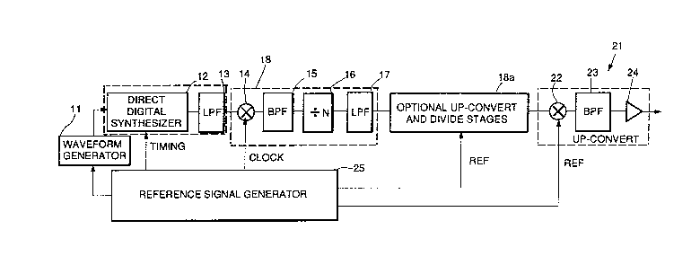
Fig. 1 shows a block diagram of a generic digital waveform synthesizer in
accordance with the principles of the present invention;
Fig. 2 shows a detailed block diagrarn of a digital waveform synthesizer that isused to generate frequency modulated ranging (E;MR) waveform;
Fig. 3 shows a more detailed block diagram of the waveform generator used in
the direct digital synthesizer of Fig. 2; and
Fig. 4 shows a block diagram of a digital waveform synthesizer comprising a
variable frequency oscillator and calibration signal generator.
DETAILED DESCRIPTION
Referring to the drawing figures, Fig. 1. illustrates a generic digital waveformsynthesizer 10 in accordance with the principles of the present invention. The digital
waveforrn synthesizer 10 is comprised of a waveform generator 11 whose output iscoupled through a direct digital synthesizer 12 and a low pass filter 13 to a first upcon-
verter and divider circuit 18. The first upconverter and divider circuit 18 is comprised
of a mixer 14 that has one input coupled to the output of the low pass filter 13. The
output of the mixer 14 is coupled by way of a bandpass filter (BPF) 15 through adivide by N dividcr circuit 16 to a second low pass filter 17. Additional optional
upconverter and divider circuits 18a may be serially coupled to the output of the first
upconverter and divider circuit 18 for a particular application. An output upconverter
circuit 21 is coupled to the output of the first or optional upconverter and divider
circuits 18, 18a, as the case may be. The output upconverter circuit 21 is comprised of
a mixer 22, a second bandpass filter 23 and an arnplifier 24. A reference signal genera-
tor 25 has outputs respectively coupled to the wavefolm generator 11, the direct digital
5 2126~78
synthesizer 12, an input of the mixer 14 of each of the upconverter and divider circuits
18, 1 8a that are used, and the output upconverter circuit 21.
The primary element of the digital waveform synthesizer 10 is the direct digitalsynthesizer 12. The function of the direct digital synthesizer 12 is to generate a
precisely defined signal for the digital waveform synthesizer 10. The ma~n paramelers
of the direct digital synthesizer 12 are spurious signal level and its clock frequency.
The spurious signals generated by the direct digital synthesizer 12 are a function of the
number of bits that ar~ used and the lineari~ of D/A converters employed therein. The
clock frequency determines the maximum output frequency of the direct digital synthe-
sizer 12 ~approxirnately 45% of the clock frequency) which in ~um determines themaximum useful operating bandwidth thereof.
The greater the bandwidth of the direct digital synthesizer 12, the higher the
divider ratio that may be used for a given bandwidth requirement for the digital wave-
form synthesizer 10. Therefore, the direct digital synthesizer 12 is designed to operate
over its entire usable operating bandwidth. However, the direct digital synthesizer 12
may be operated at a narrow bandwidth to avoid frequency regions containing large
spurious signals. The divider circuit 16 improves the spurious signal level by at least a
factor of 20*10g(N), where N is the divide ratio. Therefore1 an ideal direct digital
synthesizer 12 has a high clock frequency and low spurious signals.
Since different direct digital synthesizers 12 may operate at different clock
frequencies with different spur levels, a relative measurement of quality of the direct
digital synthesizer 12 may be roughly defined by multiplication of the spur level and the
square of the maximum clock frequency. Using the above factor as a reference, the
best commercially available direct digital synthesizer 12 is capable of -65 to -70 dBc
worst case spurs at a clock frequency of 60 MHz. This is presently provided by aStanford Telecom I ~C7X series synthesizer, such as a model STEL-1277 direct digital
synthesizer. The performance capabilities of the STEL- 1277 direct digital synthesizer
employed in the present digital waveform synthesizer 10 is sufficient to significantly
improve FMR and VFO circuit performance.
The waveforrn generator 11 provides digital comrnands to the direct digital
synthesizer 12. It may provide a linearly changing frequency cornmand as in the case
of an FMR signal, or a simple frequency comrnand to generate a CW signal in the case
of a VFO signal. Other types of commands may include phase and amplitude
modulation signals.
The first upconverter and divider circuit 18 is used to increase the frequency
output of the direct digital synthesizer 12. This is done for several reasons. First,
since the divider circuit 16 lowers the frequency, upconverting the frequency prior to
212~78
the divider circuit 16 keeps the fre~uency output of the divider circuit 16 high. A
higher frequency speeds up settling of transients introduced into the direct digital
synthesizer 12, and most applil~ations require a ~equency higher than is no~rnally
provided by the direct digital synthesizer 12 alone. l'his has an additional advantage
S that, any spurs introduced by the mixer 14 (mixer intermodulation produc~s) are also
lowered by the divider circuit 16. This is not the case if upconversion is done at the
output of the divider circuit 16. The mixer type, frequencies, and drive levels are
chosen so that the n~Llcer interrnodulation product does not dominate the spurious signal
perfortnance.
T~he reference signal generator 25 provides a reference frequency signal for
upconversion of the signal provided by the direct digital synthesizer 12. For rnost
applications, the reference signal may be a single frequency, but multiple frequencies
may be used to increase the effective bandwidth of the digital waveforrn synthesiær 10.
The frequency, or frequencies, generated by the reference signal generator 25 depends
on the application, but should not be high enough that the bandpass filter 15 cannot
reject low order mixer intermodulation products. Also the spurious and FM noise of
the reference frequency signal should be low enough not to degrade the spur and noise
performance. The reference signal generator 25 is also used to generate a cloclc signal
for the direct digital synthesizer 12 and a drning signal for the waveform generator 11.
The bandpass filter 15 is provided to filter out unwanted mixer intermoduladon
products, and further filter out spurs outside the operating bandwidth. Any interrnodu-
lation products or spurs inside the bandwidth are not attenuated. Also the passband of
the bandpass filter 15 may requlre good phase linearity to minimize modulation
distortion.
The divider circuit 16 is used to improve the spurious signal levels. The typical
spurs from the direct digital synthesizer 12 are single sideband spurs. The divider
circuit 16 attenuates these spurs by a factor of [20*1Og(N)+6] dB. The FM spurs (such
as due to mixer interrnodulation products) are attenuated by 20*1og (N) and AM spurs
are theoretically reduced to zero. An added advantage of the divider circuit 16 is that it
also reduces noise by the same factor. With a relatively high divide ratio, FM noise
perforrnance of the digital waveforrn synthesizer 12 is excellent, and it is set by the
noise floor of Ihe divider circuit 16. One by-product of using the divider circuit 16 is
that the bandwidth of the direct digital synthesizer 12 is reduced by the sarne divide
ratio. Therefore, the by providing a large divider ratio for the direct digital synthesizer
12 results in a very narrow operating bandwidth, unless its bandwidth is extended by
means of multiple reference signals and upconverter and divider circuits 1 8a asrnentioned previously.
7 212~78
The optional upconverter and divider circuits 1 8a rnay be added to increase thetotal divide ratio. The output upconverter circuit 21 is us~d to generate the desired
operating frequency range of the direct digital synthesize~ 12.
Fig. 2 shows a detailed block diagram of a digital wavefo~n synthesizer lOa
S that is used to generate linear FM for frequency modulated ranging (E;MR) applications.
This synthesizer lGa is substantially sirnilar to the generic synthesizer 10 described with
reference to Fig. 1, and includes a single optional upconverter and divider circuit 1 8a.
The specifics of each of the digital waveforrn synthesizer lOa are shown in the drawing
figure, including details of the reference signal generator 25 and the waveform
10 generatol 1 la. A rnore detailed diagram of the wavef~rm generator 1 la is provided in
Fig. 3 and will be described below. The waveform generator 1 la includes an interface
circuit 31 that is coupled to an accumulator circuit 32. The interface circuit 31 is
adapted to receive FMR slope comrnands and timing parameter signals from an external
source (not shown), such as a radar data processor, for example. The reference signal
generator 25 receives a frequency reference input signal, in this case 90.00 MHz. The
reference signal ~enerator 25 is comprised of a buffer amplifier 41 coupled through a
step recovery diode (SRD) frequency multiplier 42 to a power splitter (PS) 43. The
power splitter 43 couples the multiplied input signal by way of a bandpass filter 44a to
a divide-by-three divider 45 whose output is coupled to the accumulator logic 32 and to
20 the direct digital synthesiær 12. An output of the power splitter 43 is coupled through
a bandpass filter 44b to a second power splitter 46 that splits the signal and applies it
through a divide- by-two divider 47 to the mixer in the upconverter and divider circuit
18 and by way of another output to the mixer of the second upconverter and divider
circuit 1 8a. Another output of the power splitter 43 is coupled tl~ough a bandpass filter
25 44c to the mixer of the output upconverter circuit 21. The balance of the digital
waveform synthesizer lOa has been described in detail above, and its design and
construction are considered routine and self-explanatory in view of the drawing figure.
Fig. 3 shows a more detailed block diagram of the waveform generator l l a and
direct digital synthesizer 12 used in the digital waveform synthesizer lOa of Fig. 2.
30 The waveform generator l la includes the interface circuit 31 that comprises a timing
and control circuit 31, such as a programmable gate array model PG-64, manufactured
by Xilinx, for e~ample, and the frequency accumulator 32, such as a model CY7C510
accumulator, manufactured by Cypress, for example. FMR slope input signals derived
from the external source are applied to the frequency accumulator 32 while vanous
35 timing and command signals derived from the external source are applied to the timing
and control circuit 31. 1'he direct digital synthesizer 12 of Fig. 3 is an integrated circuit
that incorporates a model STEL-l 175 numerically controlled oscillator (NCO) 33
2~26~78
coupled to a l(}bit digital-~o-analog converter (DAC) 34. Frequency signals and
cont~ol signals are coupled from the waveform generator 11 a to the nurnericallycontrolled oscillator (NCO) 33 in a conventional manner. The intercoMection and
operation of these circuits are generally well understood by .~hose skilled in the art, and
S r~ay '~e constructed using application notes available from the manufacture~s and
general of circuit design principles.
rne operation of the digital waveform synthesizer lOa will now be descri'~ed.
The digital waveforrn synthesizer lOa is used to generate a linear frequency modulated
signal for use in the frequency modulated ranging for air'oorne radar applications. The
interfacing circuit 3I receives frequency ramp slope and timing signals from theexternal source, such as the radar data processor, for example. The accumulator circuit
32 is loaded with a desired slope value, and given proper ~iiming commands, it updates
the frequency infor;nation provided to the direct digital syntnesizer 12a. The direct
di~,ital synthesizer 12 is clocked at 60 MHz but the frequency is updated at 1/4 of the
clock rate due to internal li nitations. For a typical FMR waveforrn, the direct digital
synthesizer 12 sweeps linea;ly from 5 MHz to 15 MHz in 10 Msec to provide a
frequency ramp slope of I GHz per second. The total bandwidth frorn the direc~ digital
synthesizer 12 is 10 MHz. The waveform is repeated many times for a typical FMR
wavefonn. The output of the direct digital synthesizer 12 is coupled to the low pass
filter 13 to filter the principle DDS spurious signals. The remaining worst casespurious signal level is approximately -70 dBc. The output of the low pass filter 13 is
coupled to the upconversion and divider circuits 18, 1 8a to improve spurious signal
levels. The theoretical spur improvement is better than -45 dB which brings the spur
level below -110 dBc at the output. At the same time, the output bandwidth is reduced
frorn 10 MHz to 100 KHz. The output upconversion circuit 21 using proper reference
signals from the reference generator 25, converts the final output frequency provided
by the digital waveform synthesizer lOa to a specified level.
A summary of the perforrnance of the digital waveforrn synthesizer lOa shown
in Fig. 2 that provides for FMR signals is shown in Table 1.
Table 1
FMR bandwidth 100 KHz
Spurious less than -115 dBc
FM noise less ~han -149 dBclHz (10 KHz out from carrier)
Phase linearity less than 0.1 %
Fig. 4 shows a block diagram of a dual function digital waveforrn synthesizer
10b comprising a variable frequency (VCO) generator 40 that provides for variable
firequency operation, and a calibration signal generator 50. The digital waveform
~`
9 2126578
synthesizer lOb is substantially sirnilar to the circuit shown in Fig. 2, bul does not
include the waveform generator 11. However, the digital waveforrn syrthesizer lOb
additionally includes a calibration signal generator 50, a sw1tch 51 for switching
between the calibration signal generator 50 and the VCO generator 40. In addition, a
S control circuit 52 is coupled to the direct digital synthesizer 12 the processes comrnands
received from the external source (the radar data processor, for example) to control
operation thereof depending upon which geneMtor 4(), 50 (VFO or calibradon signal) is
used Since the calibration signal and VFO signal are not used simultaneously, a single
direct digital synthesizer 12 is used to generate both signals under control of the control
10 circuit 52. The interconnec~ion and operation of these circuits shown in Fig. 4 are
generally well understood by those skilled in the art, and may be constructed using
applica~ion notes available from the manufacturers and general of circuil design princi-
ples. Consequently, and in view of the previous description, a detailed discussion of
the construction of the digital waveforrn synthesizer lOb of Fig. 4 will not be provided.
The operation of the digital waveforrn synthesizer lOb will now be described.
The digital waveforrn synthesizer lOb is used to generate a finely tunable signal for
VFO applications and calibration signals for a radar receiver phase and amplitude
calibration procedure. In both applications, Ihe digital waveforrn synthesizer lOb
generates a continuous wave (CW) signal commanded by the radar data processor. The
control circuit 32 receives frequency and mode (VFO/Calibration mode) commands
from the radar data processor. The frequency inforrnation is appli~d to the direct dig~tal
synthesizer 12 for desired CW frequency generation, and the mode and frequency
command determines the positions of the various switches. In the VFO mode, the
direct digital synthesizer 12 generates a maximu~n signal range from 8 to 21 MHz.
Two stages of upconversion and division are provided by the two upconverter and
divider circuits 18, 18a to improve spurious signal level by better than ~0 dB to give an
output spur level of less than -105 dBc. In the f;rst upconverter and divider circuit 18,
two reference signals are used to effectively double the DDS bandwidth to 26 MHz.
The total bandwidth is reduced to 300 KHz after the second divide by 8 circuit. For the
calibration modes, the two upconverter and divider circuits 18, 18a are bypassed, and
an optional noise source is added to give noise or CW type signals as a calibration
signal. The spurious signal level for the calibration signal is the sarne as that of the
direct digital synthesizer 12 which is adequate for calibration signal purposes. The
output upconverter circuit 21 brings up the output frequencies to the desired level.
3S A summary of performance of the digital waveforrn synthesizer lOb of Fig. 4 is
shown in Table 2.
. . ,o 2126~78
Table 2
~ Calibra~ion si~nal
Bandwidth ~125/~275 KHz + 1 MHz
Spurious less than -105 dBc less than -65 dBc
S FM noise less than -149 dBc/Hz less than -105 dBc/KHz
(10 KHz out l~rom carrier) (10 KHz out from canier~
Switching speed less than 1 ~c less than 1 ~,lsec
Thus there has been described a new and improved digital waveform synthe-
sizer that employs a direct digital synthesizer and digital fiequency dividers. It is to be
10 understood that the above-described embodiment is merely illustrative of some of the
many specific embodiments which represent applications of the pr~nciples of the presen~
invention. Clearly, numerous and other arrangements can be readily devised by those
skilled in the art without departing from the scope of the invention.