Some of the information on this Web page has been provided by external sources. The Government of Canada is not responsible for the accuracy, reliability or currency of the information supplied by external sources. Users wishing to rely upon this information should consult directly with the source of the information. Content provided by external sources is not subject to official languages, privacy and accessibility requirements.
Any discrepancies in the text and image of the Claims and Abstract are due to differing posting times. Text of the Claims and Abstract are posted:
| (12) Patent: | (11) CA 2126610 |
|---|---|
| (54) English Title: | DIGITAL DATA-DEPENDANT AC IMPEDANCE TERMINATION OF TELEPHONE LINE |
| (54) French Title: | IMPEDANCE TERMINALE DE LIGNE TELEPHONIQUE DURANT LA RECEPTION DE DONNEES |
| Status: | Expired and beyond the Period of Reversal |
| (51) International Patent Classification (IPC): |
|
|---|---|
| (72) Inventors : |
|
| (73) Owners : |
|
| (71) Applicants : |
|
| (74) Agent: | OYEN WIGGS GREEN & MUTALA LLP |
| (74) Associate agent: | |
| (45) Issued: | 2003-12-02 |
| (22) Filed Date: | 1994-06-23 |
| (41) Open to Public Inspection: | 1994-12-31 |
| Examination requested: | 2001-03-20 |
| Availability of licence: | N/A |
| Dedicated to the Public: | N/A |
| (25) Language of filing: | English |
| Patent Cooperation Treaty (PCT): | No |
|---|
| (30) Application Priority Data: | ||||||
|---|---|---|---|---|---|---|
|
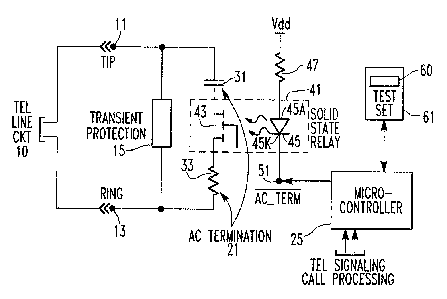
The potential impedance mismatch of digital terminal equipment and a line test
unit conforming with
the Bellcore standard of terminating the line with a 600 - 900 ohm impedance
during data reception includes
a controllably disabled AC impedance, operable to normally bridge the tip and
ring leads of the telephone
circuit under test with the required (600-900 ohm) impedance during data
reception, under direct control by
the craftsman's keypad or software control resident in the test set's
microcontroller, to selectively remove the
AC matching impedance that would otherwise bridge the line. The AC impedance
is comprised of a D.C.
blocking capacitor and a resistor coupled in series with a controllable solid
state relay which is normally
rendered conductive during data reception to bridge the tip and ring leads. By
direct manual control from the
craftsman's keypad, or software control resident in the test set's
microcontroller, the control signal supplied
by the microcontroller to the solid state relay may be removed, so as to
selectively decouple the AC matching
impedance that would otherwise bridge tip and ring leads of the telephone line
during data reception.
Note: Claims are shown in the official language in which they were submitted.
Note: Descriptions are shown in the official language in which they were submitted.
2024-08-01:As part of the Next Generation Patents (NGP) transition, the Canadian Patents Database (CPD) now contains a more detailed Event History, which replicates the Event Log of our new back-office solution.
Please note that "Inactive:" events refers to events no longer in use in our new back-office solution.
For a clearer understanding of the status of the application/patent presented on this page, the site Disclaimer , as well as the definitions for Patent , Event History , Maintenance Fee and Payment History should be consulted.
| Description | Date |
|---|---|
| Time Limit for Reversal Expired | 2007-06-26 |
| Letter Sent | 2006-06-23 |
| Inactive: IPC from MCD | 2006-03-11 |
| Inactive: IPC from MCD | 2006-03-11 |
| Revocation of Agent Requirements Determined Compliant | 2005-01-07 |
| Inactive: Office letter | 2005-01-07 |
| Inactive: Office letter | 2005-01-07 |
| Appointment of Agent Requirements Determined Compliant | 2005-01-07 |
| Letter Sent | 2004-12-14 |
| Letter Sent | 2004-12-14 |
| Revocation of Agent Request | 2004-11-17 |
| Appointment of Agent Request | 2004-11-17 |
| Grant by Issuance | 2003-12-02 |
| Inactive: Cover page published | 2003-12-01 |
| Pre-grant | 2003-08-25 |
| Inactive: Final fee received | 2003-08-25 |
| Notice of Allowance is Issued | 2003-07-28 |
| Letter Sent | 2003-07-28 |
| Notice of Allowance is Issued | 2003-07-28 |
| Inactive: Approved for allowance (AFA) | 2003-07-11 |
| Amendment Received - Voluntary Amendment | 2003-06-05 |
| Amendment Received - Voluntary Amendment | 2003-05-27 |
| Inactive: S.30(2) Rules - Examiner requisition | 2003-03-31 |
| Inactive: Status info is complete as of Log entry date | 2001-04-26 |
| Letter Sent | 2001-04-26 |
| Inactive: Application prosecuted on TS as of Log entry date | 2001-04-26 |
| All Requirements for Examination Determined Compliant | 2001-03-20 |
| Request for Examination Requirements Determined Compliant | 2001-03-20 |
| Application Published (Open to Public Inspection) | 1994-12-31 |
There is no abandonment history.
The last payment was received on 2003-05-12
Note : If the full payment has not been received on or before the date indicated, a further fee may be required which may be one of the following
Patent fees are adjusted on the 1st of January every year. The amounts above are the current amounts if received by December 31 of the current year.
Please refer to the CIPO
Patent Fees
web page to see all current fee amounts.
| Fee Type | Anniversary Year | Due Date | Paid Date |
|---|---|---|---|
| MF (application, 3rd anniv.) - standard | 03 | 1997-06-23 | 1997-06-03 |
| MF (application, 4th anniv.) - standard | 04 | 1998-06-23 | 1998-05-27 |
| MF (application, 5th anniv.) - standard | 05 | 1999-06-23 | 1999-05-05 |
| MF (application, 6th anniv.) - standard | 06 | 2000-06-23 | 2000-04-04 |
| Request for examination - standard | 2001-03-20 | ||
| MF (application, 7th anniv.) - standard | 07 | 2001-06-25 | 2001-05-23 |
| MF (application, 8th anniv.) - standard | 08 | 2002-06-24 | 2002-05-23 |
| MF (application, 9th anniv.) - standard | 09 | 2003-06-23 | 2003-05-12 |
| Final fee - standard | 2003-08-25 | ||
| MF (patent, 10th anniv.) - standard | 2004-06-23 | 2004-05-17 | |
| Registration of a document | 2004-11-15 | ||
| MF (patent, 11th anniv.) - standard | 2005-06-23 | 2005-06-03 |
Note: Records showing the ownership history in alphabetical order.
| Current Owners on Record |
|---|
| FLUKE CORPORATION |
| Past Owners on Record |
|---|
| GEOFFREY H., JR. PARKER |
| MICHAEL D. HORTON |

