Note: Descriptions are shown in the official language in which they were submitted.
METHOD AND APPARATUS FOR CONFIGURING MEhlORY CIRCUITS
2126~21
BA~KGROUND OF THE INVENTION
1. Field of the Invention
This invention relates to configurable electronic
storage devices, particularly to memory cells configured for
emulating circuits including digital memory.
2. Description of the Background Art
In the area of electronic design automation (EDA),
various software and associated hardware are used to define
and verify circuit designs. Particularly to achieve more
accurate verification of circuit designs, EDA tools, known as
"emulators," are employed to construct functional
-epresentations of proto~ype circuit definitions. Because
such emlllated representations allow a circuit designer
flexibly to operate or develop a target system coupled to ~he
emulated representation, even before the prototype circuit or
hardware is actually manufactured, overall design time and
cost is reduced significantly.
Although conventional emulation tools are suited for
defining and verifying logic circuits, such tools are not used
easily for emulating memory circuits, particularly multi-
ported memory circuits configured in various storage
; configurations. It would be desirable, therefore, to provide
memory circuits which are more easily configurable to emulate
prototype circuit designs.
~- .
2126~21
SU~qARY OF T~lE INV~NTION
The invention resides in implementing a memory
circuit definition in at least one of various memory circuits
having multiple access ports, wherein each access port of each
memory circuit, in which the memory circuit definition is
implemented, is configured for either reading from or writing
to each such memory circuit.
Preferably, each memory circuit comprises static
memory cells having three bidirectional access ports, and the
memory circuit definition defines initial storage contents,
depth, width, and bank selection in the memory circuits
according to predefined configuration values. Also the memory
circuit definition may define, for each access port of memory
circuits having the implemented memory circuit definition,
whether such access port is confi~ured for reading or writing.
Optionally, the configured access ports may be
accessed during predefined time slots to read from or write to
the memory circuits. Separate time slots may be predefined
for reading from or writing to the memory circuits, as opposed
to non-memory logic circuits. Time slots may be predefined as
a function of external clock signals and memory circuit access
times.
--2--
: '
:' ',,
- 2126~21
:
Optionally, a prototype circuit definition may be
partitioned into a logic circuit definition for implementation
in a reconfigurable logic module and into the memory circuit
5 definition for implementation in at least one of the memory
circuits. The reconfigurable logic module may be
interconnected directly, or through a programmable
interconnect module, to the memory circuits.
To emulate the partitioned prototype circuit
definition, the reconfigurable logic module and the memory
circuits are interconnected and coupled to a target system,
which is then operated after so coupled. During emulation,
the target system may access the access ports to read from or
15 write to the memory circuits. The target system may also
cause a different memory circuit definition to be implemented
in the memory circuits, whereupon the access ports would be
reconfigured accordingly.
~IEF DESCRIPTION OF THE_DRAWINGS 212 6 ~ 21
FIG. 1 is a block diagram of an electronic design
: automation (EDA) system showing user station 10, debug unit
12, and logic modules 14 coupled to interconnect and memory
modules 20, 100 and to target system 18 through interface pods
16.
FIG. 2 is a block diagram of memory module 100
showing memory array 200 and related circuitry.
FIG. 3 is a block diagram of memory array 200 showing
memory circuit 208 including cells 204 and latches 202.
FIG. 4 is a flow chart showing generally a method
embodying the present invention.
,. ~,.. ~ . .
, , :.: . :
2126621
ESCRIPTION OF THE PREFERRED EMBODIMENTS
FIG. 1 is a block diagram of an electronic design
automation (EDA) system showing engineering workstation or
s user station 10 coupled to debugger or debug unit 12, logic
block modules (LBM) 14, programmable interconnect module (PIM)
20, configurable memory module 100, interface pods 16, and
target system 18. The EDA system, which is configured for
emulation similarly to the "MARS" logic emulation systems
designed by PiE Design Systems, Inc. (Sunnyvale, CA), is used
by a circuit or system designer to define and verify circuit
or system functionality using bread-boarding or emulation
techniques. Additional LBMs 14(N) are used to emulate more
complex circuits or systems.
User station 10 includes a conventional processor
which may couple to a network of similar processors for
communication or distributed processing. User station 10
contains computer-aided engineering and design (CAE/CAD)
software EDA tools for deining and verifying prototype
circuit designs. For example, a circuit designer may use such
tools to enter circuit schematics or synthesize logic gates to
define or design circuit or system functionality or
representation, and then use such tools to simulate or verify
the defined functionality.
: ., : ,
: . . .
-, . ~ . - :
~~ 2126~;Ç~l
The circult designer may perform additional
verification by emulating the defined functionality.
Emulation enables the circuit designer actually to operate an
emulated representation of the prototype circuit in target
system 18, in which the prototype circuit is intended to
operate.
Initially, before a prototype circuit may be
emulated, the circuit designer causes the EDA tools to define,
and preferably verify, a particular circuit design. Once the
circuit design is defined or verified, the circuit designer
causes the ED~ tools to generate a conventional circuit file,
or netlist, which provides a textual listing (i . e ., in ~'ASCII"
format) of components and interconnections within the circuit
design. In accordance with the present invention, each
circuit design is defined to include at least one memory
component as well as logic components.
Debug unit 12, which is coupled to user station 10,
allows the circuit designer to transfer or down-load the
generated netlist from user station 10 to logic modules 14,
incerconnect module 20, and memory module 100. Debug unit 12
also serves as a functional tester and logic analyzer for
verifying the operation of the emulated representation of the
prototype circuit design. Debug unit 12 may operate in either
functional test (debug) mode or emulation (run) mode.
- : . ,
2126~
After a particular netlist is generated, the circuit
designer may cause the EDA tools to receive the netlist to
cause the circuit design or definition contained therein to be
implemented physically or "down-loaded" into various
reconfigurable logic circuits or field-programmable gate
arrays (FPGAs) included in loglc modules 14, in the case of
logic components, and into memory cells or static random
access memory (SRAM) included in memory module 100, in the
case of memory components.
O
Emulation is achieved by programmably configuring,
according to the netlist, the actual interconnection and
functional implementation of reconfigurable logic circuits
included in logic modules 14, and, as necessary, the actual
IS interconnection of reconfigurable electrical paths in
interconnect module and the actual memory configuration and
contents in memory module 100.
The circuit designer invokes a design-import command
'to cause the EDA tools to check, among other things, whether
all logic and memory components included in the netlist are
available or stored in a predefined library or database of
logic and memory representations, as provided respectively in
logic module 14 and memory module 100. Preferably, if a
particular logic or memory component is not available in the
library, then the EDA tool may generate a particular
configuration of a corresponding generic logic or memory
212~2~
~ mponent. In this way, using the EDA tool to generate or
construct a particular component configuration, the circuit
designer may customize or specify more completely certain
functionality or operational parameters of such particular
S configuration.
After the netlist is imported, the circuit designer
may invoke a partitioner progra~ included in the EDA tools to
determine which components included in the netlist are logic
and memory components. Preferably, components which include
binary or digital information configured or arranged for
temporary or permanent storage in conventional or various
combinatorial, sequential, or state devices are determined to
be memory circuits or components. Examples of memory
components include core memory arrays having single or
multiple ports, cache arrays ~including store, tag and status
arrays,) multi-ported register files, microcode read-only
memory (ROM), on-chip random-access memory (RAM), first-
in/first-out (FIFO), and processor memory (including
instruction and data caches, general purpose registers, and
local and main storage RAM).
Other components included in the netlist, typically
including conventlonal combinatorial, sequential, or state
2s circuits configured or designed for non-storage applications,
are determined to be logic circuits or components. It is
possible, as designated by the design engineer, to employ
~- '` , '' , ,
::: - - . ~,; - :- '
: :' .~ ' - ' `
- : : ~ . ~ . ~ ,
: . . .
.
212662~
onventional logic circuits for storage memory-type design
applications.
After determining which netlist components are logic
components and which are memory components, the partitioner
program partltions the netlist for down-loading or actual
functional implementation of the components and
interconnections to logic modules 14, interconnect module 20
or memory module 100.
Loglc components are down-loaded to logic modules 14
to configure logic circuit portions and associated
interconnections, preferably using conventional techniques for
programming or configuring FPGAs or configurable logic blocks
lS (CL~s) contained therein according to the partitioned netlist.
Memory components are down-loaded to memory module 100 as
descrihed further herein. Optionally, memory components may
be down-loaded to logic modules 14 for equivalent functional
implementation therein.
Interconnections in the netlist may be down-loaded
either to logic module 14, using available configurable
interconnect on each logic module 14 or FPGAs contained
therein, or to interconnect module 20, using programmable
interconnect paths or configurable cross-bar switches
available therein.
21266~1
The entire prototype circuit design or definition is
implemented functionally and physically for emulation when all
or the desired portions or sub-netlists of logic and memory
components and interconnections in the netlist are down-loaded
to logic modules 14, memory module 100 and, optionally,
interconnect module 20. Upon such configuration, the
prototype circuit design implemented in logic modules 14,
interconnect module 20, and memory module 100 may be coupled
through various int~rface pods or signal connections 16 to a
conv~ntional port or signal socket in target system 18 for
actual functional operation or emulation therein.
During emulation, target system 18 operates under
normal or close-to-normal conditions or timing, by applying
thereto appropriate data, control, test, power, ground and
other appropriate signals, vectors or stimuli. In this way,
the circuit designer may debug or test the functionality of
target system 18 or the prototype design temporarily
configured for emulation in logic modules 1~, interconnect
module 20 and memory module 100.
Additionally, the circuit designer may determine that
various reconfiguration or functional variation to the
interconnections or components included in the netlist are
necessary to modify or change the prototype circuit design.
Such modification is achieved by the circuit designer causing
the EDA tools to redefine, and if necessary, reverify, the
-10--
. .
. . :. ,,
... .. . .
ototype circuit design. Virtually unlimited number and
extent of different or similar modifications are possible
; because the functional implementation of logic circuits and
; interconnections in logic modules 14, memory circuits in
memory module 100, and interconnections in memory module 100
are reconfigurable or reprogrammable using the EDA tools.
'
FIG. 2 is a block diagram of memory module 100
showing memory array 200 and related circuitry, including
"JTAG" processor or controller 102, time slot or signal
generator 104, memory configuration decoder 108, external
clock or oscillator 106, multiplexer (MUX) 110, reconfigurable
logic or "beta-alpha~ array 118, and bidirectional switch or
latches 112, 114, 116.
In FIG. 3, memory array 200 is shown with various
interconnected memory circuits 208 including digital storage
circuits or cells 204, data latches or switches 202, and
configurable, bidirectional read/write ports 206. Preferably,
cell 204 includes eight 3-port static random access memory
(RAM), wherein each cell 204 is a 32K X 32 SRAM having 25-ns
access time. The access direction for each port 206 is
configured or programmed as either read mode or write mode for
appropriate access to corresponding cell 204, preferably by
configuring or programming the signal switching direction of
switch 112, latch 114 or latch 116 coupled thereto.
2126621
Controller 102 receives partitioned netlist
information including loglc and memory components, ;~
configuration and initialization state information and
interconection, representing prototype circuit designs, which
are down-loaded by the EDA tools from user station 10 or debug
unit 12. Logic component or associated interconnection,
configuration, or initialization information are down-loaded
to program or configure reconfigurable logic devices or FPGAs
included in logic array 118.
Memory component or associated interconnection,
configuration, or initialization information are down-load to
program or configure reconfigurable logic devices or FPGAs
included in logic array 118, reconfigurable memory cells 204,
reconfigurable read/write I/O ports 206 or reconfigurable
bidirectional latches 202 in memory array 200, or
reconfigurable bidirectional switches or latches 112, 114, 116
in memory module 100.
Controller 102 also receives, stores and applies test :~
or boundary scan vectors or patterns for verifying circuit
functionality throughout memory module 100, preferably in ~:
accordance with the JTAG standard, as defined in IEEE Std.
1149.1: "Standard Test Access Port and Boundary Scan
Architecture." Controller 102 is a conventional
microprocessor coupled to time slot generator 104, MUX 110,
and decoder 108 and receives instructions from a host
-12-
. .
212662~
-ocessor, which may be either user station 10 or debug unit
12.
Controller 102 uses a pre-specified instruction set
provided in local disk or memory storage for processing the
down-loading of partitioned netlist information into
configurable memory circuits in memory array 200, preferably
in accordance with the provided EDA tools.
I0 Additional instructions are specified therein for
configuring memory circuits in memory array 200 according to
memory components provided in the netlist, in particular
according to pre-defined configurations values such as port
206 access direction, digital storage content, storage depth
size, storage width size and storage bank selections.
Decoder 108 is a memory configuration decoder
circuit, embodied preferably as a programmable logic array
(PLA) having 93 inputs, wherein 8 input pins are used for
configuration code, 12 input pins are used for bank and sub-
bank select, 24 input pins are used for read/write port
select, 16 input pins are used for memory cell grouping, 8
input pins are used for memory cell enable, 24 pins are used
for port time slot clock, and one input pin is used for system
clock; and 136 outputs, wherein 32 output pins are used for
write enable, 8 output pins are used for global bus enable,
and 96 output pins are used for latch control.
2~2~2~ ~ ~
Time slot generator 104 generates preferably up to 24
time slots or timed signal pulses for 24 ports. Each time
slot has a 40-ns duration, wherein 10 ns is allocated for
address time and 25 ns is allocated for access tlme. A
S programmable delay line may be applied before each time slot,
and actual delay time depends on address to system clock
delay.
Time slot generator 104 operates preferably under the
control of controller 102 to provide tap output signals for
enabling port read/write select and bank/sub-bank select to
generate proper write signal and port data latch control.
Additionally, time slot generator 104 adds read data delay
time to system cycle time whenever the last or most recently
IS read port is followed by more than 4 ports. Preferably,
150 ns of delay time is thereby added.
Logic array 118, which may be coupled to logic
modules 14, includes reconfigurable logic circuits or FPGAs
coupled to MUX 110 and switch or latch 12, 116, 114. Switch
112, latch 114 and latch 116 are reprogrammable bidirectional
digital switches or latches, such as 74F543, which are each
coupled to access por~s 206 for accessing digital information
for reading or writing to cells 204.
As shown in FIG. 3, MUX 110 is coupled to controller
102, decoder 108, memory array 200 and logic array 118; and
-14-
~;'' :,' ~ ' ':: : . '
: -.
~- . ~ - ,
.~ . . ., ,
~ . . :
21266~1
lock 106 is coupled to time slot generator 104 and decoder
108.
.
Preferably, memory module 100 is configured with
s predefined parameters. Memory depth is configured from 1 to
32,767. Bank width is limited to 32, 64, 128 or 256 bits.
Thus, if a memory design uses 95 bits in width, then 128 bits
are specified. Bank select configuration depend on bank
width. For example, 128-bit bank allows no more than two
lo banks because memory module 100 has a 256~bit width maximum.
Sub-bank select configuration is used for partial
write operation. For example, 4-byte select is configured for
32-bit widths, 8-byte select is configured for 64-bit widths,
8 double byte select is configured for 128-bit widths, and 8
quad-byte select is configured for 256-bit width. Sub-bank
select may be disabled if partial write capability is not
required. Moreover, one to 2~ read ports and one to 16 write
ports are preferably configured. The total number of read and
write ports configured is 24.
:
Therefore, in accordance with the present invention,
a memory circuit definition is implemented in at least one of
various memory circuits 200, 208 having multiple access ports
206, wherein each access port 206 of each memory circuit 200,
208, in which the memory circuit definition is implemented, is
configured for either reading from or writing to each such
-15-
emory circuit 200, 208. 212 6 6 21
Preferably, each memory circuit 200, 208 comprises
static memory cells 204 having three bidirectional access
ports 206, and the memory circuit definition defines initial
storage contents, depth, width, and bank selection in the
memory clrcuits 200, 208 according to predefined configuration
values. Representative configuration values are provided in
the attached Table I. Also the memory circuit definition may
define, for each access port 206 of memory circuits 200, 208
having the implemented memory circuit definition, whether such
access port 206 is configured for read or write mode.
Such configuration definition for memory access is
achieved preferably by programming or configuring each
bidirectional switch 112, latch 114, or latch 116, which is
coupled to each of three access ports 206. In this way, each
port 206 is implemented for write-only access (i.e., inbound
signal direction) or read-only access (i.e., outbound signal
direction). Each access port 206 may also be configured
bidirectionally, for read and write access.
Optionally, the same memory circuit definition may be
implemented in each of the memory circuits 200, 208, such
that, fox example, all access ports 206 for each memory
circuit 200, 208 are configured identically.
-16-
:, '. ~ ' :
.~ ,
., ,
.. .. .
,. .. .
,
Optionally, the configured access ports 206 may be
accessed during predefined time slots provided by time slot
generator 104 to read from or write to memory circuits 200,
208. Separate time slots may be predefined (e.g., prior to or
durlng emulation) for reading from or writing to the memory
circuits 200, 208, as opposed to non-memory logic circuits:
Time slots may be predefined as a function of
external clock signals and memory circuit access times, and
specified accordingly by the circuit designer, for example,
during prototype circuit definition (netlisting) or
verification (emulation). During a common or multiplexed time
slot, a set of configured access ports 206 may be accessed in
parallel; or alternatively, a single memory circuit 200, 208
IS may be accessed serially during each time slot (i.e., one at a
time). Moreover, such accessing may be initiated by an
asynchronous read or read-back trigger event.
Preferably, stored digital information is accessed
from memory array 200 in words of equal to or smaller than a ;
predefined size. Thus, when accessed words are larger than
the predefined size, controller 102 partitions or parses such
larger words into word portions which are each smaller than or
equal to the predefined size. Additionally, each word portion
is accessed preferably during different or subsequent time
slots.
-17-
, ~ . , .: ,, : . .: . . . :,,
: ~, . . ~ . - , ., . j,
Optionally, a prototype circuit definltlon may be
partitio~ed into a logic circuit definition for implementation
in a reconfigurable logic module 14 and into the memory
circuit definition for implementation in at least one of the
memory circuits 200, 208. The reconfigurable logic ~odule 14
may be interconnected directly, or through a programmable
interconnect module 20, to the memory circuits 200, 208.
To emulate the partitioned prototype circuit
definition, the reconfigurable logic module 14 and the memory
circuits 200, 208 are interconnected and coupled to target
system 18, which is then operated after so coupled. During
emulation, the target system 18 may access the access ports
206 to read from or write to the memory circuits 200, 208. In
a redefined configuration, target system 18 may also cause a
different memory circuit definition to be implemented in the
memory circuits 200, 208, whereupon the access ports 206 would
be reconfigured accordingly.
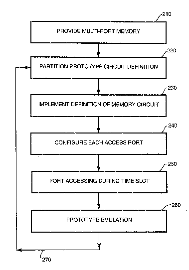
In FIG. 4, a flow chart illustrates generally a
method representative of the present invention. Initially, at
least one memory circuit 100, 200, 208 is provided 210,
wherein each memory circuit includes at least one static
memory cell having preferably three access ports, wherein each
port comprises a bidirectional switch. Then, a prototype
circuit definition, preferably in the form of a netlist, is
partitioned 220 into logic and memory portions.
-18-
- ~ , . - : : ~
2126~21
In accordance with the present invention, the memory
portion or definition is implemented 230 in at least one of
the provided memory circuits, wherein such memory definition
preferably defines intial configuration values. In addition,
each access port 206 of the memory circuits having the
implemented memory definition may be configured 240 for either
reading or writing. Preferably during a predefined time slot,
at least one of the configured access ports is accessed 250 to
lo read or write from such memory circuits.
In the foregoing arrangement, prototype circuit
emulation 260 is thereby enabled, and, as determined
accordingly by the circuit designer, prototype circuit
definition 220 and subsequent steps 230-260 may be repeated
270.
2~26~
TA}3LE I
Configurations for 32-hit data word with 8-bit write select:
CELL: PORT: BANK: SUB-BANK: WRITE: WIDTH: READ WIDTH
8 16W 8R 8 4*8 32 32
S 16W 4R 8 4 32 64
16W 2R 8 4 32 128
16W lR 8 4 32 256
8W 16R 8 4 32 32
8W 8R 8 4 32 64
8W 4R 8 4 32 128
8W 2R 8 4 32 256
8W lR 8 4 32 256
4 8W 4R 4 4 32 32
8W 2R 4 4 32 64
8W lR 4 4 32 128
4W 8R 4 4 32 32
4W 4R 4 4 32 64
4W 2R 4 4 32 128
4W lR 4 4 32 128
2 4W 2R 2 4 32 32 :
4W lR 2 4 32 64
2W 4R 2 4 32 32
2W 2R 2 4 32 64
2W lR 2 4 32 64
1 2W lR 1 4 32 32
lW 2R 1 4 32 32
lW lR 1 4 32 32
--20--
, , ~ . - .
~126~1
Configurations for 64-bit data word with 8-bit write select:
CELL: _QRT: BANK: SUB-BANK: WRITE WIDTH: READ WIDTH
S 8 8W 4R 4 8*8 64 64
8W 2R 4 8 64 128
8W lR 4 8 64 256
4W 8R 4 8 64 64
4W 4W 4 8 64 128
4W 2R 4 8 64 256
4W lR 4 8 64 256
2W 8R 4 8 64 64
2W 4R 4 8 64 128
2W 2R 4 8 64 256
2W lR 4 8 64 256
4 4W 2R 2 8 64 64
4W lR 2 8 64 64
2W 4R 2 8 64 64
2W 2R 2 8 64 128
2W lR 2 8 64 128
2 2W lR 1 8 64 64
lW 2R 1 8 64 64
lW lR 1 8 64 64
2~ 26~1
Configurations for 128-bit data word with 16-bit write select:
5 CELL: PQRT: BANK: SUB-BANK: WRITE WIDTH: READ WIDTH
8 4W 2R 2 8*16 128 128
4W 1~ 2 8 128 128
2W 4R 2 8 128 128
2W 2R 2 8 128 256
2W lR 2 8 128 256
4 2W lR 1 8 128 128
lW 2R 1 8 128 128
lW lR 1 8 128 128
Configurations for 256-bit data word with 32-bit write select:
hh: PORT: BANK: SUB-BANK: WRITE WIDTH: READ WIDTH
8 2W lR 1 8*32 256 256
lW 2R 1 8 256 256
lW lR 1 8 256 256
-22-