Language selection

Search

Patent 2126689 Summary

Third-party information liability

Some of the information on this Web page has been provided by external sources. The Government of Canada is not responsible for the accuracy, reliability or currency of the information supplied by external sources. Users wishing to rely upon this information should consult directly with the source of the information. Content provided by external sources is not subject to official languages, privacy and accessibility requirements.

Claims and Abstract availability

Any discrepancies in the text and image of the Claims and Abstract are due to differing posting times. Text of the Claims and Abstract are posted:

  • At the time the application is open to public inspection;
  • At the time of issue of the patent (grant).
(12) Patent: (11) CA 2126689
(54) English Title: PRINTED CONDUCTIVE INK ELECTROSTATIC SHIELD FOR ELECTROMAGNETIC DIGITIZERS
(54) French Title: BLINDAGE ANTISTATIQUE IMPRIME A L'ENCRE CONDUCTRICE POUR LES NUMERISEURS ELECTROMAGNETIQUES
Status: Deemed expired
Bibliographic Data
(51) International Patent Classification (IPC):
  • H05K 9/00 (2006.01)
  • G06F 3/033 (2006.01)
(72) Inventors :
  • LANDMEIER, WALDO L. (United States of America)
(73) Owners :
  • CALCOMP INC. (United States of America)
(71) Applicants :
(74) Agent: SMART & BIGGAR
(74) Associate agent:
(45) Issued: 1996-09-17
(86) PCT Filing Date: 1992-12-21
(87) Open to Public Inspection: 1993-07-08
Examination requested: 1994-06-23
Availability of licence: N/A
(25) Language of filing: English

Patent Cooperation Treaty (PCT): Yes
(86) PCT Filing Number: PCT/US1992/010994
(87) International Publication Number: WO1993/013509
(85) National Entry: 1994-06-23

(30) Application Priority Data:
Application No. Country/Territory Date
07/816,308 United States of America 1991-12-26

Abstracts

English Abstract


In an electromagnetic digitizer tablet (14) having a grid of receptor wires (30) disposed below a working surface over which
a cursor (12) emanating a magnetic field detected by the receptor wires is moved, this invention is an improvement to reduce elec-
trostatically-caused jitters in data from the receptor wires (30). A grounded electrically conductive shield (40) disposed between
the grid of receptor wires and the working surface (54). The grounded electrically conductive shield (40) is of a material and thick-
ness to pass the magnetic field without substantial attenuation while conducting any electrostatic energy forming thereon to
ground. Both conductive ink and a very thin metal foil can be used for the shield. The digitizer tablet is also shown embodied in
the input/display device of a pen-driven computing system.


Claims

Note: Claims are shown in the official language in which they were submitted.


claims: 8
1. In an electromagnetic digitizer tablet having a grid of
receptor wires disposed below a working surface over which a
cursor emanating a magnetic field detected by the receptor
wires is moved, the improvement to reduce electrostatically-
caused jitters in data from the receptor wires comprising:
a grounded electrically conductive shield disposed
between the grid of receptor wires and the working surface, said
grounded electrically conductive shield being of a material and
thickness to pass the magnetic field without substantial
attenuation while conducting any electrostatic energy forming
thereon to ground.
2. The improvement to all electromagnetic digitizer
tablet of claim 1 wherein:
said grounded electrically conductive shield
comprises a layer of conductive ink disposed between the grid of
receptor wires and the working surface
3. The improvement to an electromagnetic digitizer
tablet of claim 2 wherein:
a) the grid of receptor wires comprises conductive
ink disposed on one side of an insulating substrate; and,
b) said layer of conductive ink comprising said
grounded electrically conductive shield is disposed on an
opposite side of said insulating substrate
4. The improvement to an electromagnetic digitizer
tablet of claim 1 wherein:
said grounded electrically conductive shield
comprises a thin metal foil disposed between the grid of
receptor wires and the working surface.
5. In an electromagnetic digitizer tablet system wherein
a cursor emanating a magnetic field is moved over a working

9
surface of a tablet having a grid of receptor wires disposed
under the working surface and the magnetic field is detected by
the receptor wires, the improved tablet for reducing
electrostatically-caused jitters in data from the receptor wires
comprising:
a) an insulating substrate having the grid of
receptor wires disposed on one side thereof as conductive ink;
and,
b) a grounded electrically conductive shield
disposed on an opposite side of said insulating substrate
between the grid of receptor wires and a working surface of the
tablet, said grounded electrically conductive shield being of a
material and thickness to pass the magnetic field without
substantial attenuation while conducting any electrostatic energy
forming thereon to ground.
6. The improved tablet for an electromagnetic digitizer
tablet of claim 5 wherein:
said grounded electrically conductive shield
comprises a layer of conductive ink disposed on said opposite
side of said insulating substrate.
7. The improved tablet for an electromagnetic digitizer
tablet of claim 5 wherein:
said grounded electrically conductive shield
comprises a thin metal foil disposed on said opposite side of said
insulating substrate.
8. In an electromagnetic digitizer tablet system wherein
a cursor emanating a magnetic field is moved over a working
surface of a tablet having a grid of receptor wires disposed
under the working surface and the magnetic field is detected by
the receptor wires, the improved tablet for reducing


electrostatically-caused jitters in data from the receptor wires
comprising:
a) a flexible insulating substrate having the grid of
receptor wires disposed on one side thereof as conductive ink;
b) an electrically conductive shield disposed on an
opposite side of said flexible insulating substrate as conductive
ink;
c) means for grounding said electrically
conductive shield; and,
d) means for supporting said flexible insulating
substrate whereby the magnetic field is passed through said
electrically conductive shield without substantial attenuation
while any electrostatic energy is conducted to ground by said
electrically conductive shield.
9. In an electromagnetic digitizer tablet system wherein
a cursor emanating a magnetic field is moved over a working
surface of a tablet having a grid of receptor wires disposed
under the working surface and the magnetic field is detected by
the receptor wires, the improved tablet for reducing
electrostatically-caused jitters in data from the receptor wires
comprising:
a) a flexible insulating substrate having the grid of
receptor wires disposed on one side thereof as conductive ink;
b) an electrically conductive shield disposed on an
opposite side of said flexible insulating substrate, said
electrically conductive shield comprising a metal foil thin enough
to pass the magnetic field therethrough without substantial
attenuation while electrically conducting any electrostatic energy
forming thereon;
c) means for grounding said electrically
conductive shield; and,
d) means for supporting said flexible insulating
substrate whereby the magnetic field is passed through said

11

metal foil of said electrically conductive shield without
substantial attenuation while any electrostatic energy is
conducted to ground by said metal foil of said electrically
conductive shield.
10. In an input/display device for a pen-driven
computing system including a liquid crystal display (LCD) panel
with a backlighting panel behind a back surface of the LCD
panel and an electromagnetic digitizer tablet system associated
with the LCD panel wherein a cursor emanating a magnetic
field is moved over a working surface of a tablet disposed
behind the backlighting panel and wherein the tablet has a grid
of receptor wires disposed under the working surface and the
magnetic field is detected by the receptor wires, the improved
tablet for reducing electrostatic interference from the LCD
panel and the backlighting panel with data from the receptor
wires comprising:
a) a flexible insulating substrate having the grid of
receptor wires disposed on one side thereof as conductive ink;
b) an electrically conductive shield disposed on an
opposite side of said flexible insulating substrate as conductive
ink;
c) means for grounding said electrically
conductive shield; and,
d) means for supporting said flexible insulating
substrate behind the backlighting panel whereby the magnetic
field is passed through said electrically conductive shield without
substantial attenuation while any electrostatic energy is
conducted to ground by said electrically conductive shield.
11. In an input/display device for a pen-driven
computing system including a liquid crystal display (LCD) panel
with a backlighting panel behind a back surface of the LCD
panel and an electromagnetic digitizer tablet system associated

12
with the LCD panel wherein a cursor emanating a magnetic
field is moved over a working surface of a tablet disposed
behind the backlighting panel and wherein the tablet has a grid
of receptor wires disposed under the working surface and the
magnetic field is detected by the receptor wires, the improved
tablet for reducing electrostatic interference from the LCD
panel and the backlighting panel with data from the receptor
wires comprising:
a) a flexible insulating substrate having the grid of
receptor wires disposed on one side thereof;
b) an electrically conductive shield disposed on an
opposite side of said flexible insulating substrate;
c) means for grounding said electrically
conductive shield; and,
d) means for supporting said flexible insulating
substrate behind the backlighting panel whereby the magnetic
field is passed through said electrically conductive shield without
substantial attenuation while any electrostatic energy is
conducted to ground by said electrically conductive shield.
12. The improved tablet for an input/display device of a
pen-driven computing system of claim 11 wherein:
said grid of receptor wires and said electrically
conductive shield are composed of a conductive ink.
13. In an input/display device for a pen-driven
computing system including a liquid crystal display (LCD) panel
forming a working surface with a backlighting panel behind a
back surface of the LCD panel and an electromagnetic digitizer
tablet having a grid of receptor wires disposed below the
working surface over which a cursor emanating a magnetic field
detected by the receptor wires is moved, the improvement to
reduce electrostatically-caused jitters in data from the receptor
wires comprising:

13

a grounded electrically conductive shield disposed
between the grid of receptor wires and the working surface, said
grounded electrically conductive shield being of a material and
thickness to pass the magnetic field without substantial
attenuation while conducting any electrostatic energy forming
thereon to ground.
14. The improvement to an input/display device for a
pen-driven computing system of claim 13 wherein:
a) the grid of receptor wires is disposed behind
the backlighting panel; and,
b) said grounded electrically conductive shield is
disposed between the backlighting panel and the grid of
receptor wires.
15. The improvement to an input/display device for a
pen-driven computing system of claim 14 wherein:
said grounded electrically conductive shield is carried
by a back surface of the backlighting panel.

Description

Note: Descriptions are shown in the official language in which they were submitted.


93/13509 ` PCr/US92/10994
212668~

I'RINTIII) CONI)UC1 1V~ INK ELI~CTI~OS1`ATIC
.~1111~.1.1) FOI~ I~Ll~CI'l~O~l~GNl~'lIC DIGITIZE}~S
13~ckPround of the Invention:
This invention relates to digi~izer systems and, more
par~icu]ar~y, in an electromagnetic digitizer tablet having a grid
of receptor wires disposed below a working surface over which a
~ursor emanating a magnetic field detected by the receptor
wires is moved, lo tl~e illll~rovemel~ lo reduce eleclrostalically-
caused jitters in dal~ from tlle receptor wires col~prising a
grounded electrically conductive sl1i~ld disposed between the
grid of receptor wires alld the workiny surface, the grounded
electrically conductive shield being of a ma~erial and t~lickness
to pass tlle magnetic field witllout s~lbsta~ltial attenuation while
conducting any electrostatic energy forming thereon to ground.
20 1~ also relates to digitizers as elllployed as part of the
input/display device of a pen-driven computing system.
In a digitizer system such as that il1dicated as 10 in Figure
1, a cursor 12 connected to a tablet I4 by a connectillg cable ~6
is moved over a wol-king surrace 18 Or the tablet 14 in order to
,'5 input positional dat~ to a colnputer (llot sllown) connected to
the tablet 14. As s~1own il1 tlle cutaway dr~wing Or ~igure 2, tlle
tablet 14 typically coltlprises a plastic upper surface 20 carrying a
grid of electrical conductors 22 wllich interact with a coil 24
within the cursor 12 to provide tl1e positional information
3 0 required. In such systems, it is quite typical to provide a metallic
shield 26 of aluminum, or the like, over the grid of conductors
22. rhe shield 26 acts to magnetically shunt and concentrate
electromagnetic radiatioll from the coil 24 thereby eliminatine
problems of stray fields interacting with undesired wires at the
35 peripheral edges of the grid of conductors 22 in particular.
Where the tablet 14 is moullted in a case 27 as depicted in

WO 93/13!i09 ~,66~ ` PCl'/US92/1~4
~igure 3, the metallic shield 26' may be attached to the bot~on
of the case 27 as with adhesive or the like.
While earlier digitizing systems 10, such as those o~
Figures 1, 2, and 3 employed printed circuit boards with the grid
5 of cQnductors 22 formed thereon either as conductors according
to printed circuit techniques or as actual wires physically
connected to the circuitry of the printed circuit board, more
recently the grid of conductors 22 has been formed on a sheet of
mylar, or the like, employing silk-screening techniques with
o conductive inks. The mylar substrate containing the printed grid
of conductors 22 is then wrapped over and around the edges of
a supporting piece of in~ ting material such as a printed circuit
board, which may or may not contain additional components
and logic associaled with the digitizer system.
When a digitizer tablet constructed according to such
techniques is placed close adjacent a computer terrninal,
electrostatic radiation from the terminal may cause data jitters
in the electromagnetic digitizer. In such construction, the use of
a metal shield 26, as in Figure 2, is not practical and would not
20 solve the particular problem as it is functionally positioned to
shunt a portion of electromagnetic waves and not to pass
electromagnetic waves and shunt electrostatic radiation as is
necessary to solve the problem addressed by the present
invention. l his is particularly true in larger-sized digitizer
25 tablets employed with larger drawings, and the like. A large
~netal shield associated with the tablet is impractical and
unsuitable for solving the problern on the one hand and, even if
it could solve the electrostatic radiation problem, would be cost-
prohibitive on the other hand. Electrostatic interference is also
30 a problem with so-called pen-driven computing systems where a
lligiti7.ing tablet is associated with a back-lit liquid crystal display
panel wherein both the liquid crystal display panel and the
backlighting panel behind it emit electrostatic energy.

_ 3_ 2~2~689
Wherefore lt 18 an ob~ect of the present lnventlon
to provlde a method and apparatus for shleldlng conductlve lnk
flexlble dlgltlzer tablets from the effects of electrostatlc
radlatlon whlle not lnterferlng wlth res~ulred electromagnet~c
f lelds .
It 18 another ob~ect of the present lnvent lon to
provlde a method and apparatus for shleldlng conductlve lnk
flexlble dlgltlzer tablets assoclated wlth back-llt llquld
crystal dlsplay panels ln pen-drlven computlng systems from
the electrostatlc radlatlons of the llquld crystal dlsplay
panel and the back llghtlng panel behlnd lt.
Other ob~ects and beneflts of the lnventlon wlll
become apparent from the detalled descrlptlon whlch follows
herelnafter when taken ln con:lunctlon wlth the drawlng flgures
whlch accompany lt.
6ummary of the Invent lon
The foregoln~ ob~ects have been attalned ln an
electromagnetlc dlgltlzer tablet system whereln a cursor
emanatlng a magnetlc fleld 18 moved over a worklng surface of
a tablet havlng a grld of receptor wlres dlsE~osed under the
worklng surface and the magnetlc fleld 18 detected by the
receptor wlres, by the lmproved tablet of the present
lnventlon for reduclng elect~ostatlcally-caused ~ltters ln
data from the receptor wlres comprlslng a grounded
electrlcally conductlve shleld dlsposed on an opposlte slde of
the lnsulatlng substrate between the grld of receptor wlres
and a worklng surface of the tablet, the grounded electrlcally

72570-3
.. _ . _ .. _ . . ... ....

- 3a - 212~689
conductlve shield being of a material and thickness to pass
the magnetic field without substantial attenuatlon whlle
conductlng any electrostatic energy formlng thereon to ground.
Preferably, the tablet further comprlses an lnsulating
substrate havlng the grid o~ receptor wlres disposed on one
side thereof as conductive ink.


A 72570-3

WO 93/13509 ` PCr/US92/1
~ G~9
In one embodiment, the grounded electrically conductive
shield col~p~i~es a layer of conductive ink disposed on the
opposite side of the insulating substrate.
In another embodiment, the grounded electrically
5 conductive shield comprises a thin metal foil disposed on the
opposite side of the insulating substrate.
In an input/display device for a pen-driven computing
system including a liquid crystal display (LCD) panel forming a
working surface with a b~kli~hting panel behind a back surface
of the LCD panel and an electromagnetic digitizer tablet having
a grid of receptor wires disposed below the working surface over
which a cursor em~n~ting a magnetic field detected by the
receptor wires is moved, the improvement of the present
invention to reduce electr--~t~ti~lly-caused jitters in data from
15 the receptor wires comprises a grounded electrically conductive
shield disposed between the grid of receptor wires and the
working surface, the grounded electrically conductive shield
being of a material and thickness to pass the magnetic field
without su~st~nti~l attenuatioll wllile conducting any
20 electrostatic energy forming thereon to ground.
Preferably in such an implementation, the grid of receptor
wires is disposed behind the backlighting panel and the
grounded electrically conductive shield is disposed between tlle
backlighting panel and the grid of receptor wires. The grounded
25 electrically conductive shield may be carried by a back surface of
the backlighting panel.
lPescription of the Drawings: ~
Figure 1 is a simplified drawing Or a prior art digitizer
30 system comprising a cursor and table~.
Figure 2 is a simplified cutaway drawing througll a typical
prior art digitizer tablet wherein a metal shield is placed over
~he grid of conductors therein to eliminate certain edge ef~ects,

93/13509 PCI/US92/10994
~vo ~12~6~

and the iike, by shunting a portion of the electromagnetic fields
employed in the position-determining process.
Figure 3 is a simplified cutaway drawing througll a typical
prior art digitizer tablet mounted in a plastic case wherein a
5 metal shield such as that of Figure 2 is ~t~h~d to the case.
Figure 4 is a simplifie~ cross-section through a digitizer
tablet according to the present invenlion wherein
electromagnetic fields are passed without attenuation or
shunting and electromagnetic radiation is conducted away to
o ground.
Figure 5 is a simplified cross-section through a digitizer
tablet according to the present invention as employed in
association with a liquid crystal display for use in pen-drive
computing applications.

Description of the Preferred Embodiment:
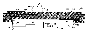
The construction of a digitizing tablet 14' according to the
present invention is shown irl ~igure 4 in simplifled cross-
section. The mylar substrate 28 has the conductive grid ink 30
20 comprising a grid of the tablet 14' applied to a bottom surface
thereof. The mylar substrate 28 is wrapped over and around the
edges of a supporting substrate 32 comprised of a printed circuit
board material, or the like, as sho~ll. The ink 30 of the grid is,
therefore, protected between the supporting substrate 32 and
25 lhe mylar substrate 28. Typically, a thin over-layer 34 of a tough
plastic material is placed over the mylar substrate 28 to protect
it from the continued rubbirlg action of the cursor 12 thereover.
The ink 30 is electrically connected by the wire 36 to the
digitizing logic 38. The digitizing logic 38 may be contained on
30 the printed circuit board CO~ illg the supporting substrate 32,
if desired. To provide the shielding of the present invention, a
printed conductive ink shie!d 40 is applied to the opposite side
of the mylar substrate 28 from the ink 30. The printed
conduc~ive ink shield is further grounded as al 42 and connected

wo 93/13509 6'~'~ 6 PCI/US92/l
as by wire 44 to the digitizing logic 3~. In tested embodiments of
the tablet 14' of Figure 4, it was found that virtually all radiated
electrostatic energy can be eliminated as a sou~ce of noise by
the shielding with no reduction of the electromagnetic field
5 required for accurate sensing. Thus, the conductive ink shield
40 passes the electromagnetic radiation 46 from the cursor 12
through to t~le receiving grid of ink 30 (without shunting it as in
the case of the metal shield 26 of Figure 2) while effectively
conducting away any electrostatic energy 48 to grou~d to
p~revent the undesired jitter noise produced by such electrosta~ic
energy buildup.
While the use of a conductive ink is preferred for the
electrostatic shield 40 because of its ease of application and low
additiona~ cost in a manufacturing process wherein other
15 conductive areas are being applied with conductive inks, other
materials could be employed for tlle shield within the scope and
spirit of the present invention. For example, a grounded thin
metal foil could be applied between the working surface and the
~etecting grid. The only limitation would be that, as opposed to
20 other implementations where a foil is used as a shield such as
the shield 26 of Figure 2 where shunting of electromagne~ic
fields is desired and, thererore, the foil must be greater than a
threshold thickness, if a foil were to be employed to implement
the present invention, it should be less Ihan such threshold
25 thi~kn~cc so that the electromagnetic fields pass therethrough
with virtually no shunting or attenuation. In this regard, the
"foil" could be a very thin layer of metal applied in place such as
with a disposition or similar process as known to those skilled in
the art.
Turning now to Figure 5, the present invention is shown as
incorporated into a pen-driven computing input/display device
50. The pen-driven computing input/display device 50
co.,.p.is~s a case 52 having a liquid crystal display (LCD) panel
S4 at the top thereof. Behind the LCD panel 54 is a

~WO 93/13509 PCI/US92/1~994
~12~68~

backlighting panel 56. Behind the backlighting panel 56 is a
digitizing tablet l 4' according to the present invention
substantially as previously described in detail with respect to
Figure 4. The LCD pane: 54 and b~klightin~ panel 56 are
5 connected by wires 58 to ~pplo~ te display logic 60. lhe
display logic 60 and ~ligiti7in~ logic 38 are connected by a
connecting cable 62 to the pen-driven computer (not shown).
As those skilled in the art will readily recogni~e and appreciate,
if desired the supporting substrate 32 could be eliminated by
~dhesively ~tt~hing the tablet 14' to the back of the
~a~lrlighting panel 56. In such case, the resultant structure of
the pen-driven computing input/display device S0 would be
qui~e thin, as is a primary design goal of such devices. Not being
necessary in this embodiment, the overlayer 34 of the tablet ~4'
15 of Figure 4 is also omitted. Also, in ~uch an embodiment, the
electrostatic shield 40 could, of course, be applied to the back
surface of the backlighting panel 56, if desired, to achieve the
same benefits. The use of an adhesively-back metal foil on the
back surface of the backlighting panel 56 would be particularly
20 applicable in such an embodiment.
Wherefore, having thus described the present invention,
what is claimed is:

Representative Drawing
A single figure which represents the drawing illustrating the invention.
Administrative Status

For a clearer understanding of the status of the application/patent presented on this page, the site Disclaimer , as well as the definitions for Patent , Administrative Status , Maintenance Fee  and Payment History  should be consulted.

Administrative Status

Title Date
Forecasted Issue Date 1996-09-17
(86) PCT Filing Date 1992-12-21
(87) PCT Publication Date 1993-07-08
(85) National Entry 1994-06-23
Examination Requested 1994-06-23
(45) Issued 1996-09-17
Deemed Expired 2000-12-21

Abandonment History

There is no abandonment history.

Payment History

Fee Type Anniversary Year Due Date Amount Paid Paid Date
Application Fee $0.00 1992-12-21
Registration of a document - section 124 $0.00 1994-11-25
Maintenance Fee - Application - New Act 2 1994-12-21 $100.00 1994-12-01
Maintenance Fee - Application - New Act 3 1995-12-21 $100.00 1995-09-27
Maintenance Fee - Patent - New Act 4 1996-12-23 $100.00 1996-09-30
Maintenance Fee - Patent - New Act 5 1997-12-22 $150.00 1997-07-10
Maintenance Fee - Patent - New Act 6 1998-12-21 $150.00 1998-11-03
Owners on Record

Note: Records showing the ownership history in alphabetical order.

Current Owners on Record
CALCOMP INC.
Past Owners on Record
LANDMEIER, WALDO L.
Past Owners that do not appear in the "Owners on Record" listing will appear in other documentation within the application.
Documents

To view selected files, please enter reCAPTCHA code :


To view images, click a link in the Document Description column. To download the documents, select one or more checkboxes in the first column and then click the "Download Selected in PDF format (Zip Archive)" or the "Download Selected as Single PDF" button.

List of published and non-published patent-specific documents on the CPD .

If you have any difficulty accessing content, you can call the Client Service Centre at 1-866-997-1936 or send them an e-mail at CIPO Client Service Centre.


Document
Description 
Date
(yyyy-mm-dd) 
Number of pages   Size of Image (KB) 
Cover Page 1995-07-29 1 22
Cover Page 1996-09-17 1 10
Abstract 1996-09-17 1 38
Description 1996-09-17 8 263
Claims 1996-09-17 6 188
Drawings 1996-09-17 2 66
Abstract 1995-07-29 1 56
Claims 1995-07-29 6 299
Drawings 1995-07-29 2 103
Description 1995-07-29 7 411
Representative Drawing 1998-07-23 1 9
International Preliminary Examination Report 1994-06-23 13 350
Prosecution Correspondence 1996-06-25 1 45
Office Letter 1996-07-19 1 54
Fees 1996-09-30 1 121
Fees 1995-09-27 1 79
Fees 1994-12-01 1 67